View fdms3600as datasheet:

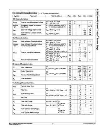
April 2011FDMS3600ASPowerTrench Power StageAsymmetric Dual N-Channel MOSFETFeatures General DescriptionQ1: N-ChannelThis device includes two specialized N-Channel MOSFETs in a dual PQFN package. The switch node has been internally Max rDS(on) = 5.6 m at VGS = 10 V, ID = 15 Aconnected to enable easy placement and routing of synchronous Max rDS(on) = 8.5 m at VGS = 4.5 V, ID = 14 Abuck converters. The control MOSFET (Q1) and synchronousQ2: N-ChannelSyncFET (Q2) have been designed to provide optimal power Max rDS(on) = 1.6 m at VGS = 10 V, ID = 30 Aefficiency. Max rDS(on) = 2.4 m at VGS = 4.5 V, ID = 25 AApplications Low inductance packaging shortens rise/fall times, resulting in lower switching losses Computing MOSFET integration enables optimum layout for lower circuit Communicationsinductance and reduced switch node ringing
Keywords - ALL TRANSISTORS DATASHEET
fdms3600as.pdf Design, MOSFET, Power
fdms3600as.pdf RoHS Compliant, Service, Triacs, Semiconductor
fdms3600as.pdf Database, Innovation, IC, Electricity


LIST
Last Update
BJT: GA1A4M | SBT42 | 2SA200-Y | 2SA200-O | 2SD882-Q | 2SD882-P | 2SD882-E | 2SC945-L | 2SC945-H | 2SC4226-R23 | 2SC3357-F | 2SC3357-E | 2SC3356-R26 | 2SC3356-R24 | 2SC3356-R23 | 2SB772-Q | 2SB772-P | 2SB772-E | 2SA1015-L | 2SA1015-H | HSS8550
Popular searches
irfz44n | irf3205 | irfz44n datasheet | 2n4401 | bc547 transistor | bd139 | 2n4401 datasheet