View ixtk110n20l2 datasheet:
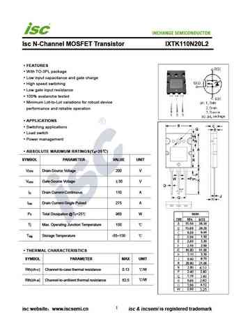
INCHANGE SemiconductorIsc N-Channel MOSFET Transistor IXTK110N20L2FEATURESWith TO-3PL packageLow input capacitance and gate chargeHigh speed switchingLow gate input resistance100% avalanche testedMinimum Lot-to-Lot variations for robust deviceperformance and reliable operationAPPLICATIONSSwitching applicationsLoad switchPower managementABSOLUTE MAXIMUM RATINGS(T =25)aSYMBOL PARAMETER VALUE UNITV Drain-Source Voltage 200 VDSSV Gate-Source Voltage 30 VGSSI Drain Current-Continuous 110 ADI Drain Current-Single Pulsed 275 ADMP Total Dissipation @T =25 960 WD CTj Max. Operating Junction Temperature 150 Storage Temperature -55~150 TstgTHERMAL CHARACTERISTICSSYMBOL PARAMETER MAX UNIT/WRth(ch-c) Channel-to-case thermal resistance 0.13/WRth(ch-a) Channel-to-ambient thermal resi
Keywords - ALL TRANSISTORS DATASHEET
ixtk110n20l2.pdf Design, MOSFET, Power
ixtk110n20l2.pdf RoHS Compliant, Service, Triacs, Semiconductor
ixtk110n20l2.pdf Database, Innovation, IC, Electricity


LIST
Last Update
BJT: GA1A4M | SBT42 | 2SA200-Y | 2SA200-O | 2SD882-Q | 2SD882-P | 2SD882-E | 2SC945-L | 2SC945-H | 2SC4226-R23 | 2SC3357-F | 2SC3357-E | 2SC3356-R26 | 2SC3356-R24 | 2SC3356-R23 | 2SB772-Q | 2SB772-P | 2SB772-E | 2SA1015-L | 2SA1015-H | HSS8550
Popular searches
irfz44n | irf3205 | irfz44n datasheet | 2n4401 | bc547 transistor | bd139 | 2n4401 datasheet