View j111 j112 j113 mmbfj111 mmbfj112 mmbfj113 datasheet:

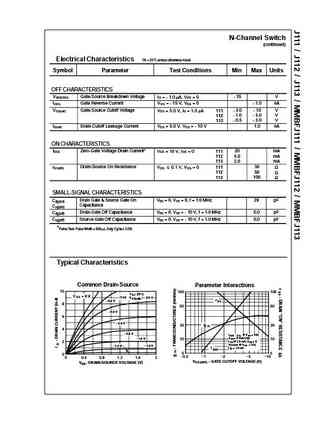
J111 MMBFJ111J112 MMBFJ112J113 MMBFJ113GSG TO-92S SOT-23 DDMark: 6P / 6R / 6SNOTE: Source & Drain are interchangeableN-Channel SwitchThis device is designed for low level analog switching, sampleand hold circuits and chopper stabilized amplifiers. Sourcedfrom Process 51.Absolute Maximum Ratings* TA = 25C unless otherwise notedSymbol Parameter Value UnitsVDG Drain-Gate Voltage 35 VVGS Gate-Source Voltage - 35 V5IGF Forward Gate Current 50 mAOperating and Storage Junction Temperature Range -55 to +150 CTJ ,Tstg *These ratings are limiting values above which the serviceability of any semiconductor device may be impaired.NOTES:1) These ratings are based on a maximum junction temperature of 150 degrees C.2) These are steady state limits. The factory should be consulted on applications involving pulsed or low duty cycle operations.Th
Keywords - ALL TRANSISTORS DATASHEET
j111 j112 j113 mmbfj111 mmbfj112 mmbfj113.pdf Design, MOSFET, Power
j111 j112 j113 mmbfj111 mmbfj112 mmbfj113.pdf RoHS Compliant, Service, Triacs, Semiconductor
j111 j112 j113 mmbfj111 mmbfj112 mmbfj113.pdf Database, Innovation, IC, Electricity


LIST
Last Update
BJT: GA1A4M | SBT42 | 2SA200-Y | 2SA200-O | 2SD882-Q | 2SD882-P | 2SD882-E | 2SC945-L | 2SC945-H | 2SC4226-R23 | 2SC3357-F | 2SC3357-E | 2SC3356-R26 | 2SC3356-R24 | 2SC3356-R23 | 2SB772-Q | 2SB772-P | 2SB772-E | 2SA1015-L | 2SA1015-H | HSS8550
Popular searches
irfz44n | irf3205 | irfz44n datasheet | 2n4401 | bc547 transistor | bd139 | 2n4401 datasheet