View j309g j310g datasheet:
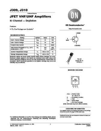
J309, J310Preferred Device JFET VHF/UHF AmplifiersN-Channel DepletionFeatureshttp://onsemi.com Pb-Free Packages are Available*1 DRAINMAXIMUM RATINGSRating Symbol Value Unit3Drain-Source Voltage VDS 25 VdcGATEGate -Source Voltage VGS 25 VdcForward Gate Current IGF 10 mAdc2 SOURCETotal Device Dissipation @ TA = 25C PD 350 mWDerate above = 25C 2.8 mW/CJunction Temperature Range TJ -65 to +125 CStorage Temperature Range Tstg -65 to +150 CMaximum ratings are those values beyond which device damage can occur.Maximum ratings applied to the device are individual stress limit values (notTO-92normal operating conditions) and are not valid simultaneously. If these limits areCASE 29-11exceeded, device functional operation is not implied, damage may occur and1STYLE 5reliability may be affected.23MARKING DIAGRAMJ3xxA
Keywords - ALL TRANSISTORS DATASHEET
j309g j310g.pdf Design, MOSFET, Power
j309g j310g.pdf RoHS Compliant, Service, Triacs, Semiconductor
j309g j310g.pdf Database, Innovation, IC, Electricity


LIST
Last Update
BJT: GA1A4M | SBT42 | 2SA200-Y | 2SA200-O | 2SD882-Q | 2SD882-P | 2SD882-E | 2SC945-L | 2SC945-H | 2SC4226-R23 | 2SC3357-F | 2SC3357-E | 2SC3356-R26 | 2SC3356-R24 | 2SC3356-R23 | 2SB772-Q | 2SB772-P | 2SB772-E | 2SA1015-L | 2SA1015-H | HSS8550
Popular searches
irfz44n | irf3205 | irfz44n datasheet | 2n4401 | bc547 transistor | bd139 | 2n4401 datasheet