View mmbfj111 mmbfj112 mmbfj113 datasheet:
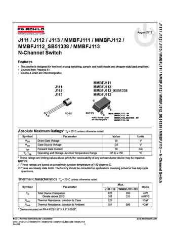
August 2012J111 / J112 / J113 / MMBFJ111 / MMBFJ112 / MMBFJ112_SB51338 / MMBFJ113N-Channel SwitchFeatures This device is designed for low level analog switching, sample and hold circuits and chopper stabilized amplifiers. Sourced from Process 51. Source & Drain are interchangeable.MMBFJ111J111 MMBFJ112J112 MMBFJ112_SB51338J113 MMBFJ113GSSOT-23G TO-92 Mark: MMBFJ111 - 6PSDMMBFJ112 - 6RDNOTE: Source & Drain MMBFJ112_SB51338 - 6Rare interchangeable.MMBFJ113 - 6SAbsolute Maximum Ratings* Ta = 25C unless otherwise noted Symbol Parameter Value UnitsVDG Drain-Gate Voltage 35 VVGS Gate-Source Voltage -35 VIGF Forward Gate Current 50 mATJ, Tstg Operating and Storage Junction Temperature Range -55 to +150 C* These ratings are limiting values above which the serviceability of any semiconductor device may be impaired.NO
Keywords - ALL TRANSISTORS DATASHEET
mmbfj111 mmbfj112 mmbfj113.pdf Design, MOSFET, Power
mmbfj111 mmbfj112 mmbfj113.pdf RoHS Compliant, Service, Triacs, Semiconductor
mmbfj111 mmbfj112 mmbfj113.pdf Database, Innovation, IC, Electricity


LIST
Last Update
BJT: GA1A4M | SBT42 | 2SA200-Y | 2SA200-O | 2SD882-Q | 2SD882-P | 2SD882-E | 2SC945-L | 2SC945-H | 2SC4226-R23 | 2SC3357-F | 2SC3357-E | 2SC3356-R26 | 2SC3356-R24 | 2SC3356-R23 | 2SB772-Q | 2SB772-P | 2SB772-E | 2SA1015-L | 2SA1015-H | HSS8550
Popular searches
irfz44n | irf3205 | irfz44n datasheet | 2n4401 | bc547 transistor | bd139 | 2n4401 datasheet