View pf5103 datasheet:
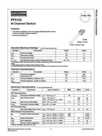
October 2006PF5103tmN-Channel SwitchFeatures This device is designed for low level analog switching sample and hold circuits and chopper stabilized amplifiers. Sourced from process 51. TO-92 Marking : PF51031 2 3 1. Drain 2. Source 3. GateAbsolute Maximum Ratings * Ta = 25C unless otherwise notedSymbol Parameter Value UnitsVDG Drain-Gate Voltage 40 VVGS Gate-Source Voltage -40 VIGF Forward Gate Current 50 mATJ, TSTG Operating and Storage Junction Temperature Range -55 ~ 150 C* These ratings are limiting values above which the serviceability of any semiconductor device may be impaired.NOTES:1) These ratings are based on a maximum junction temperature of 150C.2) These are steady state limits. The factory should be consulted on applications involving pulsed or low duty cycle operations.Thermal Characteristics*Symbol Parameter Val
Keywords - ALL TRANSISTORS DATASHEET
pf5103.pdf Design, MOSFET, Power
pf5103.pdf RoHS Compliant, Service, Triacs, Semiconductor
pf5103.pdf Database, Innovation, IC, Electricity


LIST
Last Update
BJT: GA1A4M | SBT42 | 2SA200-Y | 2SA200-O | 2SD882-Q | 2SD882-P | 2SD882-E | 2SC945-L | 2SC945-H | 2SC4226-R23 | 2SC3357-F | 2SC3357-E | 2SC3356-R26 | 2SC3356-R24 | 2SC3356-R23 | 2SB772-Q | 2SB772-P | 2SB772-E | 2SA1015-L | 2SA1015-H | HSS8550
Popular searches
irfz44n | irf3205 | irfz44n datasheet | 2n4401 | bc547 transistor | bd139 | 2n4401 datasheet