View tw7404fj datasheet:
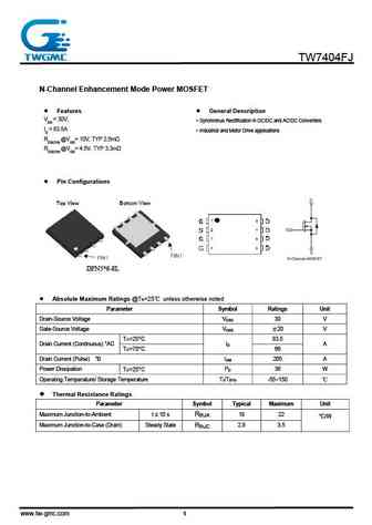
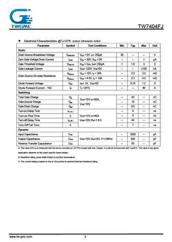
TW7404FJN-Channel Enhancement Mode Power MOSFET Features General Description VDS = 30V, Synchronus Rectification in DC/DC and AC/DC Converters ID = 83.5A Industrial and Motor Drive applications RDS(ON) @VGS= 10V, TYP 2.5m RDS(ON) @VGS= 4.5V, TYP 3.3m Pin Configurations DFN5*6-8L Absolute Maximum Ratings @T =25 unless otherwise noted AParameter Symbol Ratings Unit Drain-Source Voltage VDSS 30 V Gate-Source Voltage VGSS 20 V TC=25C 83.5 Drain Current (Continuous) *AC ID A TC=70 66 C Drain Current (Pulse) *B IDM 205 A Power Dissipation TC=25C PD 36 W Operating Temperature/ Storage Temperature TJ/TSTG -55~150 Thermal Resistance Ratings Parameter Symbol Typical Maximum Unit Maximum Junction-to-Ambient t 10 s R 18 22 thJA C/W Maximum Junction-to-Case (Drain) Steady State R 2.8 3.5
Keywords - ALL TRANSISTORS DATASHEET
tw7404fj.pdf Design, MOSFET, Power
tw7404fj.pdf RoHS Compliant, Service, Triacs, Semiconductor
tw7404fj.pdf Database, Innovation, IC, Electricity


LIST
Last Update
BJT: GA1A4M | SBT42 | 2SA200-Y | 2SA200-O | 2SD882-Q | 2SD882-P | 2SD882-E | 2SC945-L | 2SC945-H | 2SC4226-R23 | 2SC3357-F | 2SC3357-E | 2SC3356-R26 | 2SC3356-R24 | 2SC3356-R23 | 2SB772-Q | 2SB772-P | 2SB772-E | 2SA1015-L | 2SA1015-H | HSS8550
Popular searches
irfz44n | irf3205 | irfz44n datasheet | 2n4401 | bc547 transistor | bd139 | 2n4401 datasheet