ftx30p35g.pdf Principales características:
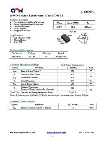
FTX30P35G 350V P-Channel Enhancement Mode MOSFET General Features Proprietary Advanced Planar Technology BVDSS RDS(ON) (Max.) ID Rugged Polysilicon Gate Cell Structure Fast Switching Speed -350V 30 -200mA RoHS Compliant Halogen-free available SOT-89 D Applications Drain High Efficiency SMPS G Gate Adaptor/Charger Drain Active PFC Source S Ordering Information Part Number Package Marking Remark FTX30P35G SOT-89 P35 Halogen Free Absolute Maximum Ratings TA=25 unless otherwise specified Symbol Parameter FTX30P35G Unit VDSS Drain-to-Source Voltage[1] -350 V ID Continuous Drain Current -0.2 A IDM Pulsed Drain Current[2] -0.6 PD Power Dissipation 1.0 W VGS Gate-to-Source Voltage 20 V Soldering Temperature TL 300 Distance of 1.6mm from case for 10 seconds TJ and TSTG Operating and Stor
Keywords - ALL TRANSISTORS. Principales características
ftx30p35g.pdf Design, MOSFET, Power
ftx30p35g.pdf RoHS Compliant, Service, Triacs, Semiconductor
ftx30p35g.pdf Database, Innovation, IC, Electricity
Parámetros del transistor bipolar y su interrelación.
🌐 : EN ES РУ

Liste
Recientemente añadidas las descripciónes de los transistores:
BJT: ZDT6705 | GA1L4Z | GA1A4M | SBT42 | 2SA200-Y | 2SA200-O | 2SD882-Q | 2SD882-P | 2SD882-E | 2SC945-L | 2SC945-H | 2SC4226-R23 | 2SC3357-F | 2SC3357-E | 2SC3356-R26 | 2SC3356-R24 | 2SC3356-R23 | 2SB772-Q | 2SB772-P | 2SB772-E | 2SA1015-L
Popular searches
irfz44n | irf3205 | irfz44n datasheet | 2n4401 | bc547 transistor | bd139 | 2n4401 datasheet