2n5401csm.pdf Principales características:
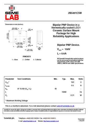
2N5401CSM Dimensions in mm (inches). Bipolar PNP Device in a 0.51 0.10 Hermetically sealed LCC1 (0.02 0.004) 0.31 rad. (0.012) Ceramic Surface Mount 3 Package for High Reliability Applications 21 1.91 0.10 (0.075 0.004) A 0.31 rad. Bipolar PNP Device. (0.012) 3.05 0.13 (0.12 0.005) 1.40 (0.055) 1.02 0.10 max. VCEO = 150V A = (0.04 0.004) IC = 0.6A PINOUTS All Semelab hermetically sealed products 1 Base 2 Emitter 3 - Collector can be processed in accordance with the requirements of BS, CECC and JAN, JANTX, JANTXV and JANS specifications Parameter Test Conditions Min. Typ. Max. Units VCEO* 150 V IC(CONT) 0.6 A hFE @ 10./60 (VCE / IC) 40 - ft 100M Hz PD 0.31 W * Maximum Working Voltage This is a shortform datasheet. For a full datasheet please contact sales@semelab.co.uk. Semelab Plc reserves the
Keywords - ALL TRANSISTORS. Principales características
2n5401csm.pdf Design, MOSFET, Power
2n5401csm.pdf RoHS Compliant, Service, Triacs, Semiconductor
2n5401csm.pdf Database, Innovation, IC, Electricity
Parámetros del transistor bipolar y su interrelación.
🌐 : EN ES РУ

Liste
Recientemente añadidas las descripciónes de los transistores:
BJT: ZDT6705 | GA1L4Z | GA1A4M | SBT42 | 2SA200-Y | 2SA200-O | 2SD882-Q | 2SD882-P | 2SD882-E | 2SC945-L | 2SC945-H | 2SC4226-R23 | 2SC3357-F | 2SC3357-E | 2SC3356-R26 | 2SC3356-R24 | 2SC3356-R23 | 2SB772-Q | 2SB772-P | 2SB772-E | 2SA1015-L
Popular searches
irfz44n | irf3205 | irfz44n datasheet | 2n4401 | bc547 transistor | bd139 | 2n4401 datasheet