2n4393c1a 2n4393c1b 2n4393c1c 2n4393c1d.pdf datasheet:

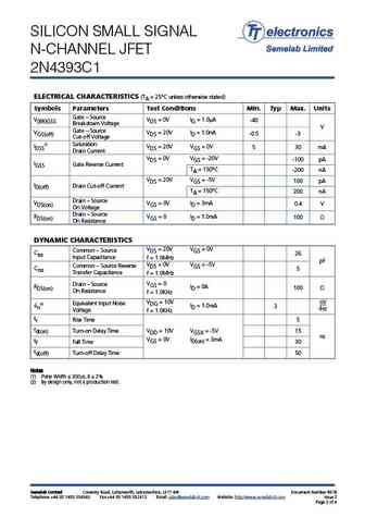
SILICON SMALL SIGNAL N-CHANNEL JFET 2N4393C1 Hermetic Surface Mounted Package. Designed For High Reliability and Space Applications. Screening Options Available. ABSOLUTE MAXIMUM RATINGS (TA = 25C unless otherwise stated) VDS Drain Source Voltage 40V VGS Gate Source Voltage -40V VGD Gate Drain Voltage -40V IG Gate Current 50mA PD TA = 25C Total Power Dissipation at 300mW Derate Above 25C 2mW/C TJ Junction Temperature Range -55 to +175C Tstg Storage Temperature Range -65 to +200C THERMAL PROPERTIES Symbols Parameters Min. Typ. Max. Units RJA Thermal Resistance, Junction To Ambient 500 C/W Semelab Limited reserves the right to change test conditions, parameter limits and package dimensions without notice. Information furnished by Semelab is believed to be both accurate and reliable at the time o
Keywords - ALL TRANSISTORS DATASHEET
2n4393c1a 2n4393c1b 2n4393c1c 2n4393c1d.pdf Design, MOSFET, Power
2n4393c1a 2n4393c1b 2n4393c1c 2n4393c1d.pdf RoHS Compliant, Service, Triacs, Semiconductor
2n4393c1a 2n4393c1b 2n4393c1c 2n4393c1d.pdf Database, Innovation, IC, Electricity


Liste
Recientemente añadidas las descripciónes de los transistores:
BJT: GA1A4M | SBT42 | 2SA200-Y | 2SA200-O | 2SD882-Q | 2SD882-P | 2SD882-E | 2SC945-L | 2SC945-H | 2SC4226-R23 | 2SC3357-F | 2SC3357-E | 2SC3356-R26 | 2SC3356-R24 | 2SC3356-R23 | 2SB772-Q | 2SB772-P | 2SB772-E | 2SA1015-L | 2SA1015-H | HSS8550
Popular searches
irfz44n | irf3205 | irfz44n datasheet | 2n4401 | bc547 transistor | bd139 | 2n4401 datasheet