cem2133.pdf datasheet:
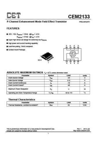
CEM2133P-Channel Enhancement Mode Field Effect Transistor PRELIMINARYFEATURES-20V, -10A, RDS(ON) = 18m @VGS = -4.5V. RDS(ON) = 27m @VGS = -2.5V.Super high dense cell design for extremely low RDS(ON).High power and current handing capability.D D D DLead-free plating ; RoHS compliant.8 7 6 5Surface mount Package.SO-81 2 3 41 S S S GABSOLUTE MAXIMUM RATINGS TA = 25 C unless otherwise notedParameter Symbol Limit UnitsDrain-Source Voltage VDS -20 VGate-Source Voltage VGS 12 VDrain Current-Continuous ID -10 ADrain Current-Pulsed a IDM -40 AMaximum Power Dissipation PD 3 WOperating and Store Temperature Range TJ,Tstg -55 to 175 CThermal CharacteristicsParameter Symbol Limit UnitsThermal Resistance, Junction-to-Ambient b RJA 50 C/WThis is preliminary information on a new product in development now . Rev 1. 2013.JanDetails are s
Keywords - ALL TRANSISTORS DATASHEET
cem2133.pdf Design, MOSFET, Power
cem2133.pdf RoHS Compliant, Service, Triacs, Semiconductor
cem2133.pdf Database, Innovation, IC, Electricity


Liste
Recientemente añadidas las descripciónes de los transistores:
BJT: GA1A4M | SBT42 | 2SA200-Y | 2SA200-O | 2SD882-Q | 2SD882-P | 2SD882-E | 2SC945-L | 2SC945-H | 2SC4226-R23 | 2SC3357-F | 2SC3357-E | 2SC3356-R26 | 2SC3356-R24 | 2SC3356-R23 | 2SB772-Q | 2SB772-P | 2SB772-E | 2SA1015-L | 2SA1015-H | HSS8550
Popular searches
irfz44n | irf3205 | irfz44n datasheet | 2n4401 | bc547 transistor | bd139 | 2n4401 datasheet