j105 j106 j107 jftj105.pdf datasheet:

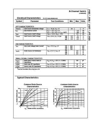
J105 JFTJ105J106J107GDGSSOT-223TO-92GSNOTE: Source & DrainD are interchangeableN-Channel SwitchThis device is designed for analog or digital switching applications wherevery low On Resistance is mandatory. Sourced from Process 59.Absolute Maximum Ratings* TA = 25C unless otherwise notedSymbol Parameter Value UnitsVDG Drain-Gate Voltage 25 VVGS Gate-Source Voltage - 25 VIGF Forward Gate Current 10 mA5Operating and Storage Junction Temperature Range -55 to +150 CTJ, Tstg *These ratings are limiting values above which the serviceability of any semiconductor device may be impaired.NOTES:1) These ratings are based on a maximum junction temperature of 150 degrees C.2) These are steady state limits. The factory should be consulted on applications involving pulsed or low duty cycle operations.Thermal Characteristics TA = 25C unle
Keywords - ALL TRANSISTORS DATASHEET
j105 j106 j107 jftj105.pdf Design, MOSFET, Power
j105 j106 j107 jftj105.pdf RoHS Compliant, Service, Triacs, Semiconductor
j105 j106 j107 jftj105.pdf Database, Innovation, IC, Electricity


Liste
Recientemente añadidas las descripciónes de los transistores:
BJT: GA1A4M | SBT42 | 2SA200-Y | 2SA200-O | 2SD882-Q | 2SD882-P | 2SD882-E | 2SC945-L | 2SC945-H | 2SC4226-R23 | 2SC3357-F | 2SC3357-E | 2SC3356-R26 | 2SC3356-R24 | 2SC3356-R23 | 2SB772-Q | 2SB772-P | 2SB772-E | 2SA1015-L | 2SA1015-H | HSS8550
Popular searches
irfz44n | irf3205 | irfz44n datasheet | 2n4401 | bc547 transistor | bd139 | 2n4401 datasheet