msw20n60.pdf datasheet:

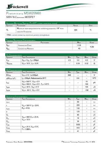
Preliminary MSW20N60 500V N-Channel MOSFET Description This latest technology has been especially designed to minimize on-state resistance, have a high rugged avalanche characteristics. These devices are well suited for high efficiency switch mode power supplies. Features RDS(on) (Typical 0.26 )@VGS=10V Gate Charge (Typical 80nC) Improved dv/dt Capability, High Ruggedness 100% Avalanche Tested Maximum Junction Temperature Range (150C) RoHS compliant package Packing & Order Information 30/Tube ; 540/Box Graphic symbol MAXIMUM RATINGS AND ELECTRICAL CHARACTERISTICS Absolute Maximum Ratings (Tc=25C unless otherwise noted) Symbol Parameter Value Unit VDSS Drain-Source Voltage 600 V 30 VGS Gate-Source Voltage V 20 A Drain Current -Continuous (TC=25C) ID 12 A Drain Current -Continuous (TC=100C) IDM D
Keywords - ALL TRANSISTORS DATASHEET
msw20n60.pdf Design, MOSFET, Power
msw20n60.pdf RoHS Compliant, Service, Triacs, Semiconductor
msw20n60.pdf Database, Innovation, IC, Electricity


Liste
Recientemente añadidas las descripciónes de los transistores:
BJT: GA1A4M | SBT42 | 2SA200-Y | 2SA200-O | 2SD882-Q | 2SD882-P | 2SD882-E | 2SC945-L | 2SC945-H | 2SC4226-R23 | 2SC3357-F | 2SC3357-E | 2SC3356-R26 | 2SC3356-R24 | 2SC3356-R23 | 2SB772-Q | 2SB772-P | 2SB772-E | 2SA1015-L | 2SA1015-H | HSS8550
Popular searches
irfz44n | irf3205 | irfz44n datasheet | 2n4401 | bc547 transistor | bd139 | 2n4401 datasheet