p1503bvg.pdf datasheet:
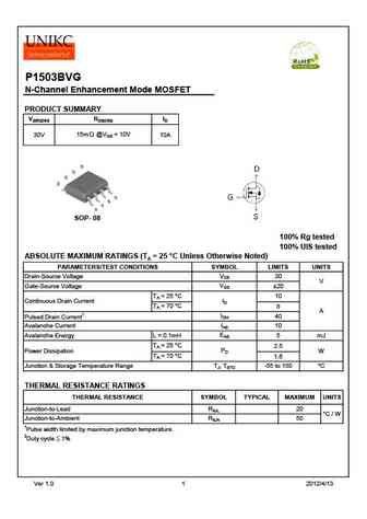
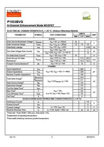
P1503BVGN-Channel Enhancement Mode MOSFETPRODUCT SUMMARYV(BR)DSS RDS(ON) ID30V 15m @VGS = 10V 10ASOP- 08100% Rg tested100% UIS testedABSOLUTE MAXIMUM RATINGS (TA = 25 C Unless Otherwise Noted)PARAMETERS/TEST CONDITIONS SYMBOL LIMITS UNITSVDSDrain-Source Voltage 30VVGSGate-Source Voltage 20TA = 25 C10IDContinuous Drain CurrentTA = 70 C8AIDM40Pulsed Drain Current1IASAvalanche Current 10EASAvalanche Energy L = 0.1mH 5 mJTA = 25 C2.5PDPower Dissipation WTA = 70 C1.6TJ, TSTGJunction & Storage Temperature Range -55 to 150 CTHERMAL RESISTANCE RATINGSTHERMAL RESISTANCE SYMBOL TYPICAL MAXIMUM UNITSJunction-to-Lead RqJL 20C / WJunction-to-Ambient RqJA 501Pulse width limited by maximum junction temperature.2Duty cycle 1%Ver 1.0 1 2012/4/13P1503BVGN-Channel Enhancemen
Keywords - ALL TRANSISTORS DATASHEET
p1503bvg.pdf Design, MOSFET, Power
p1503bvg.pdf RoHS Compliant, Service, Triacs, Semiconductor
p1503bvg.pdf Database, Innovation, IC, Electricity


Liste
Recientemente añadidas las descripciónes de los transistores:
BJT: GA1A4M | SBT42 | 2SA200-Y | 2SA200-O | 2SD882-Q | 2SD882-P | 2SD882-E | 2SC945-L | 2SC945-H | 2SC4226-R23 | 2SC3357-F | 2SC3357-E | 2SC3356-R26 | 2SC3356-R24 | 2SC3356-R23 | 2SB772-Q | 2SB772-P | 2SB772-E | 2SA1015-L | 2SA1015-H | HSS8550
Popular searches
irfz44n | irf3205 | irfz44n datasheet | 2n4401 | bc547 transistor | bd139 | 2n4401 datasheet