pkc26bb.pdf datasheet:
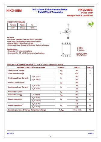
N-Channel Enhancement Mode PKC26BBNIKO-SEM Field Effect Transistor PDFN 5x6PHalogen-Free & Lead-FreePRODUCT SUMMARY V(BR)DSS RDS(ON) ID4 D30V 1.6m 151A GFeatures S Pb-Free, Halogen Free and RoHS compliant. Low RDS(on) to Minimize Conduction Losses. D D D D Ohmic Region Good RDS(on) Ratio. Optimized Gate Charge to Minimize Switching Losses. G. GATE D. DRAIN Applications S. SOURCE Protection Circuits Applications. Computer for DC to DC Converters Applications. 100% UIS Tested 100% Rg Tested #1 S S S GABSOLUTE MAXIMUM RATINGS (TA = 25 C Unless Otherwise Noted) PARAMETERS/TEST CONDITIONS SYMBOL LIMITS UNITSDrain-Source Voltage VDS 30 VGate-Source Voltage VGS 20 VTC = 25 C 151 Continuous Drain Current4 ID TC = 100 C 95 Pulsed Drain Current1 IDM 200A TA = 25 C 36 Continuous Drain Cu
Keywords - ALL TRANSISTORS DATASHEET
pkc26bb.pdf Design, MOSFET, Power
pkc26bb.pdf RoHS Compliant, Service, Triacs, Semiconductor
pkc26bb.pdf Database, Innovation, IC, Electricity


Liste
Recientemente añadidas las descripciónes de los transistores:
BJT: GA1A4M | SBT42 | 2SA200-Y | 2SA200-O | 2SD882-Q | 2SD882-P | 2SD882-E | 2SC945-L | 2SC945-H | 2SC4226-R23 | 2SC3357-F | 2SC3357-E | 2SC3356-R26 | 2SC3356-R24 | 2SC3356-R23 | 2SB772-Q | 2SB772-P | 2SB772-E | 2SA1015-L | 2SA1015-H | HSS8550
Popular searches
irfz44n | irf3205 | irfz44n datasheet | 2n4401 | bc547 transistor | bd139 | 2n4401 datasheet