spw15n60cfd.pdf datasheet:
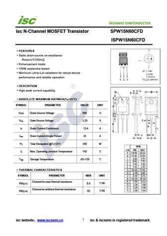
INCHANGE Semiconductorisc N-Channel MOSFET Transistor SPW15N60CFDISPW15N60CFDFEATURESStatic drain-source on-resistance:RDS(on)330mEnhancement mode:100% avalanche testedMinimum Lot-to-Lot variations for robust deviceperformance and reliable operationDESCRITIONHigh peak current capabilityABSOLUTE MAXIMUM RATINGS(T =25)aSYMBOL PARAMETER VALUE UNITV Drain-Source Voltage 600 VDSSV Gate-Source Voltage 20 VGSI Drain Current-Continuous 13.4 ADI Drain Current-Single Pulsed 33 ADMP Total Dissipation @T =25 240 WD CT Max. Operating Junction Temperature 150 jStorage Temperature -55~150 TstgTHERMAL CHARACTERISTICSSYMBOL PARAMETER MAX UNITChannel-to-case thermal resistance/WRth(j-c) 0.8Channel-to-ambient thermal resistance/WRth(j-a) 621isc websitewww.iscsemi.cn isc & iscsemi
Keywords - ALL TRANSISTORS DATASHEET
spw15n60cfd.pdf Design, MOSFET, Power
spw15n60cfd.pdf RoHS Compliant, Service, Triacs, Semiconductor
spw15n60cfd.pdf Database, Innovation, IC, Electricity


Liste
Recientemente añadidas las descripciónes de los transistores:
BJT: GA1A4M | SBT42 | 2SA200-Y | 2SA200-O | 2SD882-Q | 2SD882-P | 2SD882-E | 2SC945-L | 2SC945-H | 2SC4226-R23 | 2SC3357-F | 2SC3357-E | 2SC3356-R26 | 2SC3356-R24 | 2SC3356-R23 | 2SB772-Q | 2SB772-P | 2SB772-E | 2SA1015-L | 2SA1015-H | HSS8550
Popular searches
irfz44n | irf3205 | irfz44n datasheet | 2n4401 | bc547 transistor | bd139 | 2n4401 datasheet