APT35GT120JU2 IGBT Equivalente. Reemplazo. Hoja de especificaciones. Principales características
Número de Parte: APT35GT120JU2
Tipo de transistor: IGBT
Polaridad de transistor: N
ESPECIFICACIONES TECNICAS
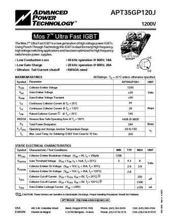
Pcⓘ - Máxima potencia disipada: 260 W
|Vce|ⓘ - Tensión máxima colector-emisor: 1200 V
|Vge|ⓘ - Tensión máxima puerta-emisor: 20 V
|Ic|ⓘ - Colector de Corriente Continua a 25℃: 55 A
Tjⓘ -
Temperatura máxima de unión: 150 ℃
CARACTERÍSTICAS ELÉCTRICAS
|VCEsat|ⓘ -
Voltaje de saturación colector-emisor, typ: 1.7 V @25℃
trⓘ - Tiempo de subida, typ: 30 nS
Coesⓘ - Capacitancia de salida, typ: 132 pF
Encapsulados: SOT227
Búsqueda de reemplazo de APT35GT120JU2 IGBT
- Selección ⓘ de transistores por parámetros
APT35GT120JU2 datasheet
..1. Size:606K apt
apt35gt120ju2.pdf 
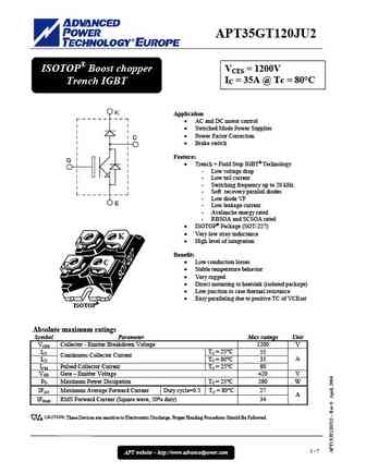
APT35GT120JU2 ISOTOP Boost chopper VCES = 1200V IC = 35A @ Tc = 80 C Trench IGBT K Application AC and DC motor control Switched Mode Power Supplies Power Factor Correction C Brake switch Features G Trench + Field Stop IGBT Technology - Low voltage drop - Low tail current - Switching frequency up to 20 kHz - Soft recovery parallel diodes -
2.1. Size:606K apt
apt35gt120ju3.pdf
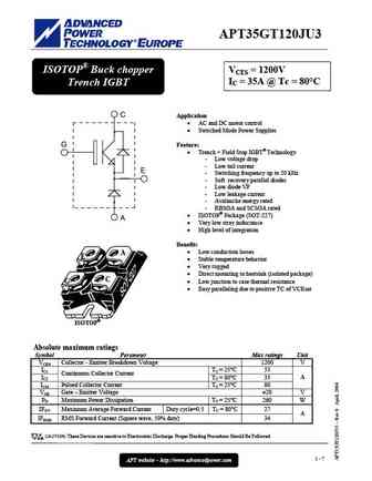
APT35GT120JU3 ISOTOP Buck chopper VCES = 1200V IC = 35A @ Tc = 80 C Trench IGBT C Application AC and DC motor control Switched Mode Power Supplies G Features Trench + Field Stop IGBT Technology - Low voltage drop - Low tail current E - Switching frequency up to 20 kHz - Soft recovery parallel diodes - Low diode VF - Low leakage current - Avalanche
8.1. Size:419K apt
apt35gp120b2dq2g.pdf
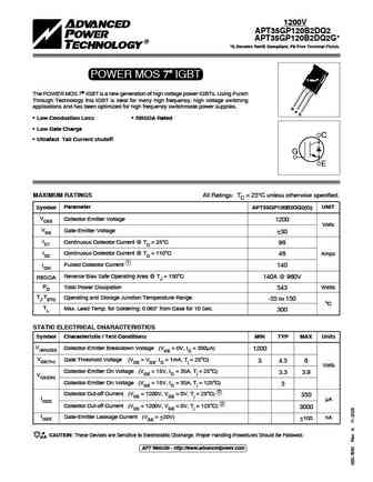
TYPICAL PERFORMANCE CURVES APT35GP120B2DQ2(G) 1200V APT35GP120B2DQ2 APT35GP120B2DQ2G* *G Denotes RoHS Compliant, Pb Free Terminal Finish. POWER MOS 7 IGBT T-Max The POWER MOS 7 IGBT is a new generation of high voltage power IGBTs. Using Punch Through Technology this IGBT is ideal for many high frequency, high voltage switching applications and has been optimized for hi
8.2. Size:202K apt
apt35gp120jdf2.pdf
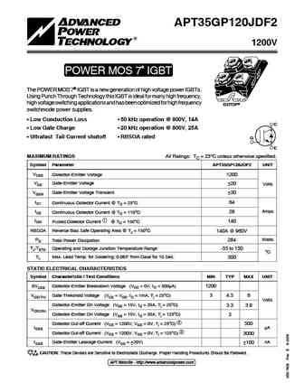
TYPICAL PERFORMANCE CURVES APT35GP120JDF2 APT35GP120JDF2 1200V POWER MOS 7 IGBT The POWER MOS 7 IGBT is a new generation of high voltage power IGBTs. Using Punch Through Technology this IGBT is ideal for many high frequency, "UL Recognized" high voltage switching applications and has been optimized for high frequency ISOTOP switchmode power supplies. Low Conduction Loss
8.4. Size:194K apt
apt35gp120b2df2.pdf

TYPICAL PERFORMANCE CURVES APT35GP120B2DF2 APT35GP120B2DF2 1200V POWER MOS 7 IGBT T-MaxTM The POWER MOS 7 IGBT is a new generation of high voltage power IGBTs. Using Punch Through Technology this IGBT is ideal for many high frequency, high voltage switching applications and has been optimized for high frequency switchmode power supplies. G C E Low Conduction Loss 100
8.5. Size:85K apt
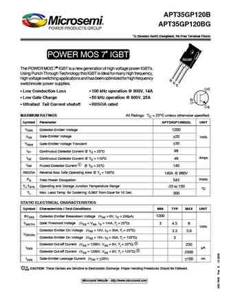
apt35gp120b.pdf
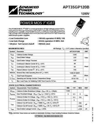
APT35GP120B 1200V POWER MOS 7 IGBT TO-247 The POWER MOS 7 IGBT is a new generation of high voltage power IGBTs. Using Punch Through Technology this IGBT is ideal for many high frequency, high voltage switching applications and has been optimized for high frequency G C switchmode power supplies. E C Low Conduction Loss 100 kHz operation @ 800V, 14A Low Gate Charge
8.6. Size:451K apt
apt35gp120jdq2.pdf
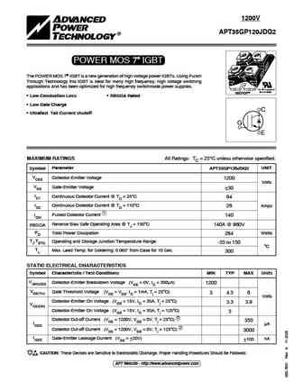
TYPICAL PERFORMANCE CURVES APT35GP120JDQ2 1200V APT35GP120JDQ2 POWER MOS 7 IGBT The POWER MOS 7 IGBT is a new generation of high voltage power IGBTs. Using Punch Through Technology this IGBT is ideal for many high frequency, high voltage switching applications and has been optimized for high frequency switchmode power supplies. "UL Recognized" ISOTOP file # E145592
8.7. Size:237K apt
apt35gn120l2dq2g.pdf
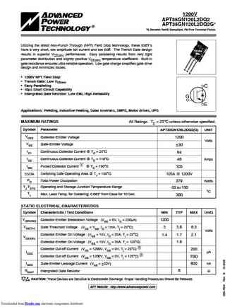
TYPICAL PERFORMANCE CURVES APT35GN120L2DQ2(G) 1200V APT35GN120L2DQ2 APT35GN120L2DQ2G* *G Denotes RoHS Compliant, Pb Free Terminal Finish. Utilizing the latest Non-Punch Through (NPT) Field Stop technology, these IGBT s have a very short, low amplitude tail current and low Eoff. The Trench Gate design TO-264 Max results in superior VCE(on) performance. Easy paralleling result
8.8. Size:180K apt
apt35gn120b.pdf
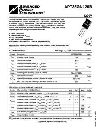
TYPICAL PERFORMANCE CURVES APT35GN120B APT35GN120B 1200V Utilizing the latest Field Stop technology, these IGBT s have a very short, low amplitude tail current and low Eoff. The Trench Gate design results in superior VCE(on) performance. Easy paralleling results from very tight parameter distribution and slightly positive VCE(on) temperature coefficient. Built-in gate resistance en
8.9. Size:238K microsemi
apt35ga90sd15.pdf
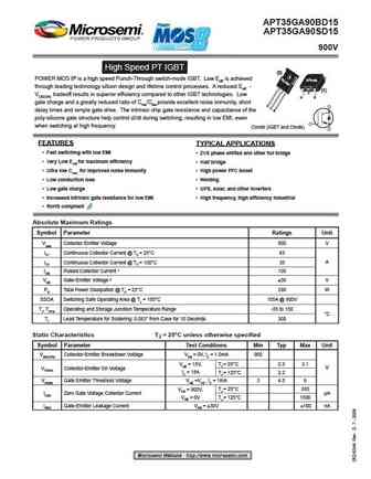
APT35GA90BD15 APT35GA90SD15 900V High Speed PT IGBT (B) POWER MOS 8 is a high speed Punch-Through switch-mode IGBT. Low Eoff is achieved D3PAK through leading technology silicon design and lifetime control processes. A reduced Eoff - (S) C VCE(ON) tradeoff results in superior efficiency compared to other IGBT technologies. Low G E gate charge and a greatly reduced ratio of C
8.10. Size:257K microsemi
apt35gp120bg.pdf
APT35GP120B APT35GP120BG *G Denotes RoHS Compliant, Pb Free Terminal Finish. POWER MOS 7 IGBT TO-247 The POWER MOS 7 IGBT is a new generation of high voltage power IGBTs. Using Punch Through Technology this IGBT is ideal for many high frequency, high voltage switching applications and has been optimized for high frequency G C switchmode power supplies. E C Low Conduction
8.11. Size:238K microsemi
apt35ga90bd15.pdf
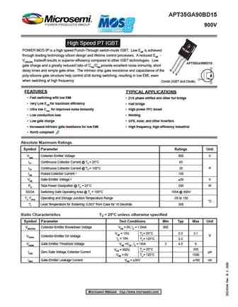
APT35GA90BD15 900V High Speed PT IGBT POWER MOS 8 is a high speed Punch-Through switch-mode IGBT. Low Eoff is achieved through leading technology silicon design and lifetime control processes. A reduced Eoff - VCE(ON) tradeoff results in superior efficiency compared to other IGBT technologies. Low APT35GA90BD15 gate charge and a greatly reduced ratio of Cres/Cies provide excellent
8.12. Size:207K microsemi
apt35ga90s.pdf
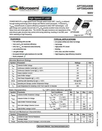
APT35GA90B APT35GA90S 900V High Speed PT IGBT APT35GA90S POWER MOS 8 is a high speed Punch-Through switch-mode IGBT. Low Eoff is achieved through leading technology silicon design and lifetime control processes. A reduced Eoff - D3PAK VCE(ON) tradeoff results in superior efficiency compared to other IGBT technologies. Low gate charge and a greatly reduced ratio of Cres/Cies pro
8.13. Size:142K microsemi
apt35gn120sg.pdf

TYPICAL PERFORMANCE CURVES APT35GN120B_S(G) APT35GN120B APT35GN120S APT35GN120BG APT35GN120SG 1200V *G Denotes RoHS Compliant, Pb Free Terminal Finish. Utilizing the latest Non-Punch Through (NPT) Field Stop technology, these IGBT s (B) have a very short, low amplitude tail current and low Eoff. The Trench Gate design D3PAK results in superior VCE(on) performance. Easy paralle
8.14. Size:142K microsemi
apt35gn120bg.pdf
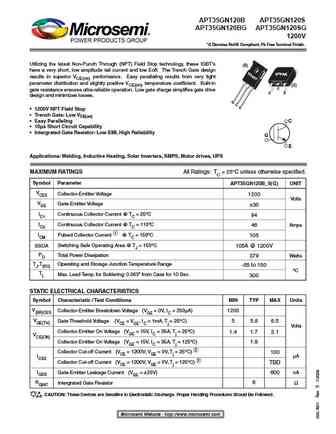
TYPICAL PERFORMANCE CURVES APT35GN120B_S(G) APT35GN120B APT35GN120S APT35GN120BG APT35GN120SG 1200V *G Denotes RoHS Compliant, Pb Free Terminal Finish. Utilizing the latest Non-Punch Through (NPT) Field Stop technology, these IGBT s (B) have a very short, low amplitude tail current and low Eoff. The Trench Gate design D3PAK results in superior VCE(on) performance. Easy paralle
8.15. Size:117K microsemi
apt35ga90b.pdf
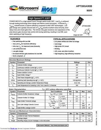
APT35GA90B 900V High Speed PT IGBT POWER MOS 8 is a high speed Punch-Through switch-mode IGBT. Low Eoff is achieved through leading technology silicon design and lifetime control processes. A reduced Eoff - VCE(ON) tradeoff results in superior efficiency compared to other IGBT technologies. Low APT35GA90B gate charge and a greatly reduced ratio of Cres/Cies provide excellent noise
Otros transistores... APT33GF120B2RD
, APT33GF120BR
, APT33GF120HR
, APT35GN120B
, APT35GP120B
, APT35GP120B2DF2
, APT35GP120J
, APT35GP120JDF2
, CRG60T60AK3HD
, APT35GT120JU3
, APT40GF120JRD
, APT40GP60B
, APT40GP60B2DF2
, APT40GP60J
, APT40GP60JDF2
, APT40GP90B
, APT40GP90B2DF2
.