APT102GA60L IGBT Equivalente. Reemplazo. Hoja de especificaciones. Principales características
Número de Parte: APT102GA60L
Tipo de transistor: IGBT
Polaridad de transistor: N
ESPECIFICACIONES TECNICAS
Pcⓘ - Máxima potencia disipada: 780 W
|Vce|ⓘ - Tensión máxima colector-emisor: 600 V
|Vge|ⓘ - Tensión máxima puerta-emisor: 30 V
|Ic|ⓘ - Colector de Corriente Continua a 25℃: 102 A
Tjⓘ - Temperatura máxima de unión: 150 ℃
CARACTERÍSTICAS ELÉCTRICAS
|VCEsat|ⓘ - Voltaje de saturación colector-emisor, typ: 1.9 V @25℃
trⓘ - Tiempo de subida, typ: 37 nS
Coesⓘ - Capacitancia de salida, typ: 630 pF
Encapsulados: TO264
Búsqueda de reemplazo de APT102GA60L IGBT
- Selección ⓘ de transistores por parámetros
APT102GA60L datasheet
apt102ga60l.pdf
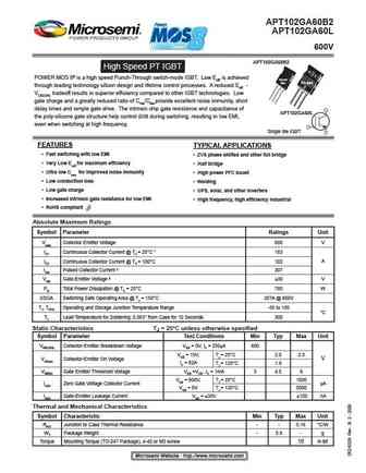
APT102GA60B2 APT102GA60L 600V APT102GA60B2 High Speed PT IGBT POWER MOS 8 is a high speed Punch-Through switch-mode IGBT. Low Eoff is achieved through leading technology silicon design and lifetime control processes. A reduced Eoff - VCE(ON) tradeoff results in superior efficiency compared to other IGBT technologies. Low gate charge and a greatly reduced ratio of Cres/Cies prov
apt102ga60b2.pdf

APT102GA60B2 APT102GA60L 600V APT102GA60B2 High Speed PT IGBT POWER MOS 8 is a high speed Punch-Through switch-mode IGBT. Low Eoff is achieved through leading technology silicon design and lifetime control processes. A reduced Eoff - VCE(ON) tradeoff results in superior efficiency compared to other IGBT technologies. Low gate charge and a greatly reduced ratio of Cres/Cies prov
apt100gf60b2r apt100gf60lr.pdf
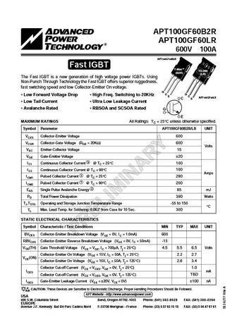
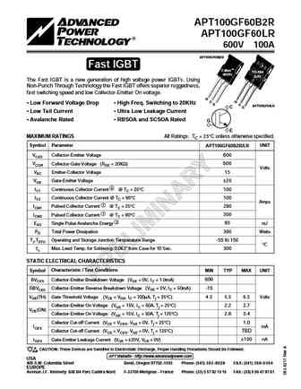
APT100GF60B2R APT100GF60LR 600V 100A APT100GF60B2R Fast IGBT T-Max TO-264 (B2R) (LR) The Fast IGBT is a new generation of high voltage power IGBTs. Using Non-Punch Through Technology the Fast IGBT offers superior ruggedness, fast switching speed and low Collector-Emitter On voltage. G C G Low Forward Voltage Drop High Freq. Switching to 20KHz E C APT100GF60LR C E
apt10040b2vfr.pdf

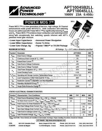
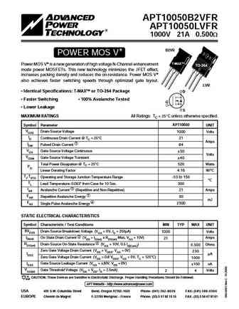
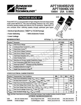
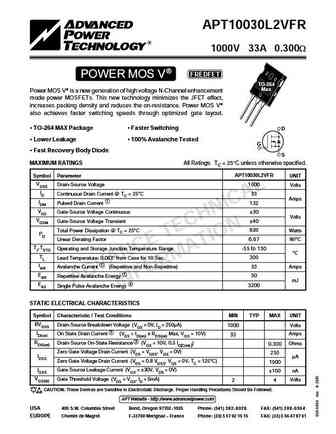
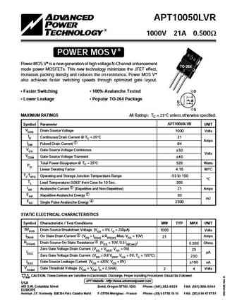
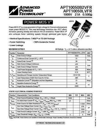
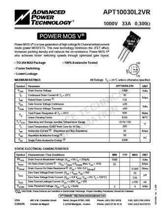
APT10040B2VFR APT10040LVFR 1000V 25A 0.400W B2VFR POWER MOS V FREDFET T-MAX Power MOS V is a new generation of high voltage N-Channel enhancement TO-264 mode power MOSFETs. This new technology minimizes the JFET effect, increases packing density and reduces the on-resistance. Power MOS V also achieves faster switching speeds through optimized gate layout. LVFR Identical
apt10057wvr.pdf
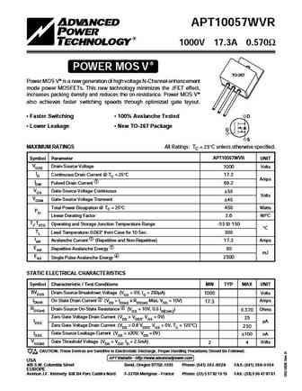
APT10057WVR 1000V 17.3A 0.570 POWER MOS V TO-267 Power MOS V is a new generation of high voltage N-Channel enhancement mode power MOSFETs. This new technology minimizes the JFET effect, increases packing density and reduces the on-resistance. Power MOS V also achieves faster switching speeds through optimized gate layout. Faster Switching 100% Avalanche Tested D Lo
apt10045b2llg apt10045lllg.pdf
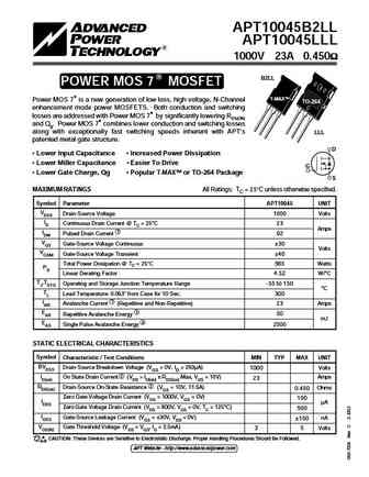
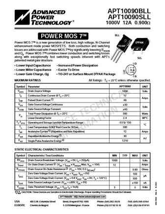
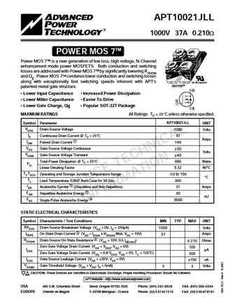
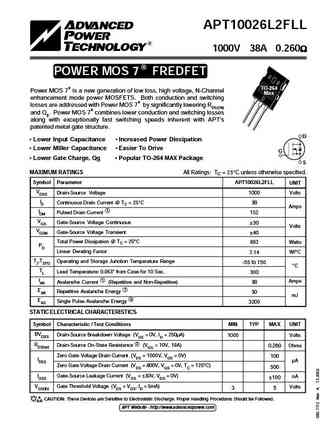
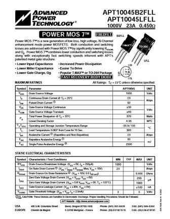
APT10045B2LL APT10045LLL 1000V 23A 0.450 R B2LL POWER MOS 7 MOSFET T-MAX Power MOS 7 is a new generation of low loss, high voltage, N-Channel TO-264 enhancement mode power MOSFETS. Both conduction and switching losses are addressed with Power MOS 7 by significantly lowering RDS(ON) and Qg. Power MOS 7 combines lower conduction and switching losses al
apt10m07jvfr.pdf
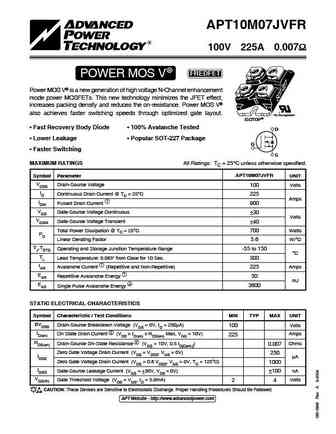
APT10M07JVFR 100V 225A 0.007 POWER MOS V FREDFET Power MOS V is a new generation of high voltage N-Channel enhancement mode power MOSFETs. This new technology minimizes the JFET effect, increases packing density and reduces the on-resistance. Power MOS V also achieves faster switching speeds through optimized gate layout. "UL Recognized" ISOTOP Fast R
apt10m07.pdf

APT10M07JVR 100V 225A 0.007 POWER MOS V Power MOS V is a new generation of high voltage N-Channel enhancement mode power MOSFETs. This new technology minimizes the JFET effect, increases packing density and reduces the on-resistance. Power MOS V also achieves faster switching speeds through optimized gate layout. "UL Recognized" ISOTOP Faster Switching 100% Avalanche
apt10050jn.pdf
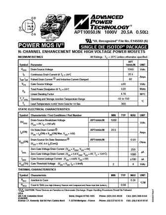
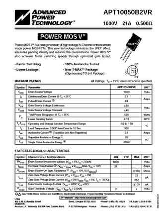
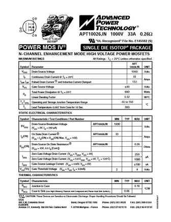
D G APT10050JN 1000V 20.5A 0.50 S ISOTOP "UL Recognized" File No. E145592 (S) POWER MOS IV SINGLE DIE ISOTOP PACKAGE N- CHANNEL ENHANCEMENT MODE HIGH VOLTAGE POWER MOSFETS MAXIMUM RATINGS All Ratings TC = 25 C unless otherwise specified. APT Symbol Parameter 10050JN UNIT VDSS Drain-Source Voltage 1000 Volts ID Continuous Drain Current @ TC = 25 C 20.5 Amps IDM, lLM
apt10090bfllg apt10090sfllg.pdf
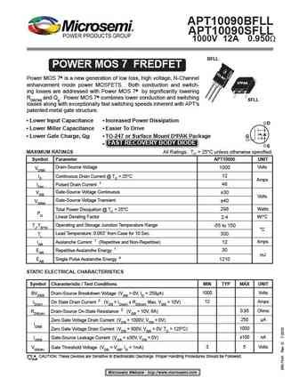
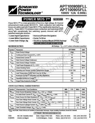
APT10090BFLL APT10090SFLL 1000V 12A 0.950 BFLL POWER MOS 7 FREDFET Power MOS 7 is a new generation of low loss, high voltage, N-Channel D3PAK enhancement mode power MOSFETS. Both conduction and switch- ing losses are addressed with Power MOS 7 by significantly lowering RDS(ON) and Qg. Power MOS 7 combines lower conduction and switching SFLL losses along with exceptiona
apt10m09b2vr.pdf

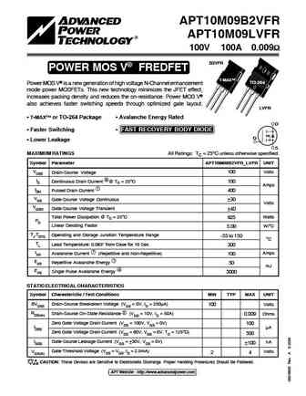
APT10M09B2VR APT10M09LVR 100V 100A 0.009W B2VR POWER MOS V T-MAX Power MOS V is a new generation of high voltage N-Channel enhancement TO-264 mode power MOSFETs. This new technology minimizes the JFET effect, increases packing density and reduces the on-resistance. Power MOS V also achieves faster switching speeds through optimized gate layout. LVR Identical Specificati
apt100gf60ju3.pdf
APT100GF60JU3 ISOTOP Buck chopper VCES = 600V IC = 100A @ Tc = 80 C NPT IGBT C Application AC and DC motor control Switched Mode Power Supplies G Features Non Punch Through (NPT) THUNDERBOLT IGBT E - Low voltage drop - Low tail current - Switching frequency up to 100 kHz - Soft recovery parallel diodes - Low diode VF - Low leakage current A - Aval
apt10m07jvr.pdf

APT10M07JVR 100V 225A 0.007 POWER MOS V Power MOS V is a new generation of high voltage N-Channel enhancement mode power MOSFETs. This new technology minimizes the JFET effect, increases packing density and reduces the on-resistance. Power MOS V also achieves faster switching speeds through optimized gate layout. "UL Recognized" ISOTOP Faster Switching 100% Avalanche
apt10m09lvfrg.pdf
APT10M09B2VFR APT10M09LVFR 100V 100A 0.009 B2VFR POWER MOS V FREDFET T-MAX TO-264 Power MOS V is a new generation of high voltage N-Channel enhancement mode power MOSFETs. This new technology minimizes the JFET effect, increases packing density and reduces the on-resistance. Power MOS V also achieves faster switching speeds through optimized gate layou
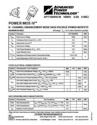
apt1002rcn.pdf

D TO-254 G APT1002RCN 1000V 5.5A 2.00 S TM POWER MOS IV N - CHANNEL ENHANCEMENT MODE HIGH VOLTAGE POWER MOSFETS MAXIMUM RATINGS All Ratings TC = 25 C unless otherwise specified. Symbol Parameter APT1002RCN UNIT VDSS Drain-Source Voltage 1000 Volts ID Continuous Drain Current @ TC = 25 C 5.5 Amps IDM Pulsed Drain Current 1 22 VGS Gate-Source Voltage 30 Volts Total Powe
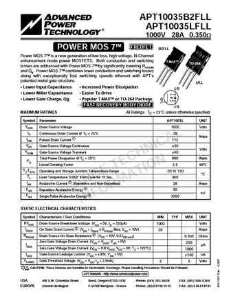
apt10035jfll.pdf

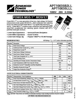
APT10035JFLL 1000V 25A 0.350W TM FREDFET POWER MOS 7 Power MOS 7TM is a new generation of low loss, high voltage, N-Channel enhancement mode power MOSFETS. Both conduction and switching losses are addressed with Power MOS 7TM by significantly lowering RDS(ON) and Qg. Power MOS 7TM combines lower conduction and switching losses along with exceptionally fast switching speeds inherent wi
apt100gn120j.pdf
TYPICAL PERFORMANCE CURVES APT100GN120J 1200V APT100GN120J Utilizing the latest Field Stop and Trench Gate technologies, these IGBT's have ultra low VCE(ON) and are ideal for low frequency applications that require absolute minimum conduction loss. Easy paralleling is a result of very tight parameter distribution and a slightly positive VCE(ON) temperature coefficient. A built-in
apt1001r1avr.pdf
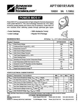
APT1001R1AVR 1000V 9A 1.100 POWER MOS V TO-3 Power MOS V is a new generation of high voltage N-Channel enhancement mode power MOSFETs. This new technology minimizes the JFET effect, increases packing density and reduces the on-resistance. Power MOS V also achieves faster switching speeds through optimized gate layout. D Faster Switching 100% Avalanche Tested Lower
apt10078bfll.pdf

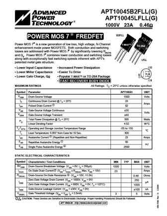
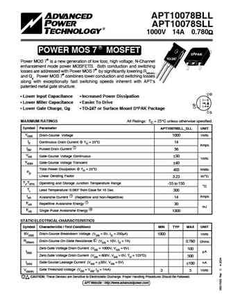
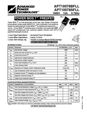
APT10078BFLL APT10078SFLL 1000V 14A 0.780W TM BFLL FREDFET POWER MOS 7 Power MOS 7TM is a new generation of low loss, high voltage, N-Channel D3PAK TO-247 enhancement mode power MOSFETS. Both conduction and switching losses are addressed with Power MOS 7TM by significantly lowering RDS(ON) and Qg. Power MOS 7TM combines lower conduction and switching losses along with exceptionally
apt10078bll.pdf
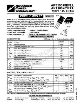
APT10078BLL APT10078SLL 1000V 14A 0.780W TM BLL POWER MOS 7 Power MOS 7TM is a new generation of low loss, high voltage, N-Channel D3PAK TO-247 enhancement mode power MOSFETS. Both conduction and switching losses are addressed with Power MOS 7TM by significantly lowering RDS(ON) and Qg. Power MOS 7TM combines lower conduction and switching losses along with exceptionally fast switchi
apt1001rblc.pdf

APT1001RBLC APT1001RSLC 1000V 11A 1.000W BLC TM POWER MOS VI D3PAK Power MOS VITM is a new generation of low gate charge, high voltage TO-247 N-Channel enhancement mode power MOSFETs. Lower gate charge is achieved by optimizing the manufacturing process to minimize Ciss and Crss. Lower gate charge coupled with Power MOS VITM optimized gate layout, SLC delivers exceptionally fast sw
apt10090bllg apt10090sllg.pdf
APT10090BLL APT10090SLL 1000V 12A 0.950 BLL POWER MOS 7 MOSFET Power MOS 7 is a new generation of low loss, high voltage, N-Channel D3PAK enhancement mode power MOSFETS. Both conduction and switch- ing losses are addressed with Power MOS 7 by significantly lowering RDS(ON) and Qg. Power MOS 7 combines lower conduction and switching SLL losses along with exceptionally fa
apt1004.pdf
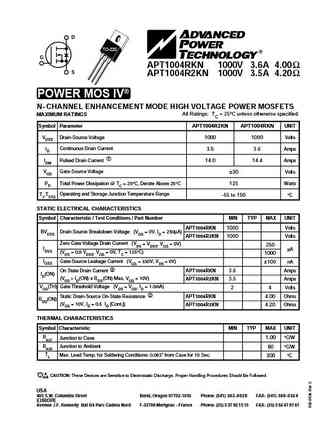
D TO-254 G APT1004RCN 1000V 3.6A 4.00 S TM POWER MOS IV N - CHANNEL ENHANCEMENT MODE HIGH VOLTAGE POWER MOSFETS MAXIMUM RATINGS All Ratings TC = 25 C unless otherwise specified. Symbol Parameter APT1004RCN UNIT VDSS Drain-Source Voltage 1000 Volts ID Continuous Drain Current @ TC = 25 C 3.6 Amps IDM Pulsed Drain Current 1 14.4 VGS Gate-Source Voltage 30 Volts Total Po
apt1001rsvrg.pdf
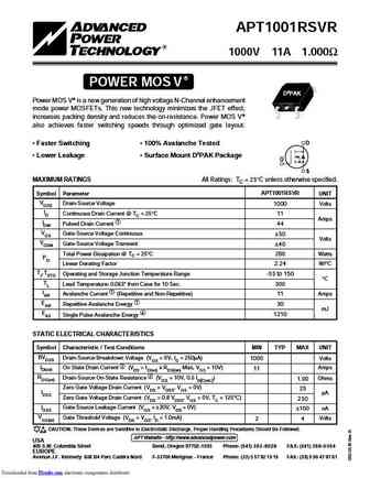
APT1001RSVR 1000V 11A 1.000 POWER MOS V D3PAK Power MOS V is a new generation of high voltage N-Channel enhancement mode power MOSFETs. This new technology minimizes the JFET effect, increases packing density and reduces the on-resistance. Power MOS V also achieves faster switching speeds through optimized gate layout. D Faster Switching 100% Avalanche Tested Lowe
apt1004rgn.pdf
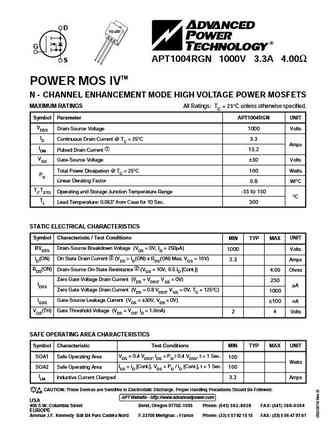
D TO-257 G APT1004RGN 1000V 3.3A 4.00 S TM POWER MOS IV N - CHANNEL ENHANCEMENT MODE HIGH VOLTAGE POWER MOSFETS MAXIMUM RATINGS All Ratings TC = 25 C unless otherwise specified. Symbol Parameter APT1004RGN UNIT VDSS Drain-Source Voltage 1000 Volts ID Continuous Drain Current @ TC = 25 C 3.3 Amps IDM Pulsed Drain Current 1 13.2 VGS Gate-Source Voltage 30 Volts Total Po
apt10035jll.pdf

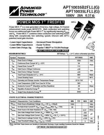
APT10035JLL 1000V 25A 0.350 W TM POWER MOS 7 Power MOS 7TM is a new generation of low loss, high voltage, N-Channel enhancement mode power MOSFETS. Both conduction and switching losses are addressed with Power MOS 7TM by significantly lowering RDS(ON) and Qg. Power MOS 7TM combines lower conduction and switching losses along with exceptionally fast switching speeds inherent with APT's
apt10m30avr.pdf

APT10M30AVR 100V 65A 0.030 POWER MOS V Power MOS V is a new generation of high voltage N-Channel enhancement mode power MOSFETs. This new technology minimizes the JFET effect, increases packing density and reduces the on-resistance. Power MOS V also achieves faster switching speeds through optimized gate layout. D Faster Switching 100% Avalanche Tested Lower Leakag
apt10035b2fll.pdf
APT10035B2FLL APT10035LFLL 1000V 28A 0.350W TM FREDFET POWER MOS 7 B2FLL Power MOS 7TM is a new generation of low loss, high voltage, N-Channel enhancement mode power MOSFETS. Both conduction and switching T-MAX TO-264 losses are addressed with Power MOS 7TM by significantly lowering RDS(ON) and Qg. Power MOS 7TM combines lower conduction and switching losses along with excepti
apt100gf60jr.pdf
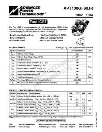
APT100GF60JR 600V 100A Fast IGBT The Fast IGBT is a new generation of high voltage power IGBTs. Using Non-Punch Through Technology the Fast IGBT offers superior ruggedness, fast switching speed and low Collector-Emitter On voltage. "UL Recognized" Low Forward Voltage Drop High Freq. Switching to 20KHz ISOTOP C Low Tail Current Ultra Low Leakage Current Avalanche
apt10045b2ll.pdf
APT10045B2LL APT10045LLL 1000V 23A 0.450W B2LL TM POWER MOS 7 Power MOS 7TM is a new generation of low loss, high voltage, N-Channel T-MAX TO-264 enhancement mode power MOSFETS. Both conduction and switching losses are addressed with Power MOS 7TM by significantly lowering RDS(ON) and Qg. Power MOS 7TM combines lower conduction and switching losses along with exceptionally fast
apt10090bll.pdf
APT10090BLL APT10090SLL 1000V 12A 0.900W TM BLL POWER MOS 7 Power MOS 7TM is a new generation of low loss, high voltage, N-Channel D3PAK TO-247 enhancement mode power MOSFETS. Both conduction and switching losses are addressed with Power MOS 7TM by significantly lowering RDS(ON) and Qg. Power MOS 7TM combines lower conduction and switching losses along with exceptionally fast switchi
apt10090bfll.pdf
APT10090BFLL APT10090SFLL 1000V 12A 0.900W TM BFLL FREDFET POWER MOS 7 Power MOS 7TM is a new generation of low loss, high voltage, N-Channel D3PAK TO-247 enhancement mode power MOSFETS. Both conduction and switching losses are addressed with Power MOS 7TM by significantly lowering RDS(ON) and Qg. Power MOS 7TM combines lower conduction and switching losses along with exceptionally
apt10021jll.pdf
APT10021JLL 1000V 37A 0.210W TM POWER MOS 7 Power MOS 7TM is a new generation of low loss, high voltage, N-Channel enhancement mode power MOSFETS. Both conduction and switching losses are addressed with Power MOS 7TM by significantly lowering RDS(ON) and Qg. Power MOS 7TM combines lower conduction and switching losses along with exceptionally fast switching speeds inherent with APT's
apt10m19bvr.pdf

APT10M19BVR 100V 75A 0.019 POWER MOS V Power MOS V is a new generation of high voltage N-Channel enhancement TO-247 mode power MOSFETs. This new technology minimizes the JFET effect, increases packing density and reduces the on-resistance. Power MOS V also achieves faster switching speeds through optimized gate layout. Faster Switching 100% Avalanche Tested D Lower
apt10045b2fllg apt10045lfllg.pdf
APT10045B2FLL APT10045LFLL 1000V 23A 0.4 R B2FLL POWER MOS 7 FREDFET Power MOS 7 is a new generation of low loss, high voltage, N-Channel T-MAX TO-264 enhancement mode power MOSFETS. Both conduction and switching losses are addressed with Power MOS 7 by significantly lowering RDS(ON) and Qg. Power MOS 7 combines lower conduction and switching l
apt10078sfll.pdf
APT10078BFLL APT10078SFLL 1000V 14A 0.780W TM BFLL FREDFET POWER MOS 7 Power MOS 7TM is a new generation of low loss, high voltage, N-Channel D3PAK TO-247 enhancement mode power MOSFETS. Both conduction and switching losses are addressed with Power MOS 7TM by significantly lowering RDS(ON) and Qg. Power MOS 7TM combines lower conduction and switching losses along with exceptionally
apt1001r1bvfr.pdf

APT1001R1BVFR 1000V 11A 1.100 POWER MOS V FREDFET Power MOS V is a new generation of high voltage N-Channel enhancement TO-247 mode power MOSFETs. This new technology minimizes the JFET effect, increases packing density and reduces the on-resistance. Power MOS V also achieves faster switching speeds through optimized gate layout. Fast Recovery Body Diode 100% Avalanche T
apt10078bllg apt10078sllg.pdf
APT10078BLL APT10078SLL 1000V 14A 0.780 R POWER MOS 7 MOSFET D3PAK TO-247 Power MOS 7 is a new generation of low loss, high voltage, N-Channel enhancement mode power MOSFETS. Both conduction and switching losses are addressed with Power MOS 7 by significantly lowering RDS(ON) and Qg. Power MOS 7 combines lower conduction and switching losses along with e
apt1001rbvr.pdf

APT1001RBVR 1000V 11A 1.000 POWER MOS V Power MOS V is a new generation of high voltage N-Channel enhancement TO-247 mode power MOSFETs. This new technology minimizes the JFET effect, increases packing density and reduces the on-resistance. Power MOS V also achieves faster switching speeds through optimized gate layout. D Faster Switching 100% Avalanche Tested Lowe
apt1003rbfllg apt1003rsfllg.pdf
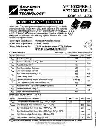
APT1003RBFLL APT1003RSFLL 1000V 4A 3.00 R POWER MOS 7 FREDFET D3PAK TO-247 Power MOS 7 is a new generation of low loss, high voltage, N-Channel enhancement mode power MOSFETS. Both conduction and switching losses are addressed with Power MOS 7 by significantly lowering RDS(ON) and Qg. Power MOS 7 combines lower conduction and switching losses along with
apt100f50j.pdf
APT100F50J 500V, 103A, 0.036 Max, trr 390ns N-Channel FREDFET Power MOS 8 is a high speed, high voltage N-channel switch-mode power MOSFET. A proprietary planar stripe design yields excellent reliability and manufacturability. Low switching loss is achieved with low input capacitance and ultra low Crss "Miller" capaci- tance. The intrinsic gate resistance and capacitance of th
apt10m19bvrg.pdf
APT10M19BVR 100V 75A 0.019 POWER MOS V Power MOS V is a new generation of high voltage N-Channel enhancement TO-247 mode power MOSFETs. This new technology minimizes the JFET effect, increases packing density and reduces the on-resistance. Power MOS V also achieves faster switching speeds through optimized gate layout. Faster Switching 100% Avalanche Tested D Lower
apt10050b2vfr.pdf
APT10050B2VFR APT10050LVFR 1000V 21A 0.500W B2VR POWER MOS V T-MAX Power MOS V is a new generation of high voltage N-Channel enhancement TO-264 mode power MOSFETs. This new technology minimizes the JFET effect, increases packing density and reduces the on-resistance. Power MOS V also achieves faster switching speeds through optimized gate layout. LVR Identical Specifica
apt10040b2vr.pdf
APT10040B2VR APT10040LVR 1000V 25A 0.400W B2VR POWER MOS V T-MAX Power MOS V is a new generation of high voltage N-Channel enhancement TO-264 mode power MOSFETs. This new technology minimizes the JFET effect, increases packing density and reduces the on-resistance. Power MOS V also achieves faster switching speeds through optimized gate layout. LVR Identical Specificati
apt10040b2vfrg apt10040lvfrg.pdf

APT10040B2VFR APT10040LVFR 1000V 25A 0.400W B2VFR FREDFET POWER MOS V T-MAX Power MOS V is a new generation of high voltage N-Channel enhancement TO-264 mode power MOSFETs. This new technology minimizes the JFET effect, increases packing density and reduces the on-resistance. Power MOS V also achieves faster switching speeds through optimized gate layout. LVFR Identica
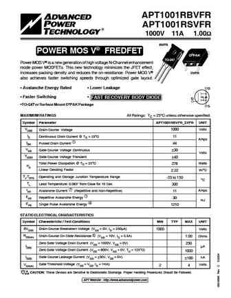
apt1001rbvfr.pdf

APT1001RBVFR APT1001RSVFR 1000V 11A 1.00 BVFR POWER MOS V FREDFET D3PAK TO-247 Power MOS V is a new generation of high voltage N-Channel enhancement mode power MOSFETs. This new technology minimizes the JFET effect, increases packing density and reduces the on-resistance. Power MOS V SVFR also achieves faster switching speeds through optimized gate layou
apt1001r1hvr.pdf
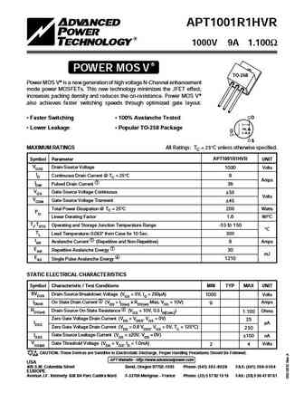
APT1001R1HVR 1000V 9A 1.100 POWER MOS V TO-258 Power MOS V is a new generation of high voltage N-Channel enhancement mode power MOSFETs. This new technology minimizes the JFET effect, increases packing density and reduces the on-resistance. Power MOS V also achieves faster switching speeds through optimized gate layout. D Faster Switching 100% Avalanche Tested Low
apt10035b2llg apt10035lllg.pdf
APT10035B2LL APT10035LLL 1000V 28A 0.350 R B2LL POWER MOS 7 MOSFET T-MAX Power MOS 7 is a new generation of low loss, high voltage, N-Channel TO-264 enhancement mode power MOSFETS. Both conduction and switching losses are addressed with Power MOS 7 by significantly lowering RDS(ON) and Qg. Power MOS 7 combines lower conduction and switching losses al
apt1001r6bn.pdf
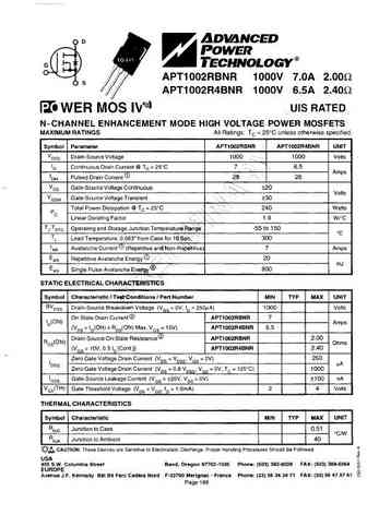
D TO-247 G APT1001R6BN 1000V 8.0A 1.60 S APT1002R4BN 1000V 6.5A 2.40 POWER MOS IV N- CHANNEL ENHANCEMENT MODE HIGH VOLTAGE POWER MOSFETS MAXIMUM RATINGS All Ratings TC = 25 C unless otherwise specified. APT APT Symbol Parameter 1001R6BN 1002R4BN UNIT VDSS Drain-Source Voltage 1000 1000 Volts ID Continuous Drain Current @ TC = 25 C 8 6.5 Amps IDM Pulsed Drain Current 1
apt1004rcn.pdf

D TO-254 G APT1004RCN 1000V 3.6A 4.00 S TM POWER MOS IV N - CHANNEL ENHANCEMENT MODE HIGH VOLTAGE POWER MOSFETS MAXIMUM RATINGS All Ratings TC = 25 C unless otherwise specified. Symbol Parameter APT1004RCN UNIT VDSS Drain-Source Voltage 1000 Volts ID Continuous Drain Current @ TC = 25 C 3.6 Amps IDM Pulsed Drain Current 1 14.4 VGS Gate-Source Voltage 30 Volts Total Po
apt10m19bvfr.pdf
APT10M19BVFR 100V 75A 0.019 POWER MOS V FREDFET TO-247 Power MOS V is a new generation of high voltage N-Channel enhancement TO-247 mode power MOSFETs. This new technology minimizes the JFET effect, increases packing density and reduces the on-resistance. Power MOS V also achieves faster switching speeds through optimized gate layout. Fast Recovery Body Diode 100% Avala
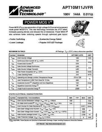
apt10m11jvr.pdf
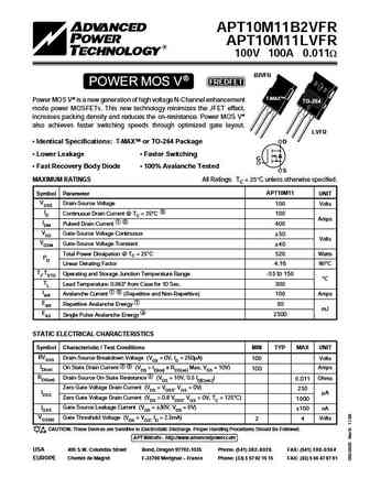
APT10M11JVR 100V 144A 0.011 POWER MOS V Power MOS V is a new generation of high voltage N-Channel enhancement mode power MOSFETs. This new technology minimizes the JFET effect, increases packing density and reduces the on-resistance. Power MOS V also achieves faster switching speeds through optimized gate layout. "UL Recognized" ISOTOP Faster Switching 100% Avalanche
apt10090sll.pdf

APT10090BLL APT10090SLL 1000V 12A 0.900W TM BLL POWER MOS 7 Power MOS 7TM is a new generation of low loss, high voltage, N-Channel D3PAK TO-247 enhancement mode power MOSFETS. Both conduction and switching losses are addressed with Power MOS 7TM by significantly lowering RDS(ON) and Qg. Power MOS 7TM combines lower conduction and switching losses along with exceptionally fast switchi
apt10050jlc.pdf

APT10050JLC 1000V 19A 0.500 TM POWER MOS VI Power MOS VITM is a new generation of low gate charge, high voltage N-Channel enhancement mode power MOSFETs. Lower gate charge is achieved by optimizing the manufacturing process to minimize Ciss and Crss. Lower gate charge coupled with Power MOS VITM optimized gate layout, "UL Recognized" delivers exceptionally fast s
apt10045jll.pdf
APT10045JLL 1000V 21A 0.450W TM POWER MOS 7 Power MOS 7TM is a new generation of low loss, high voltage, N-Channel enhancement mode power MOSFETS. Both conduction and switching losses are addressed with Power MOS 7TM by significantly lowering RDS(ON) and Qg. Power MOS 7TM combines lower conduction and switching losses along with exceptionally fast switching speeds inherent with APT's
apt10m11b2vr.pdf

APT10M11B2VR 100V 100A 0.011 POWER MOS V T-MAX Power MOS V is a new generation of high voltage N-Channel enhancement mode power MOSFETs. This new technology minimizes the JFET effect, increases packing density and reduces the on-resistance. Power MOS V also achieves faster switching speeds through optimized gate layout. Faster Switching 100% Avalanche Tested D L
apt10m09b2vfr.pdf

APT10M09B2VFR APT10M09LVFR 100V 100A 0.009W B2VFR POWER MOS V FREDFET T-MAX Power MOS V is a new generation of high voltage N-Channel enhancement TO-264 mode power MOSFETs. This new technology minimizes the JFET effect, increases packing density and reduces the on-resistance. Power MOS V also achieves faster switching speeds through optimized gate layout. LVFR Identical
apt10021jfll.pdf

APT10021JFLL 1000V 37A 0.210W TM FREDFET POWER MOS 7 Power MOS 7TM is a new generation of low loss, high voltage, N-Channel enhancement mode power MOSFETS. Both conduction and switching losses are addressed with Power MOS 7TM by significantly lowering RDS(ON) and Qg. Power MOS 7TM combines lower conduction and switching losses along with exceptionally fast switching speeds inherent wi
apt10m19svr.pdf

APT10M19SVR 100V 75A 0.019 POWER MOS V D3PAK Power MOS V is a new generation of high voltage N-Channel enhancement mode power MOSFETs. This new technology minimizes the JFET effect, increases packing density and reduces the on-resistance. Power MOS V also achieves faster switching speeds through optimized gate layout. D Faster Switching 100% Avalanche Tested Lower
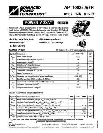
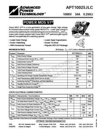
apt10025jvr.pdf
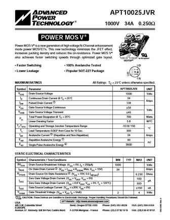
APT10025JVR 1000V 34A 0.250 POWER MOS V Power MOS V is a new generation of high voltage N-Channel enhancement mode power MOSFETs. This new technology minimizes the JFET effect, increases packing density and reduces the on-resistance. Power MOS V also achieves faster switching speeds through optimized gate layout. "UL Recognized" ISOTOP Faster Switching 100% Avalanche
apt10m25bvr.pdf

APT10M25BVR 100V 75A 0.025 POWER MOS V Power MOS V is a new generation of high voltage N-Channel enhancement TO-247 mode power MOSFETs. This new technology minimizes the JFET effect, increases packing density and reduces the on-resistance. Power MOS V also achieves faster switching speeds through optimized gate layout. D Faster Switching 100% Avalanche Tested Lower
apt1001r6bfllg apt1001r6sfllg.pdf
Typical Performance Curves APT1001R6BFLL_SFLL APT1001R6BFLL APT1001R6SFLL 1000V 8A 1.60 R POWER MOS 7 FREDFET D3PAK Power MOS 7 is a new generation of low loss, high voltage, N-Channel TO-247 enhancement mode power MOSFETS. Both conduction and switching losses are addressed with Power MOS 7 by significantly lowering RDS(ON) and Qg. Power MOS 7 combines
apt106n60b2c6.pdf
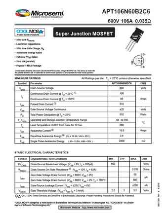
APT106N60B2C6 600V 106A 0.035 COOLMOS Power Semiconductors Super Junction MOSFET Ultra Low RDS(ON) Low Miller Capacitance Ultra Low Gate Charge, Qg Avalanche Energy Rated D Extreme dv/dt Rated Dual die (parallel) G Popular T-MAX Package S Unless stated otherwise, Microsemi discrete MOSFETs contain a single MOSFET die. This device is made with
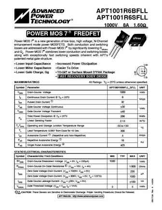
apt10088hvr.pdf
APT10088HVR 1000V 11A 0.880 POWER MOS V TO-258 Power MOS V is a new generation of high voltage N-Channel enhancement mode power MOSFETs. This new technology minimizes the JFET effect, increases packing density and reduces the on-resistance. Power MOS V also achieves faster switching speeds through optimized gate layout. Faster Switching 100% Avalanche Tested D Lowe
apt10m11b2vfrg apt10m11lvfrg.pdf
APT10M11B2VFR APT10M11LVFR 100V 100A 0.011W B2VFR POWER MOS V FREDFET T-MAX Power MOS V is a new generation of high voltage N-Channel enhancement TO-264 mode power MOSFETs. This new technology minimizes the JFET effect, increases packing density and reduces the on-resistance. Power MOS V also achieves faster switching speeds through optimized gate layout. LVFR Identical
apt1004r2bn.pdf
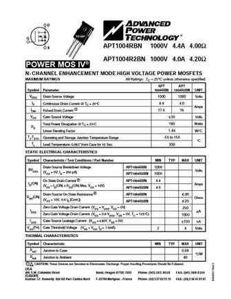
D TO-247 G APT1004RBN 1000V 4.4A 4.00 S APT1004R2BN 1000V 4.0A 4.20 POWER MOS IV N- CHANNEL ENHANCEMENT MODE HIGH VOLTAGE POWER MOSFETS MAXIMUM RATINGS All Ratings TC = 25 C unless otherwise specified. APT APT Symbol Parameter 1004RBN 1004R2BN UNIT VDSS Drain-Source Voltage 1000 1000 Volts ID Continuous Drain Current @ TC = 25 C 4.4 4.0 Amps IDM Pulsed Drain Current 1
apt10026l2ll.pdf
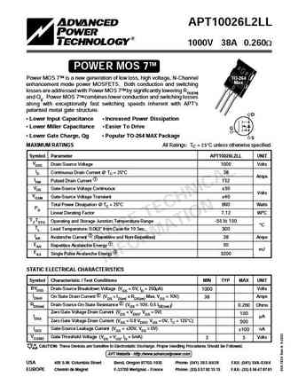
APT10026L2LL 1000V 38A 0.260W TM POWER MOS 7 Power MOS 7TM is a new generation of low loss, high voltage, N-Channel TO-264 Max enhancement mode power MOSFETS. Both conduction and switching losses are addressed with Power MOS 7TM by significantly lowering RDS(ON) and Qg. Power MOS 7TM combines lower conduction and switching losses along with exceptionally fast switching speeds inherent
apt1001r1bn.pdf

D TO-247 G APT1001R1BN 1000V 10.5A 1.10 S APT1001R3BN 1000V 10.0A 1.30 POWER MOS IV N- CHANNEL ENHANCEMENT MODE HIGH VOLTAGE POWER MOSFETS MAXIMUM RATINGS All Ratings TC = 25 C unless otherwise specified. APT APT Symbol Parameter 1001RBN 1001R3BN UNIT VDSS Drain-Source Voltage 1000 1000 Volts ID Continuous Drain Current @ TC = 25 C 10.5 10 Amps IDM Pulsed Drain Curren
apt10m19.pdf

APT10M19BVFR APT10M19SVFR 100V 75A 0.019 BVFR POWER MOS V FREDFET D3PAK Power MOS V is a new generation of high voltage N-Channel enhancement TO-247 mode power MOSFETs. This new technology minimizes the JFET effect, increases packing density and reduces the on-resistance. Power MOS V also achieves faster switching speeds through optimized gate layout. SV
apt10035b2ll.pdf

APT10035B2LL APT10035LLL 1000V 28A 0.350W B2LL TM POWER MOS 7 Power MOS 7TM is a new generation of low loss, high voltage, N-Channel T-MAX TO-264 enhancement mode power MOSFETS. Both conduction and switching losses are addressed with Power MOS 7TM by significantly lowering RDS(ON) and Qg. Power MOS 7TM combines lower conduction and switching losses along with exceptionally fast
apt10m11lvr.pdf

APT10M11LVR 100V 100A 0.011 POWER MOS V Power MOS V is a new generation of high voltage N-Channel enhancement TO-264 mode power MOSFETs. This new technology minimizes the JFET effect, increases packing density and reduces the on-resistance. Power MOS V also achieves faster switching speeds through optimized gate layout.. Faster Switching 100% Avalanche Tested D Low
apt10050b2lc.pdf

APT10050B2LC APT10050LLC 1000V 21A 0.500W B2LC TM POWER MOS VI T-MAX Power MOS VITM is a new generation of low gate charge, high voltage TO-264 N-Channel enhancement mode power MOSFETs. Lower gate charge is achieved by optimizing the manufacturing process to minimize Ciss and Crss. Lower gate charge coupled with Power MOS VITM optimized gate layout, LLC delivers exceptionally fa
apt1003rbllg apt1003rsllg.pdf

APT1003RBLL APT1003RSLL 1000V 4A 3.00 R POWER MOS 7 MOSFET D3PAK TO-247 Power MOS 7 is a new generation of low loss, high voltage, N-Channel enhancement mode power MOSFETS. Both conduction and switching losses are addressed with Power MOS 7 by significantly lowering RDS(ON) and Qg. Power MOS 7 combines lower conduction and switching losses along with exc
apt10025jlc.pdf
APT10025JLC 1000V 34A 0.250W TM POWER MOS VI Power MOS VITM is a new generation of low gate charge, high voltage N-Channel enhancement mode power MOSFETs. Lower gate charge is achieved by optimizing the manufacturing process to minimize Ciss and Crss. Lower gate charge coupled with Power MOS VITM optimized gate layout, "UL Recognized" delivers exceptionally fast switching speeds. ISOT
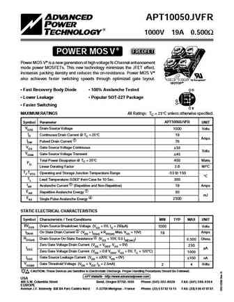
apt10050jvr.pdf

APT10050JVR 1000V 19A 0.500 POWER MOS V Power MOS V is a new generation of high voltage N-Channel enhancement mode power MOSFETs. This new technology minimizes the JFET effect, increases packing density and reduces the on-resistance. Power MOS V also achieves faster switching speeds through optimized gate layout. "UL Recognized" ISOTOP Faster Switching 100% Avalanche
apt10m25svr.pdf
APT10M25SVR 100V 75A 0.025 POWER MOS V D3PAK Power MOS V is a new generation of high voltage N-Channel enhancement mode power MOSFETs. This new technology minimizes the JFET effect, increases packing density and reduces the on-resistance. Power MOS V also achieves faster switching speeds through optimized gate layout. D Faster Switching 100% Avalanche Tested Lower
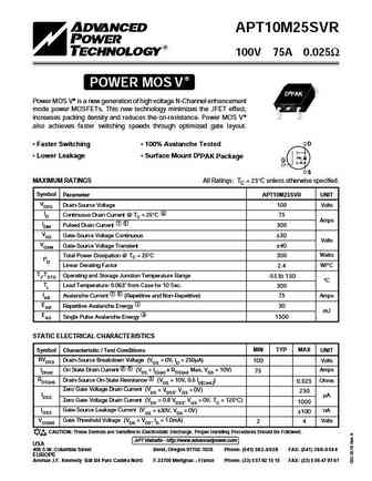
apt10086bvfr.pdf
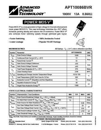
APT10086BVFR 1000V 13A 0.860 POWER MOS V FREDFET Power MOS V is a new generation of high voltage N-Channel enhancement TO-247 mode power MOSFETs. This new technology minimizes the JFET effect, increases packing density and reduces the on-resistance. Power MOS V also achieves faster switching speeds through optimized gate layout. Fast Recovery Body Diode 100% Avalanche Te
apt10045jfll.pdf
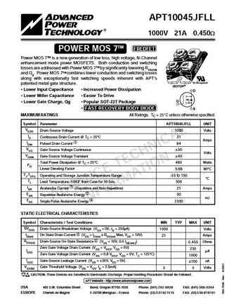
APT10045JFLL 1000V 21A 0.450W TM FREDFET POWER MOS 7 Power MOS 7TM is a new generation of low loss, high voltage, N-Channel enhancement mode power MOSFETS. Both conduction and switching losses are addressed with Power MOS 7TM by significantly lowering RDS(ON) and Qg. Power MOS 7TM combines lower conduction and switching losses along with exceptionally fast switching speeds inherent wi
apt1003rkfllg.pdf
APT1003RKFLL 1000V 4A 3.00 R POWER MOS 7 FREDFET TO-220 Power MOS 7 is a new generation of low loss, high voltage, N-Channel enhancement mode power MOSFETS. Both conduction and switching losses are addressed with Power MOS 7 by significantly lowering RDS(ON) and Qg. Power MOS 7 combines lower conduction and switching losses G D S along with exceptionall
apt10025pvr.pdf
APT10025PVR 1000V 33A 0.250 POWER MOS V P-Pack Power MOS V is a new generation of high voltage N-Channel enhancement mode power MOSFETs. This new technology minimizes the JFET effect, increases packing density and reduces the on-resistance. Power MOS V also achieves faster switching speeds through optimized gate layout. Faster Switching 100% Avalanche Tested D Lowe
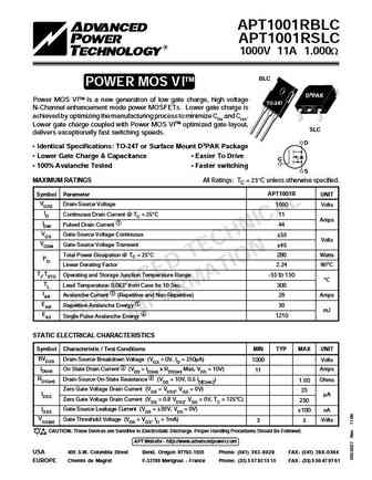
apt1001rsvr.pdf
APT1001RSVR 1000V 11A 1.000 POWER MOS V D3PAK Power MOS V is a new generation of high voltage N-Channel enhancement mode power MOSFETs. This new technology minimizes the JFET effect, increases packing density and reduces the on-resistance. Power MOS V also achieves faster switching speeds through optimized gate layout. D Faster Switching 100% Avalanche Tested Lowe
apt10026l2fll.pdf
APT10026L2FLL 1000V 38A 0.260W TM FREDFET POWER MOS 7 Power MOS 7TM is a new generation of low loss, high voltage, N-Channel TO-264 Max enhancement mode power MOSFETS. Both conduction and switching losses are addressed with Power MOS 7TM by significantly lowering RDS(ON) and Qg. Power MOS 7TM combines lower conduction and switching losses along with exceptionally fast switching speed
apt10050b2vr.pdf
APT10050B2VR 1000V 21A 0.500 POWER MOS V T-MAX Power MOS V is a new generation of high voltage N-Channel enhancement mode power MOSFETs. This new technology minimizes the JFET effect, increases packing density and reduces the on-resistance. Power MOS V also achieves faster switching speeds through optimized gate layout. Faster Switching 100% Avalanche Tested D L
apt1003rkll.pdf
APT1003RKLL 1000V 4A 3.00 R POWER MOS 7 MOSFET TO-220 Power MOS 7 is a new generation of low loss, high voltage, N-Channel enhancement mode power MOSFETS. Both conduction and switching losses are addressed with Power MOS 7 by significantly lowering RDS(ON) G and Qg. Power MOS 7 combines lower conduction and switching losses D S along with exceptionally
apt100gt120ju2.pdf
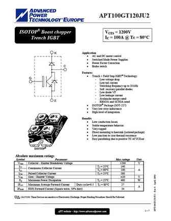
APT100GT120JU2 ISOTOP Boost chopper VCES = 1200V IC = 100A @ Tc = 80 C Trench IGBT Application K AC and DC motor control Switched Mode Power Supplies Power Factor Correction C Brake switch Features Trench + Field Stop IGBT Technology G - Low voltage drop - Low tail current - Switching frequency up to 20 kHz - Soft recovery parallel diodes -
apt10043.pdf
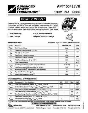
APT10043JVR 1000V 22A 0.430 POWER MOS V Power MOS V is a new generation of high voltage N-Channel enhancement mode power MOSFETs. This new technology minimizes the JFET effect, increases packing density and reduces the on-resistance. Power MOS V also achieves faster switching speeds through optimized gate layout. "UL Recognized" ISOTOP Faster Switching 100% Avalanche
apt10026l2fllg.pdf
APT10026L2FLL 1000V 38A 0.260 R POWER MOS 7 FREDFET TO-264 Power MOS 7 is a new generation of low loss, high voltage, N-Channel Max enhancement mode power MOSFETS. Both conduction and switching losses are addressed with Power MOS 7 by significantly lowering RDS(ON) and Qg. Power MOS 7 combines lower conduction and switching losses along with exceptionally
apt10045b2fll.pdf
APT10045B2FLL APT10045LFLL 1000V 23A 0.450W TM FREDFET POWER MOS 7 B2FLL Power MOS 7TM is a new generation of low loss, high voltage, N-Channel enhancement mode power MOSFETS. Both conduction and switching T-MAX TO-264 losses are addressed with Power MOS 7TM by significantly lowering RDS(ON) and Qg. Power MOS 7TM combines lower conduction and switching losses along with excepti
apt10m25.pdf
APT10M25BVFR 100V 75A 0.025 POWER MOS V FREDFET Power MOS V is a new generation of high voltage N-Channel enhancement TO-247 mode power MOSFETs. This new technology minimizes the JFET effect, increases packing density and reduces the on-resistance. Power MOS V also achieves faster switching speeds through optimized gate layout. Fast Recovery Body Diode 100% Avalanche Tes
apt100gn60ldq4g.pdf
TYPICAL PERFORMANCE CURVES APT100GN60LDQ4(G) 600V APT100GN60LDQ4 APT100GN60LDQ4G* *G Denotes RoHS Compliant, Pb Free Terminal Finish. Utilizing the latest Field Stop and Trench Gate technologies, these IGBT's have ultra low VCE(ON) and are ideal for low frequency applications that require absolute minimum TO-264 conduction loss. Easy paralleling is a result of very tight parame
apt10030l2vfr.pdf
APT10030L2VFR 1000V 33A 0.300W POWER MOS V FREDFET TO-264 Max Power MOS V is a new generation of high voltage N-Channel enhancement mode power MOSFETs. This new technology minimizes the JFET effect, increases packing density and reduces the on-resistance. Power MOS V also achieves faster switching speeds through optimized gate layout. TO-264 MAX Package Faster Switching D
apt100gt120ju3.pdf
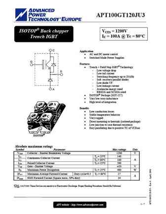
APT100GT120JU3 ISOTOP Buck chopper VCES = 1200V IC = 100A @ Tc = 80 C Trench IGBT C Application AC and DC motor control Switched Mode Power Supplies G Features Trench + Field Stop IGBT Technology - Low voltage drop E - Low tail current - Switching frequency up to 20 kHz - Soft recovery parallel diodes - Low diode VF - Low leakage current - Avalanch
apt10043jvr.pdf

APT10043JVR 1000V 22A 0.430 POWER MOS V Power MOS V is a new generation of high voltage N-Channel enhancement mode power MOSFETs. This new technology minimizes the JFET effect, increases packing density and reduces the on-resistance. Power MOS V also achieves faster switching speeds through optimized gate layout. "UL Recognized" ISOTOP Faster Switching 100% Avalanche
apt1001rslc.pdf
APT1001RBLC APT1001RSLC 1000V 11A 1.000W BLC TM POWER MOS VI D3PAK Power MOS VITM is a new generation of low gate charge, high voltage TO-247 N-Channel enhancement mode power MOSFETs. Lower gate charge is achieved by optimizing the manufacturing process to minimize Ciss and Crss. Lower gate charge coupled with Power MOS VITM optimized gate layout, SLC delivers exceptionally fast sw
apt10m25bvfr.pdf

APT10M25BVFR 100V 75A 0.025 POWER MOS V FREDFET Power MOS V is a new generation of high voltage N-Channel enhancement TO-247 mode power MOSFETs. This new technology minimizes the JFET effect, increases packing density and reduces the on-resistance. Power MOS V also achieves faster switching speeds through optimized gate layout. Fast Recovery Body Diode 100% Avalanche Tes
apt1001rsvfr.pdf
APT1001RBVFR APT1001RSVFR 1000V 11A 1.00 BVFR POWER MOS V FREDFET D3PAK TO-247 Power MOS V is a new generation of high voltage N-Channel enhancement mode power MOSFETs. This new technology minimizes the JFET effect, increases packing density and reduces the on-resistance. Power MOS V SVFR also achieves faster switching speeds through optimized gate layou
apt10050lvr.pdf
APT10050LVR 1000V 21A 0.500 POWER MOS V Power MOS V is a new generation of high voltage N-Channel enhancement TO-264 mode power MOSFETs. This new technology minimizes the JFET effect, increases packing density and reduces the on-resistance. Power MOS V also achieves faster switching speeds through optimized gate layout. Faster Switching 100% Avalanche Tested D Lowe
apt1003rbll.pdf

APT1003RBLL APT1003RSLL 1000V 4A 3.00 R POWER MOS 7 MOSFET D3PAK TO-247 Power MOS 7 is a new generation of low loss, high voltage, N-Channel enhancement mode power MOSFETS. Both conduction and switching losses are addressed with Power MOS 7 by significantly lowering RDS(ON) and Qg. Power MOS 7 combines lower conduction and switching losses along with exc
apt10086blc.pdf

APT10086BLC APT10086SLC 1000V 13A 0.860W BLC TM POWER MOS VI D3PAK Power MOS VITM is a new generation of low gate charge, high voltage TO-247 N-Channel enhancement mode power MOSFETs. Lower gate charge is achieved by optimizing the manufacturing process to minimize Ciss and Crss. Lower gate charge coupled with Power MOS VITM optimized gate layout, SLC delivers exceptionally fast sw
apt10026jll.pdf
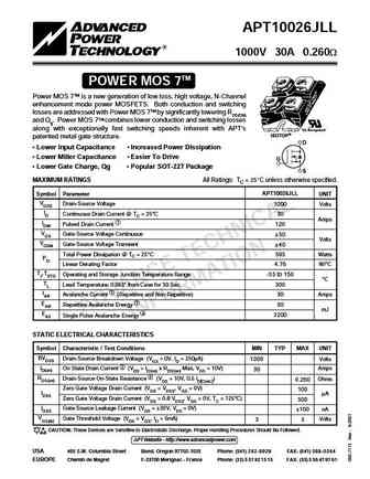
APT10026JLL 1000V 30A 0.260W TM POWER MOS 7 Power MOS 7TM is a new generation of low loss, high voltage, N-Channel enhancement mode power MOSFETS. Both conduction and switching losses are addressed with Power MOS 7TM by significantly lowering RDS(ON) and Qg. Power MOS 7TM combines lower conduction and switching losses along with exceptionally fast switching speeds inherent with APT's
apt10086svr.pdf
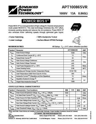
APT10086SVR 1000V 13A 0.860 POWER MOS V Power MOS V is a new generation of high voltage N-Channel enhancement D3PAK mode power MOSFETs. This new technology minimizes the JFET effect, increases packing density and reduces the on-resistance. Power MOS V also achieves faster switching speeds through optimized gate layout. D Faster Switching 100% Avalanche Tested Lower
apt10m11jvfr.pdf
APT10M11JVFR 100V 144A 0.011 POWER MOS V Power MOS V is a new generation of high voltage N-Channel enhancement mode power MOSFETs. This new technology minimizes the JFET effect, increases packing density and reduces the on-resistance. Power MOS V also achieves faster switching speeds through optimized gate layout. "UL Recognized" ISOTOP Faster Switchi
apt10050b2 lvfr c.pdf

APT10050B2VFR APT10050LVFR 1000V 21A 0.500 B2VFR POWER MOS V T-MAX Power MOS V is a new generation of high voltage N-Channel enhancement TO-264 mode power MOSFETs. This new technology minimizes the JFET effect, increases packing density and reduces the on-resistance. Power MOS V also achieves faster switching speeds through optimized gate layout. LVFR
apt1003rkllg.pdf

APT1003RKLL 1000V 4A 3.00 R POWER MOS 7 MOSFET TO-220 Power MOS 7 is a new generation of low loss, high voltage, N-Channel enhancement mode power MOSFETS. Both conduction and switching losses are addressed with Power MOS 7 by significantly lowering RDS(ON) G and Qg. Power MOS 7 combines lower conduction and switching losses D S along with exceptionally
apt10026l2fl.pdf

APT10026L2FLL 1000V 38A 0.260W TM FREDFET POWER MOS 7 Power MOS 7TM is a new generation of low loss, high voltage, N-Channel TO-264 Max enhancement mode power MOSFETS. Both conduction and switching losses are addressed with Power MOS 7TM by significantly lowering RDS(ON) and Qg. Power MOS 7TM combines lower conduction and switching losses along with exceptionally fast switching speed
apt10078bfllg apt10078sfllg.pdf
APT10078BFLL APT10078SFLL 1000V 14A 0.780 BFLL R FREDFET POWER MOS 7 FREDFET D3PAK Power MOS 7 is a new generation of low loss, high voltage, N-Channel TO-247 enhancement mode power MOSFETS. Both conduction and switching losses are addressed with Power MOS 7 by significantly lowering RDS(ON) and Qg. Power MOS 7 combines lower conduction and switching los
apt10035b2fllg apt10035lfllg.pdf
APT10035B2FLL(G) APT10035LFLL(G) 1000V 28A 0.37 R B2FLL POWER MOS 7 FREDFET Power MOS 7 is a new generation of low loss, high voltage, N-Channel T-MAX TO-264 enhancement mode power MOSFETS. Both conduction and switching losses are addressed with Power MOS 7 by significantly lowering RDS(ON) and Qg. Power MOS 7 combines lower conduction and switching
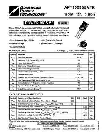
apt10086bvr.pdf
APT10086BVR 1000V 13A 0.860 POWER MOS V Power MOS V is a new generation of high voltage N-Channel enhancement TO-247 mode power MOSFETs. This new technology minimizes the JFET effect, increases packing density and reduces the on-resistance. Power MOS V also achieves faster switching speeds through optimized gate layout. Faster Switching 100% Avalanche Tested D Lower
apt10040lvr.pdf

APT10040B2VR APT10040LVR 1000V 25A 0.400W B2VR POWER MOS V T-MAX Power MOS V is a new generation of high voltage N-Channel enhancement TO-264 mode power MOSFETs. This new technology minimizes the JFET effect, increases packing density and reduces the on-resistance. Power MOS V also achieves faster switching speeds through optimized gate layout. LVR Identical Specificati
apt1004r2kn.pdf
D TO-220 G APT1004RKN 1000V 3.6A 4.00 S APT1004R2KN 1000V 3.5A 4.20 POWER MOS IV N- CHANNEL ENHANCEMENT MODE HIGH VOLTAGE POWER MOSFETS MAXIMUM RATINGS All Ratings TC = 25 C unless otherwise specified. Symbol Parameter APT1004R2KN APT1004RKN UNIT VDSS Drain-Source Voltage 1000 1000 Volts ID Continuous Drain Current 3.5 3.6 Amps 1 IDM Pulsed Drain Current 14.0 14.4 Amps
apt1004rkn.pdf
D TO-220 G APT1004RKN 1000V 3.6A 4.00 S APT1004R2KN 1000V 3.5A 4.20 POWER MOS IV N- CHANNEL ENHANCEMENT MODE HIGH VOLTAGE POWER MOSFETS MAXIMUM RATINGS All Ratings TC = 25 C unless otherwise specified. Symbol Parameter APT1004R2KN APT1004RKN UNIT VDSS Drain-Source Voltage 1000 1000 Volts ID Continuous Drain Current 3.5 3.6 Amps 1 IDM Pulsed Drain Current 14.0 14.4 Amps V
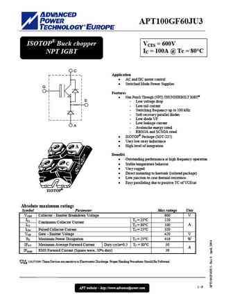
apt100gf60ju2.pdf

APT100GF60JU2 ISOTOP Boost chopper VCES = 600V IC = 100A @ Tc = 80 C NPT IGBT Application AC and DC motor control K Switched Mode Power Supplies Power Factor Correction Brake switch C Features Non Punch Through (NPT) THUNDERBOLT IGBT G - Low voltage drop - Low tail current - Switching frequency up to 100 kHz - Soft recovery parallel diodes -
apt10m19bvfrg apt10m19svfr apt10m19svfrg.pdf
APT10M19BVFR APT10M19SVFR 100V 75A 0.019 BVFR POWER MOS V FREDFET D3PAK Power MOS V is a new generation of high voltage N-Channel enhancement TO-247 mode power MOSFETs. This new technology minimizes the JFET effect, increases packing density and reduces the on-resistance. Power MOS V also achieves faster switching speeds through optimized gate layout. SV
apt1001rbn.pdf
D TO-247 G APT1001RBN 1000V 11.0A 1.00 S APT5030BN 500V 21.0A 0.30 POWER MOS IV N- CHANNEL ENHANCEMENT MODE HIGH VOLTAGE POWER MOSFETS MAXIMUM RATINGS All Ratings TC = 25 C unless otherwise specified. APT Symbol Parameter 1001RBN UNIT VDSS Drain-Source Voltage 1000 Volts ID Continuous Drain Current @ TC = 25 C 11 Amps IDM Pulsed Drain Current 1 44 VGS Gate-Source Vo
apt10030l2vfrg.pdf
APT10030L2VFR 1000V 33A 0.300 POWER MOS V FREDFET TO-264 Max Power MOS V is a new generation of high voltage N-Channel enhancement mode power MOSFETs. This new technology minimizes the JFET effect, increases packing density and reduces the on-resistance. Power MOS V also achieves faster switching speeds through optimized gate layout. D TO-264 MAX Pack
apt10050b2vfrg apt10050lvfrg.pdf
APT10050B2VFR APT10050LVFR 1000V 21A 0.500 B2VFR POWER MOS V T-MAX Power MOS V is a new generation of high voltage N-Channel enhancement TO-264 mode power MOSFETs. This new technology minimizes the JFET effect, increases packing density and reduces the on-resistance. Power MOS V also achieves faster switching speeds through optimized gate layout. LVFR
apt100gf60jrd.pdf
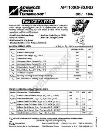
APT100GF60JRD 600V 140A Fast IGBT & FRED The Fast IGBT is a new generation of high voltage power IGBTs. Using Non- Punch Through Technology the Fast IGBT combined with an APT free- wheeling ultraFast Recovery Epitaxial Diode (FRED) offers superior ruggedness and fast switching speed. "UL Recognized" ISOTOP Low Forward Voltage Drop High Freq. Switching to 20KHz C L
apt10026jn.pdf
D G APT10026JN 1000V 33A 0.26 S "UL Recognized" File No. E145592 (S) ISOTOP POWER MOS IV SINGLE DIE ISOTOP PACKAGE N- CHANNEL ENHANCEMENT MODE HIGH VOLTAGE POWER MOSFETS MAXIMUM RATINGS All Ratings TC = 25 C unless otherwise specified. APT Symbol Parameter 10026JN UNIT VDSS Drain-Source Voltage 1000 Volts ID Continuous Drain Current @ TC = 25 C 33 Amps IDM, lLM Pulse
apt100m50j.pdf
APT100M50J 500V, 103A, 0.036 Max N-Channel MOSFET Power MOS 8 is a high speed, high voltage N-channel switch-mode power MOSFET. A proprietary planar stripe design yields excellent reliability and manufacturability. Low switching loss is achieved with low input capacitance and ultra low Crss "Miller" capaci- tance. The intrinsic gate resistance and capacitance of the poly-silicon
apt1002r4bn.pdf

D TO-247 G APT1002RBN 1000V 7.0A 2.00 S APT1002R4BN 1000V 6.5A 2.40 POWER MOS IV N- CHANNEL ENHANCEMENT MODE HIGH VOLTAGE POWER MOSFETS MAXIMUM RATINGS All Ratings TC = 25 C unless otherwise specified. APT APT Symbol Parameter 1002RBN 1002R4BN UNIT VDSS Drain-Source Voltage 1000 1000 Volts ID Continuous Drain Current @ TC = 25 C 7.0 6.5 Amps IDM Pulsed Drain Current 1
apt10026jfll.pdf

APT10026JFLL 1000V 30A 0.140W TM FREDFET POWER MOS 7 Power MOS 7TM is a new generation of low loss, high voltage, N-Channel enhancement mode power MOSFETS. Both conduction and switching losses are addressed with Power MOS 7TM by significantly lowering RDS(ON) and Qg. Power MOS 7TM combines lower conduction and switching losses along with exceptionally fast switching speeds inherent wi
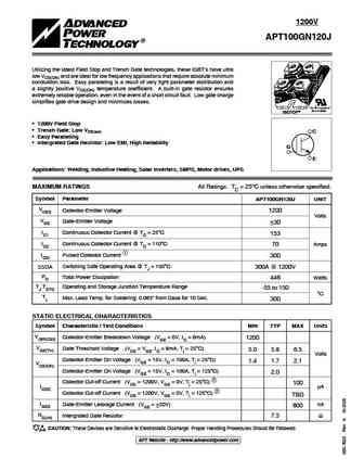
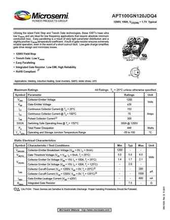
apt100gn120jdq4.pdf
APT100GN120JDQ4 1200V, 100A, VCE(ON) = 1.7V Typical Utilizing the latest Field Stop and Trench Gate technologies, these IGBT s have ultra low V and are ideal for low frequency applications that require absolute minimum CE(ON) conduction loss. Easy paralleling is a result of very tight parameter distribution and a slightly positive V temperature coefficient. A built-in gate resistor
apt100gt120jrdl.pdf
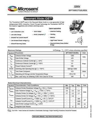
1200V APT100GT120JRDL Resonant Mode IGBT The Thunderbolt IGBT used in this Resonant Mode Combi is a new generation of high voltage power IGBTs. Using Non- Punch Through Technology, the Thunderblot IGBT of- fers superior ruggedness and ultrafast switching speed. Typical Applications Features Induction Heating SSOA Rated Low Conduction Loss "UL Recognized" ISOT
apt100gt60jr.pdf
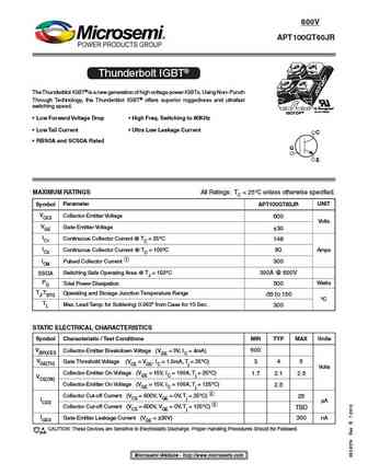
TYPICAL PERFORMANCE CURVES APT100GT60JR 600V APT100GT60JR Thunderbolt IGBT The Thunderblot IGBT is a new generation of high voltage power IGBTs. Using Non- Punch Through Technology, the Thunderblot IGBT offers superior ruggedness and ultrafast switching speed. "UL Recognized" ISOTOP file # E145592 Low Forward Voltage Drop High Freq. Switching to 80KHz Low Tail C
apt100gt120jr.pdf
APT100GT120JR 1200V, 100A, VCE(ON) = 3.2V Typical Thunderbolt IGBT The Thunderbolt IGBT is a new generation of high voltage power IGBTs. Using Non- Punch-Through Technology, the Thunderbolt IGBT offers superior ruggedness and ultrafast switching speed. Features RBSOA and SCSOA Rated Low Forward Voltage Drop "UL Recognized" High Frequency Switching to 50KHz L
apt100gn60b2g.pdf
APT100GT60B2R(G) APT100GT60LR(G) 600V, 100A, VCE(ON) = 2.1V Typical Thunderbolt IGBT The Thunderbolt IGBT is a new generation of high voltage power IGBTs. Using Non-Punch-Through Technology, the Thunderbolt IGBT offers superior rugged- ness and ultrafast switching speed. Features RBSOA and SCSOA Rated G Low Forward Voltage Drop CE G CE High Frequency Switching t
apt100gt60jrdl.pdf
APT100GT60JRDL 600V, 100A, VCE(ON) = 2.1V Typical Resonant Mode Combi IGBT The Thunderbolt IGBT used in this Resonant Mode Combi is a new generation of high voltage power IGBTs. Using Non-Punch-Through Technology, the Thun- derbolt IGBT offers superior ruggedness and ultrafast switching speed. Typical Applications "UL Recognized" Features ISOTOP file # E145592 Ultra soft
apt100gn120b2g.pdf
TYPICAL PERFORMANCE CURVES APT100GN120B2 1200V APT100GN120B2 APT100GN120B2G* *G Denotes RoHS Compliant, Pb Free Terminal Finish. Utilizing the latest Field Stop and Trench Gate technologies, these IGBT's have ultra low VCE(ON) and are ideal for low frequency applications that require absolute minimum T-Max conduction loss. Easy paralleling is a result of very tight parameter d
apt100gt60jrdq4.pdf
APT100GT60JRDQ4 600V, 100A, VCE(ON) = 2.1V Typical Thunderbolt IGBT The Thunderbolt IGBT is a new generation of high voltage power IGBTs. Using Non-Punch-Through Technology, the Thunderbolt IGBT offers superior rugged- ness and ultrafast switching speed. Features RBSOA and SCSOA Rated Low Forward Voltage Drop "UL Recognized" High Frequency Switching to 50KHz
apt10m19bvr.pdf
isc N-Channel MOSFET Transistor APT10M19BVR FEATURES Drain Current I =75A@ T =25 D C Drain Source Voltage- V =100V(Min) DSS Static Drain-Source On-Resistance R =0.019 (Max) DS(on) 100% avalanche tested Minimum Lot-to-Lot variations for robust device performance and reliable operation DESCRIPTION Designed for use in switch mode power supplies and general pur
apt10m09lvfr.pdf
isc N-Channel MOSFET Transistor APT10M09LVFR FEATURES Drain Current I = 100A@ T =25 D C Drain Source Voltage- V =100V(Min) DSS Static Drain-Source On-Resistance R =0.009 (Max) DS(on) 100% avalanche tested Minimum Lot-to-Lot variations for robust device performance and reliable operation DESCRIPTION Designed for use in switch mode power supplies and general
apt10m09b2vfr.pdf

isc N-Channel MOSFET Transistor APT10M09B2VFR FEATURES Drain Current I = 100A@ T =25 D C Drain Source Voltage- V =100V(Min) DSS Static Drain-Source On-Resistance R =0.009 (Max) DS(on) 100% avalanche tested Minimum Lot-to-Lot variations for robust device performance and reliable operation DESCRIPTION Designed for use in switch mode power supplies and general
apt10m25bvr.pdf

isc N-Channel MOSFET Transistor APT10M25BVR FEATURES Drain Current I =75A@ T =25 D C Drain Source Voltage- V =100V(Min) DSS Static Drain-Source On-Resistance R =0.025 (Max) DS(on) 100% avalanche tested Minimum Lot-to-Lot variations for robust device performance and reliable operation DESCRIPTION Designed for use in switch mode power supplies and general pur
Otros transistores... APT75GP120B2G , APT100GN120B2G , MPMC200B120RH , F3L300R07PE4 , APT65GP60L2DQ2G , MPMD150B120RH , IXYT80N90C3 , APT102GA60B2 , SGT60N60FD1P7 , MPMD100B120RH , IRGPS4067D , MPMC150B120RH , MPMC100B120RH , APT200GN60B2G , TGL40N120FD , TGL40N120ND , IGW75N60H3 .
🌐 : EN ES РУ

Liste
Recientemente añadidas las descripciónes de los transistores
IGBT: JJT40N120SE | JJT40N120HE | JJT30N65UE | JJT30N65SY | JJT30N65SS | JJT30N65SE | JJT40N65UH | JJT40N65UE | JJT40N65LE | JJT40N65HE | JJT40N135UE
Popular searches
2sd315 | a1013 | 2sb554 | 2sd2560 | 2sc2078 transistor | bc558 datasheet | p75nf75 mosfet | ao4407a