APT5020SVFR MOSFET Equivalente. Reemplazo. Hoja de especificaciones. Principales características
Número de Parte: APT5020SVFR
Tipo de FET: MOSFET
Polaridad de transistor: N
ESPECIFICACIONES MÁXIMAS
Pdⓘ - Máxima disipación de potencia: 300 W
|Vds|ⓘ - Voltaje máximo drenador-fuente: 500 V
|Vgs|ⓘ - Voltaje máximo fuente-puerta: 30 V
|Id|ⓘ - Corriente continua de drenaje: 26 A
Tjⓘ - Temperatura máxima de unión: 150 °C
CARACTERÍSTICAS ELÉCTRICAS
trⓘ - Tiempo de subida: 10 nS
Cossⓘ - Capacitancia de salida: 510 pF
RDSonⓘ - Resistencia estado encendido drenaje a fuente: 0.2 Ohm
Encapsulados: D3PAK
Búsqueda de reemplazo de APT5020SVFR MOSFET
- Selecciónⓘ de transistores por parámetros
APT5020SVFR datasheet
apt5020svfr.pdf
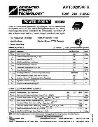
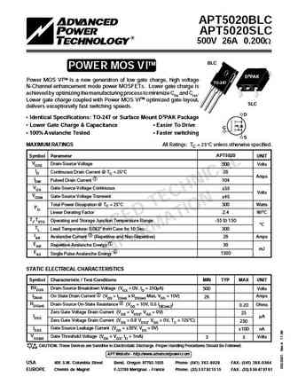
APT5020SVFR 500V 26A 0.200 POWER MOS V FREDFET D3PAK Power MOS V is a new generation of high voltage N-Channel enhancement mode power MOSFETs. This new technology minimizes the JFET effect, increases packing density and reduces the on-resistance. Power MOS V also achieves faster switching speeds through optimized gate layout. Fast Recovery Body Diode 100% Avalanche Test
apt5020svr.pdf
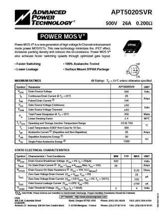
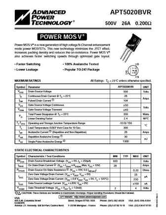
APT5020SVR 500V 26A 0.200 POWER MOS V Power MOS V is a new generation of high voltage N-Channel enhancement D3PAK mode power MOSFETs. This new technology minimizes the JFET effect, increases packing density and reduces the on-resistance. Power MOS V also achieves faster switching speeds through optimized gate layout. Faster Switching 100% Avalanche Tested D Lower Le
apt5020bn.pdf
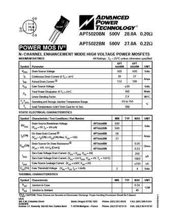
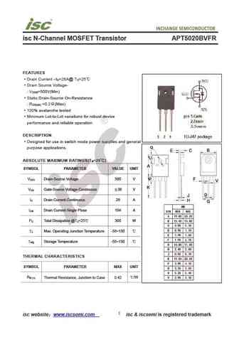
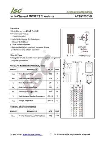
D TO-247 G APT5020BN 500V 28.0A 0.20 S APT5022BN 500V 27.0A 0.22 POWER MOS IV N- CHANNEL ENHANCEMENT MODE HIGH VOLTAGE POWER MOSFETS MAXIMUM RATINGS All Ratings TC = 25 C unless otherwise specified. APT APT Symbol Parameter 5020BN 5022BN UNIT VDSS Drain-Source Voltage 500 500 Volts ID Continuous Drain Current @ TC = 25 C 28 27 Amps IDM Pulsed Drain Current 1 112 108
apt5020bvfr.pdf
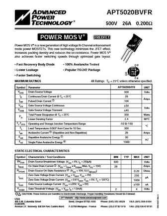
APT5020BVFR 500V 26A 0.200 POWER MOS V FREDFET Power MOS V is a new generation of high voltage N-Channel enhancement TO-247 mode power MOSFETs. This new technology minimizes the JFET effect, increases packing density and reduces the on-resistance. Power MOS V also achieves faster switching speeds through optimized gate layout. Fast Recovery Body Diode 100% Avalanche Test

Otros transistores... APT5015BVR, APT5017BVFR, APT5017BVR, APT5017SVR, APT5019HVR, APT5020BN, APT5020BVFR, APT5020BVR, CS150N03A8, APT5020SVR, APT5022AVR, APT5024AVR, APT5024BVFR, APT5024BVR, APT5025BN, APT5026HVR, APT5028BVR
🌐 : EN ES РУ

Liste
Recientemente añadidas las descripciónes de los transistores:
MOSFET: AUW033N08BG | AUW025N10 | AUR030N10 | AUR020N10 | AUR020N085 | AUR014N10 | AUP074N10 | AUP065N10 | AUP062N08BG | AUP060N08AG | HYG053N10NS1B | HYG053N10NS1P | AP220N04T | AP220N04P | QM3126M3 | AUP060N055
Popular searches
2sc536 | d718 transistor | irfp250n datasheet | 2n5550 | 2sd1047 | 2n3035 | ksc1815 | bu406