IPB60R950C6 MOSFET Equivalente. Reemplazo. Hoja de especificaciones. Principales características
Número de Parte: IPB60R950C6
Tipo de FET: MOSFET
Polaridad de transistor: N
ESPECIFICACIONES MÁXIMAS
Pdⓘ - Máxima disipación de potencia: 37 W
|Vds|ⓘ - Voltaje máximo drenador-fuente: 600 V
|Vgs|ⓘ - Voltaje máximo fuente-puerta: 20 V
|Id|ⓘ - Corriente continua de drenaje: 4.4 A
Tjⓘ - Temperatura máxima de unión: 150 °C
CARACTERÍSTICAS ELÉCTRICAS
trⓘ - Tiempo de subida: 8 nS
Cossⓘ - Capacitancia de salida: 21 pF
RDSonⓘ - Resistencia estado encendido drenaje a fuente: 0.95 Ohm
Encapsulados: TO263
Búsqueda de reemplazo de IPB60R950C6 MOSFET
- Selecciónⓘ de transistores por parámetros
IPB60R950C6 datasheet
ipb60r950c6.pdf
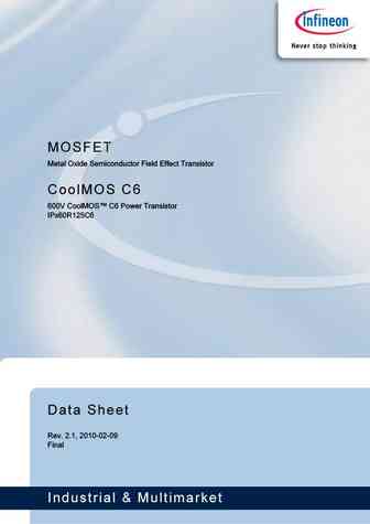
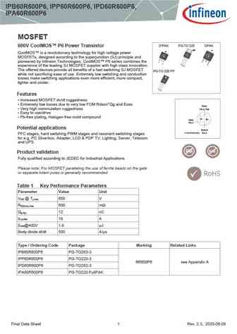
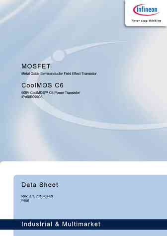
MOSFET Metal Oxide Semiconductor Field Effect Transistor CoolMOS C6 600V CoolMOS C6 Power Transistor IPx60R950C6 Data Sheet Rev. 2.1, 2010-03-11 Final Industrial & Multimarket 600V CoolMOS C6 Power Transistor IPD60R950C6, IPB60R950C6 IPP60R950C6, IPA60R950C6 1 Description CoolMOS is a revolutionary technology for high voltage power MOSFETs, designed according to the supe
ipd60r950c6 ipb60r950c6 ipp60r950c6 ipa60r950c6.pdf

MOSFET Metal Oxide Semiconductor Field Effect Transistor CoolMOS C6 600V 600V CoolMOS C6 Power Transistor IPx60R950C6 Data Sheet Rev. 2.4 Final Power Management & Multimarket 600V CoolMOS C6 Power Transistor IPD60R950C6, IPB60R950C6 IPP60R950C6, IPA60R950C6 1 Description CoolMOS is a revolutionary technology for high voltage power MOSFETs, designed according to the sup
ipb60r950c6.pdf

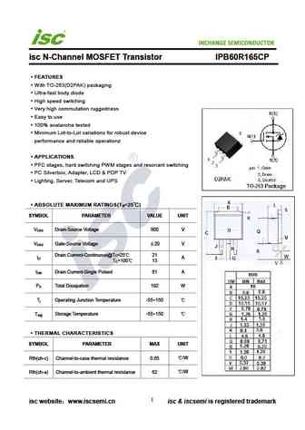
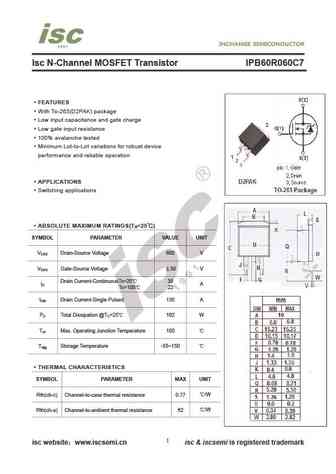
Isc N-Channel MOSFET Transistor IPB60R950C6 FEATURES With To-263(D2PAK) package Low input capacitance and gate charge Low gate input resistance 100% avalanche tested Minimum Lot-to-Lot variations for robust device performance and reliable operation APPLICATIONS Switching applications ABSOLUTE MAXIMUM RATINGS(T =25 ) a SYMBOL PARAMETER VALUE UNIT V Drain-Source V
ipa60r160c6 ipb60r160c6 ipp60r160c6 ipw60r160c6.pdf

MOSFET Metal Oxide Semiconductor Field Effect Transistor CoolMOS C6 600V 600V CoolMOS C6 Power Transistor IPx60R160C6 Data Sheet Rev. 2.3 Final Power Management & Multimarket 600V CoolMOS C6 Power Transistor IPA60R160C6, IPB60R160C6 IPP60R160C6 IPW60R160C6 1 Description CoolMOS is a revolutionary technology for high voltage power MOSFETs, designed according to the superjunct
ipb60r199cpa.pdf
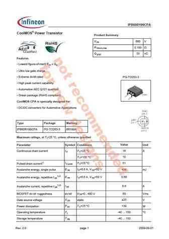
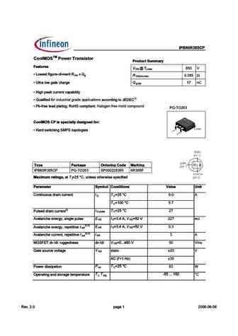
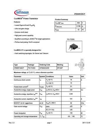
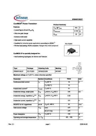
IPB60R199CPA CoolMOS Power Transistor Product Summary V 600 V DS R 0.199 DS(on),max Q 33 nC g,typ Features Lowest figure-of-merit Ron x Qg Ultra low gate charge Extreme dv/dt rated PG-TO263-3 High peak current capability Automotive AEC Q101 qualified Green package (RoHS compliant) CoolMOS CPA is specially designed for DC/DC converters for Auto
ipb60r045p7.pdf
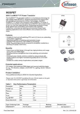
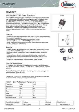
IPB60R045P7 MOSFET D PAK 600V CoolMOS P7 Power Transistor The CoolMOS 7th generation platform is a revolutionary technology for tab high voltage power MOSFETs, designed according to the superjunction (SJ) principle and pioneered by Infineon Technologies. The 600V CoolMOS P7 series is the successor to the CoolMOS P6 series. It combines the benefits of a fast switching SJ MOS
ipd60r600c6 ipb60r600c6 ipp60r600c6 ipa60r600c6.pdf

MOSFET Metal Oxide Semiconductor Field Effect Transistor CoolMOS C6 600V 600V CoolMOS C6 Power Transistor IPx60R600C6 Data Sheet Rev. 2.5 Final Power Management & Multimarket 600V C IMOS C6 P wer Transist r IPD60R600C6, IPB60R600C6 IPP60R600C6, IPA60R600C6 1 Descripti n CoolMOS is a revolutionary technology for high voltage power MOSFETs designed according to the super
ipb60r070cfd7.pdf

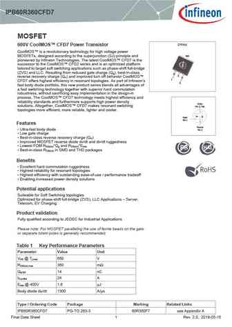
IPB60R070CFD7 MOSFET D PAK 600V CoolMOS CFD7 Power Transistor CoolMOS is a revolutionary technology for high voltage power tab MOSFETs, designed according to the superjunction (SJ) principle and pioneered by Infineon Technologies. The latest CoolMOS CFD7 is the successor to the CoolMOS CFD2 series and is an optimized platform tailored to target soft switching applications s
ipb60r099p7.pdf

IPB60R099P7 MOSFET D PAK 600V CoolMOS P7 Power Transistor The CoolMOS 7th generation platform is a revolutionary technology for tab high voltage power MOSFETs, designed according to the superjunction (SJ) principle and pioneered by Infineon Technologies. The 600V CoolMOS P7 series is the successor to the CoolMOS P6 series. It combines the benefits of a fast switching SJ MOS
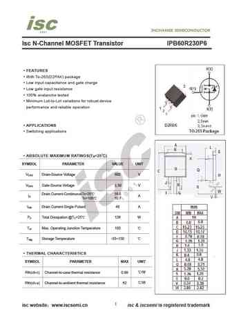
ipb60r230p6 ipw60r230p6 ipb60r230p6 ipp60r230p6 ipa60r230p6.pdf

MOSFET Metal Oxide Semiconductor Field Effect Transistor CoolMOS P6 600V CoolMOS P6 Power Transistor IPx60R230P6 Data Sheet Rev. 2.2 Final Power Management & Multimarket 600V CoolMOS P6 Power Transistor IPW60R230P6, IPB60R230P6, IPP60R230P6, IPA60R230P6 TO-247 D PAK TO-220 1 Description tab tab CoolMOS is a revolutionary technology for high voltage power MOSFETs,
ipb60r099cpa.pdf
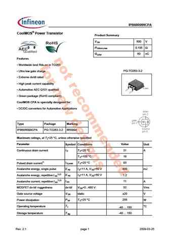
IPB60R099CPA CoolMOS Power Transistor Product Summary V 600 V DS R 0.105 DS(on),max Q 60 nC g,typ Features Worldwide best Rds,on in TO263 PG-TO263-3-2 Ultra low gate charge Extreme dv/dt rated High peak current capability Automotive AEC Q101 qualified Green package (RoHS compliant) CoolMOS CPA is specially designed for DC/DC converters for A
ipb60r299cp.pdf
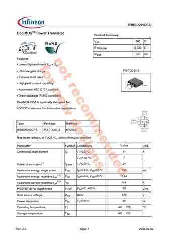
IPB60R299CP C IMOSTM # A0 9 for industrial grade applications 688DG9>CC6CI; Halogen free mold compound 7!"%
ipb60r120c7.pdf

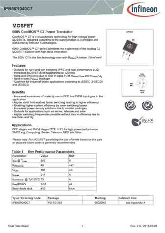
MOSFET Metal Oxide Semiconductor Field Effect Transistor CoolMOS C7 600V CoolMOS C7 Power Transistor IPB60R120C7 Data Sheet Rev. 2.0 Final Power Management & Multimarket 600V CoolMOS C7 Power Transistor IPB60R120C7 D PAK 1 Description CoolMOS C7 is a revolutionary technology for high voltage power MOSFETs, designed according to the superjunction (SJ) principle and ta
ipb60r160c6.pdf

MOSFET Metal Oxide Semiconductor Field Effect Transistor CoolMOS C6 600V CoolMOS C6 Power Transistor IPx60R160C6 Data Sheet Rev. 2.1, 2010-02-09 Final Industrial & Multimarket 600V CoolMOS C6 Power Transistor IPA60R160C6, IPB60R160C6 IPP60R160C6 IPW60R160C6 1 Description CoolMOS is a revolutionary technology for high voltage power MOSFETs, designed according to the superj
ipb60r165cp.pdf
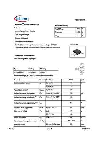
IPB60R165CP CoolMOS Power Transistor Product Summary Features V @ Tj,max 650 V DS Lowest figure-of-merit RONxQg R 0.165 DS(on),max Ultra low gate charge Q 39 nC g,typ Extreme dv/dt rated High peak current capability Qualified according to JEDEC1) for target applications PG-TO263 Pb-free lead plating; RoHS compliant CoolMOS CP is specially designed
ipb60r170cfd7.pdf
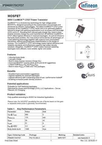
IPB60R170CFD7 MOSFET D PAK 600V CoolMOS CFD7 Power Transistor CoolMOS is a revolutionary technology for high voltage power tab MOSFETs, designed according to the superjunction (SJ) principle and pioneered by Infineon Technologies. The latest CoolMOS CFD7 is the successor to the CoolMOS CFD2 series and is an optimized platform tailored to target soft switching applications s
ipw60r330p6 ipb60r330p6 ipp60r330p6 ipa60r330p6.pdf

MOSFET Metal Oxide Semiconductor Field Effect Transistor CoolMOS P6 600V CoolMOS P6 Power Transistor IPx60R330P6 Data Sheet Rev. 2.2 Final Power Management & Multimarket 600V CoolMOS P6 Power Transistor IPW60R330P6, IPB60R330P6, IPP60R330P6, IPA60R330P6 TO-247 D PAK TO-220 1 Description tab tab CoolMOS is a revolutionary technology for high voltage power MOSFETs,
ipb60r250cp.pdf
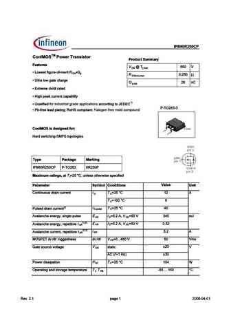
IPB60R250CP C IMOSTM # A0 9 for industrial grade applications 688DF9>CC6CH; Halogen free mold compound 7!
ipb60r099c7.pdf

IPB60R099C7 MOSFET D PAK 600V CoolMOS C7 Power Transistor CoolMOS C7 is a revolutionary technology for high voltage power tab MOSFETs, designed according to the superjunction (SJ) principle and pioneered by Infineon Technologies. 600V CoolMOS C7 series combines the experience of the leading SJ MOSFET supplier with high class innovation. 2 1 The 600V C7 is the first technolo
ipb60r210cfd7.pdf

IPB60R210CFD7 MOSFET D PAK 600V CoolMOS CFD7 Power Transistor CoolMOS is a revolutionary technology for high voltage power tab MOSFETs, designed according to the superjunction (SJ) principle and pioneered by Infineon Technologies. The latest CoolMOS CFD7 is the successor to the CoolMOS CFD2 series and is an optimized platform tailored to target soft switching applications s
ipb60r180p7.pdf
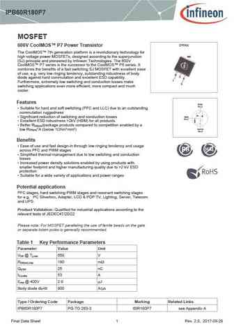
IPB60R180P7 MOSFET D PAK 600V CoolMOS P7 Power Transistor The CoolMOS 7th generation platform is a revolutionary technology for tab high voltage power MOSFETs, designed according to the superjunction (SJ) principle and pioneered by Infineon Technologies. The 600V CoolMOS P7 series is the successor to the CoolMOS P6 series. It combines the benefits of a fast switching SJ MOS
ipb60r125cp.pdf
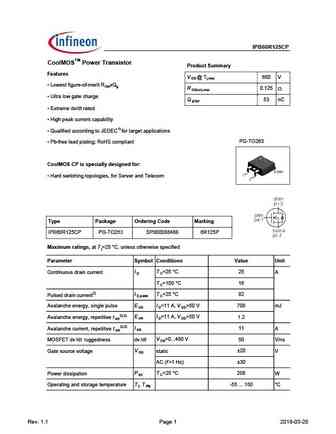
IPB60R125CP CoolMOSTM Power Transistor Product Summary Features V @ Tj,max 650 V DS Lowest figure-of-merit RONxQg R 0.125 DS(on),max Ultra low gate charge Q 53 nC g,typ Extreme dv/dt rated High peak current capability Qualified according to JEDEC1) for target applications PG-TO263 Pb-free lead plating; RoHS compliant CoolMOS CP is specially designe
ipw60r160p6 ipb60r160p6 ipp60r160p6 ipa60r160p6.pdf

MOSFET Metal Oxide Semiconductor Field Effect Transistor CoolMOS P6 600V CoolMOS P6 Power Transistor IPx60R160P6 Data Sheet Rev. 2.2 Final Power Management & Multimarket 600V CoolMOS P6 Power Transistor IPW60R160P6, IPB60R160P6, IPP60R160P6, IPA60R160P6 TO-247 D PAK TO-220 1 Description tab tab CoolMOS is a revolutionary technology for high voltage power MOSFETs,
ipb60r600p6 ipp60r600p6 ipa60r600p6 ipd60r600p6.pdf

MOSFET Metal Oxide Semiconductor Field Effect Transistor CoolMOS P6 600V CoolMOS P6 Power Transistor IPx60R600P6 Data Sheet Rev. 2.2 Final Power Management & Multimarket 600V CoolMOS P6 Power Transistor IPB60R600P6, IPP60R600P6, IPA60R600P6, IPD60R600P6 D PAK TO-220 TO-220 FP 1 Description tab tab CoolMOS is a revolutionary technology for high voltage power MOSFET

ipw60r230p6 ipb60r230p6 ipp60r230p6 ipa60r230p6.pdf

MOSFET Metal Oxide Semiconductor Field Effect Transistor CoolMOS P6 600V CoolMOS P6 Power Transistor IPx60R230P6 Data Sheet Rev. 2.2 Final Power Management & Multimarket 600V CoolMOS P6 Power Transistor IPW60R230P6, IPB60R230P6, IPP60R230P6, IPA60R230P6 TO-247 D PAK TO-220 1 Description tab tab CoolMOS is a revolutionary technology for high voltage power MOSFETs,
ipb60r280p7.pdf
IPB60R280P7 MOSFET D PAK 600V CoolMOS P7 Power Transistor The CoolMOS 7th generation platform is a revolutionary technology for tab high voltage power MOSFETs, designed according to the superjunction (SJ) principle and pioneered by Infineon Technologies. The 600V CoolMOS P7 series is the successor to the CoolMOS P6 series. It combines the benefits of a fast switching SJ MOS
ipb60r600cp.pdf
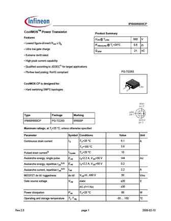
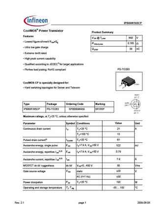
IPB60R600CP CoolMOSTM Power Transistor Product Summary Features V @ Tj,max 650 V DS Lowest figure-of-merit RON x Qg R @ Tj =25 C 0.6 DS(on),max Ultra low gate charge Q 21 nC g,typ Extreme dv/dt rated High peak current capability Qualified according to JEDEC1) for target applications PG-TO263 Pb-free lead plating; RoHS compliant CoolMOS CP is desi
ipb60r060p7.pdf

IPB60R060P7 MOSFET D PAK 600V CoolMOS P7 Power Transistor The CoolMOS 7th generation platform is a revolutionary technology for tab high voltage power MOSFETs, designed according to the superjunction (SJ) principle and pioneered by Infineon Technologies. The 600V CoolMOS P7 series is the successor to the CoolMOS P6 series. It combines the benefits of a fast switching SJ MOS
ipb60r060c7.pdf
MOSFET Metal Oxide Semiconductor Field Effect Transistor CoolMOS C7 600V CoolMOS C7 Power Transistor IPB60R060C7 Data Sheet Rev. 2.0 Final Power Management & Multimarket 600V CoolMOS C7 Power Transistor IPB60R060C7 D PAK 1 Description CoolMOS C7 is a revolutionary technology for high voltage power MOSFETs, designed according to the superjunction (SJ) principle and ta
ipb60r600p6 ipp60r600p6 ipd60r600p6 ipa60r600p6.pdf
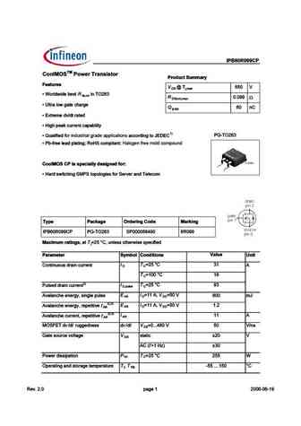
IPB60R600P6, IPP60R600P6, IPD60R600P6, IPA60R600P6 MOSFET D PAK PG-TO 220 DPAK 600V CoolMOS P6 Power Transistor tab tab tab CoolMOS is a revolutionary technology for high voltage power MOSFETs, designed according to the superjunction (SJ) principle and 2 2 pioneered by Infineon Technologies. CoolMOS P6 series combines the 1 1 3 3 experience of the leading SJ MOSFET suppli
ipa60r190c6 ipb60r190c6 ipi60r190c6 ipp60r190c6 ipw60r190c6.pdf
MOSFET Metal Oxide Semiconductor Field Effect Transistor CoolMOS C6 600V 600V CoolMOS C6 Power Transistor IPx60R190C6 Data Sheet Rev. 2.3 Final Power Management & Multimarket 600V CoolMOS C6 Power Transistor IPA60R190C6, IPB60R190C6 IPI60R190C6, IPP60R190C6 IPW60R190C6 1 Description CoolMOS is a revolutionary technology for high voltage power MOSFETs, designed according to

ipb60r090cfd7.pdf

IPB60R090CFD7 MOSFET D PAK 600V CoolMOS CFD7 Power Transistor CoolMOS is a revolutionary technology for high voltage power tab MOSFETs, designed according to the superjunction (SJ) principle and pioneered by Infineon Technologies. The latest CoolMOS CFD7 is the successor to the CoolMOS CFD2 series and is an optimized platform tailored to target soft switching applications s
ipb60r180c7.pdf

IPB60R180C7 MOSFET D PAK 600V CoolMOS C7 Power Transistor CoolMOS C7 is a revolutionary technology for high voltage power tab MOSFETs, designed according to the superjunction (SJ) principle and pioneered by Infineon Technologies. 600V CoolMOS C7 series combines the experience of the leading SJ MOSFET supplier with high class innovation. 2 1 The 600V C7 is the first technolo
ipb60r040cfd7.pdf

IPB60R040CFD7 MOSFET D PAK 600V CoolMOS CFD7 Power Transistor CoolMOS is a revolutionary technology for high voltage power tab MOSFETs, designed according to the superjunction (SJ) principle and pioneered by Infineon Technologies. The latest CoolMOS CFD7 is the successor to the CoolMOS CFD2 series and is an optimized platform tailored to target soft switching applications s

ipb60r190c6.pdf

MOSFET Metal Oxide Semiconductor Field Effect Transistor CoolMOS C6 600V CoolMOS C6 Power Transistor IPx60R190C6 Data Sheet Rev. 2.1, 2010-02-09 Final Industrial & Multimarket 600V CoolMOS C6 Power Transistor IPA60R190C6, IPB60R190C6 IPI60R190C6, IPP60R190C6 IPW60R190C6 1 Description CoolMOS is a revolutionary technology for high voltage power MOSFETs, designed according
ipb60r280p6.pdf

MOSFET Metal Oxide Semiconductor Field Effect Transistor CoolMOS P6 600V CoolMOS P6 Power Transistor IPx60R280P6 Data Sheet Rev. 2.2 Final Power Management & Multimarket 600V CoolMOS P6 Power Transistor IPW60R280P6, IPB60R280P6, IPP60R280P6, IPA60R280P6 TO-247 D PAK TO-220 1 Description tab tab CoolMOS is a revolutionary technology for high voltage power MOSFETs,

ipw60r190p6 ipb60r190p6 ipp60r190p6 ipa60r190p6.pdf

MOSFET Metal Oxide Semiconductor Field Effect Transistor CoolMOS P6 600V CoolMOS P6 Power Transistor IPx60R190P6 Data Sheet Rev. 2.2 Final Power Management & Multimarket 600V CoolMOS P6 Power Transistor IPW60R190P6, IPB60R190P6, IPP60R190P6, IPA60R190P6 TO-247 D PAK TO-220 1 Description tab tab CoolMOS is a revolutionary technology for high voltage power MOSFETs,
ipw60r280p6 ipb60r280p6 ipp60r280p6 ipa60r280p6.pdf

MOSFET Metal Oxide Semiconductor Field Effect Transistor CoolMOS P6 600V CoolMOS P6 Power Transistor IPx60R280P6 Data Sheet Rev. 2.2 Final Power Management & Multimarket 600V CoolMOS P6 Power Transistor IPW60R280P6, IPB60R280P6, IPP60R280P6, IPA60R280P6 TO-247 D PAK TO-220 1 Description tab tab CoolMOS is a revolutionary technology for high voltage power MOSFETs,
ipb60r040c7.pdf
IPB60R040C7 MOSFET D PAK 600V CoolMOS C7 Power Transistor CoolMOS C7 is a revolutionary technology for high voltage power tab MOSFETs, designed according to the superjunction (SJ) principle and pioneered by Infineon Technologies. 600V CoolMOS C7 series combines the experience of the leading SJ MOSFET supplier with high class innovation. 2 1 The 600V C7 is the first technolo
ipb60r125cfd7.pdf
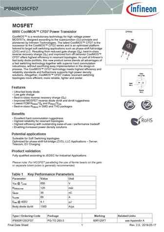
IPB60R125CFD7 MOSFET D PAK 600V CoolMOS CFD7 Power Transistor CoolMOS is a revolutionary technology for high voltage power tab MOSFETs, designed according to the superjunction (SJ) principle and pioneered by Infineon Technologies. The latest CoolMOS CFD7 is the successor to the CoolMOS CFD2 series and is an optimized platform tailored to target soft switching applications s
ipb60r360cfd7.pdf
IPB60R360CFD7 MOSFET D PAK 600V CoolMOS CFD7 Power Transistor CoolMOS is a revolutionary technology for high voltage power tab MOSFETs, designed according to the superjunction (SJ) principle and pioneered by Infineon Technologies. The latest CoolMOS CFD7 is the successor to the CoolMOS CFD2 series and is an optimized platform tailored to target soft switching applications s
ipb60r360p7.pdf

IPB60R360P7 MOSFET D PAK 600V CoolMOS P7 Power Transistor The CoolMOS 7th generation platform is a revolutionary technology for tab high voltage power MOSFETs, designed according to the superjunction (SJ) principle and pioneered by Infineon Technologies. The 600V CoolMOS P7 series is the successor to the CoolMOS P6 series. It combines the benefits of a fast switching SJ MOS
ipb60r199cp.pdf
IPB60R199CP CoolMOS Power Transistor Product Summary Features V @ Tj,max 650 V DS Lowest figure-of-merit RONxQg R 0.199 DS(on),max Ultra low gate charge Q 32 nC g,typ Extreme dv/dt rated High peak current capability Qualified according to JEDEC1) for target applications PG-TO263 Pb-free lead plating; RoHS compliant CoolMOS CP is specially designe
ipb60r520cp.pdf

IPB60R520CP CoolMOSTM Power Transistor Product Summary Features V @ Tj,max 650 V DS Lowest figure-of-merit RON x Qg R @ Tj = 25 C 0.520 DS(on),max Ultra low gate charge Q 24 nC g,typ Extreme dv/dt rated High peak current capability Qualified according to JEDEC1) for target applications PG-TO263 Pb-free lead plating; RoHS compliant CoolMOS CP is d
ipb60r299cpa.pdf
IPB60R299CPA CoolMOSTM Power Transistor Product Summary V 600 V DS R 0.299 DS(on),max Q 22 nC g,typ Features Lowest figure-of-merit Ron x Qg PG-TO263-3 Ultra low gate charge Extreme dv/dt rated High peak current capability Automotive AEC Q101 qualified Green package (RoHS compliant) CoolMOS CPA is specially designed for DC/DC converters for Aut
ipa60r099c6 ipb60r099c6 ipp60r099c6 ipw60r099c6.pdf
MOSFET Metal Oxide Semiconductor Field Effect Transistor CoolMOS C6 600V CoolMOS C6 Power Transistor IPx60R099C6 Data Sheet Rev. 2.1, 2010-02-09 Final Industrial & Multimarket 600V CoolMOS C6 Power Transistor IPA60R099C6, IPB60R099C6 IPP60R099C6 IPW60R099C6 1 Description CoolMOS is a revolutionary technology for high voltage power MOSFETs, designed according to the supe
ipa60r125c6 ipb60r125c6 ipp60r125c6 ipw60r125c6.pdf

MOSFET Metal Oxide Semiconductor Field Effect Transistor CoolMOS C6 600V 600V CoolMOS C6 Power Transistor IPx60R125C6 Data Sheet Rev. 2.3 Final Power Management & Multimarket 600V C IMOS C6 P wer Transist r IPA60R125C6, IPB60R125C6 IPP60R125C6 IPW60R125C6 1 Descripti n CoolMOS is a revolutionary technology for high voltage power MOSFETs designed according to the superj
ipd60r380c6 ipi60r380c6 ipb60r380c6 ipp60r380c6 ipa60r380c6.pdf

MOSFET Metal Oxide Semiconductor Field Effect Transistor CoolMOS C6 600V 600V CoolMOS C6 Power Transistor IPx60R380C6 Data Sheet Rev. 2.3 Final Power Management & Multimarket 600V C IMOS C6 P wer Transist r IPD60R380C6, IPI60R380C6 IPB60R380C6, IPP60R380C6 IPA60R380C6 1 Descripti n CoolMOS is a revolutionary technology for high voltage power MOSFETs designed according
ipb60r120p7.pdf

IPB60R120P7 MOSFET D PAK 600V CoolMOS P7 Power Transistor The CoolMOS 7th generation platform is a revolutionary technology for tab high voltage power MOSFETs, designed according to the superjunction (SJ) principle and pioneered by Infineon Technologies. The 600V CoolMOS P7 series is the successor to the CoolMOS P6 series. It combines the benefits of a fast switching SJ MOS
ipb60r380p6 ipp60r380p6 ipd60r380p6 ipa60r380p6.pdf

IPB60R380P6, IPP60R380P6, IPD60R380P6, IPA60R380P6 MOSFET D PAK PG-TO 220 DPAK 600V CoolMOS P6 Power Transistor tab tab tab CoolMOS is a revolutionary technology for high voltage power MOSFETs, designed according to the superjunction (SJ) principle and 2 2 pioneered by Infineon Technologies. CoolMOS P6 series combines the 1 1 3 3 experience of the leading SJ MOSFET suppli
ipb60r125cpa.pdf

IPB60R125CP CoolMOSTM Power Transistor Product Summary Features V @ Tj,max 650 V DS Lowest figure-of-merit RONxQg R 0.125 DS(on),max Ultra low gate charge Q 53 nC g,typ Extreme dv/dt rated High peak current capability Qualified according to JEDEC1) for target applications PG-TO263 Pb-free lead plating; RoHS compliant CoolMOS CP is specially designe
ipb60r080p7.pdf

IPB60R080P7 MOSFET D PAK 600V CoolMOS P7 Power Transistor The CoolMOS 7th generation platform is a revolutionary technology for tab high voltage power MOSFETs, designed according to the superjunction (SJ) principle and pioneered by Infineon Technologies. The 600V CoolMOS P7 series is the successor to the CoolMOS P6 series. It combines the benefits of a fast switching SJ MOS
ipa60r280c6 ipb60r280c6 ipi60r280c6 ipp60r280c6 ipw60r280c6.pdf
MOSFET Metal Oxide Semiconductor Field Effect Transistor CoolMOS C6 600V 600V CoolMOS C6 Power Transistor IPx60R280C6 Data Sheet Rev. 2.2 Final Power Management & Multimarket 600V C IMOS C6 P wer Transist r IPA60R280C6, IPB60R280C6 IPI60R280C6, IPP60R280C6 IPW60R280C6 1 Descripti n CoolMOS is a revolutionary technology for high voltage power MOSFETs designed according
ipb60r190p6.pdf

Isc N-Channel MOSFET Transistor IPB60R190P6 FEATURES With To-263(D2PAK) package Low input capacitance and gate charge Low gate input resistance 100% avalanche tested Minimum Lot-to-Lot variations for robust device performance and reliable operation APPLICATIONS Switching applications ABSOLUTE MAXIMUM RATINGS(T =25 ) a SYMBOL PARAMETER VALUE UNIT V Drain-Source V
ipb60r600p6.pdf

Isc N-Channel MOSFET Transistor IPB60R600P6 FEATURES With To-263(D2PAK) package Low input capacitance and gate charge Low gate input resistance 100% avalanche tested Minimum Lot-to-Lot variations for robust device performance and reliable operation APPLICATIONS Switching applications ABSOLUTE MAXIMUM RATINGS(T =25 ) a SYMBOL PARAMETER VALUE UNIT V Drain-Source V
ipb60r099cp.pdf

Isc N-Channel MOSFET Transistor IPB60R099CP FEATURES With To-263(D2PAK) package Low input capacitance and gate charge Low gate input resistance 100% avalanche tested Minimum Lot-to-Lot variations for robust device performance and reliable operation APPLICATIONS Switching applications ABSOLUTE MAXIMUM RATINGS(T =25 ) a SYMBOL PARAMETER VALUE UNIT V Drain-Source V
ipb60r099p7.pdf

Isc N-Channel MOSFET Transistor IPB60R099P7 FEATURES With To-263(D2PAK) package Low input capacitance and gate charge Low gate input resistance 100% avalanche tested Minimum Lot-to-Lot variations for robust device performance and reliable operation APPLICATIONS Switching applications ABSOLUTE MAXIMUM RATINGS(T =25 ) a SYMBOL PARAMETER VALUE UNIT V Drain-Source V
ipb60r299cp.pdf

Isc N-Channel MOSFET Transistor IPB60R299CP FEATURES With To-263(D2PAK) package Low input capacitance and gate charge Low gate input resistance 100% avalanche tested Minimum Lot-to-Lot variations for robust device performance and reliable operation APPLICATIONS Switching applications ABSOLUTE MAXIMUM RATINGS(T =25 ) a SYMBOL PARAMETER VALUE UNIT V Drain-Source V
ipb60r160c6.pdf

Isc N-Channel MOSFET Transistor IPB60R160C6 FEATURES With To-263(D2PAK) package Low input capacitance and gate charge Low gate input resistance 100% avalanche tested Minimum Lot-to-Lot variations for robust device performance and reliable operation APPLICATIONS Switching applications ABSOLUTE MAXIMUM RATINGS(T =25 ) a SYMBOL PARAMETER VALUE UNIT V Drain-Source V
ipb60r165cp.pdf
INCHANGE Semiconductor isc N-Channel MOSFET Transistor IPB60R165CP FEATURES With TO-263(D2PAK) packaging Ultra-fast body diode High speed switching Very high commutation ruggedness Easy to use 100% avalanche tested Minimum Lot-to-Lot variations for robust device performance and reliable operationz APPLICATIONS PFC stages, hard switching PWM stages and resonant sw
ipb60r125c6.pdf

Isc N-Channel MOSFET Transistor IPB60R125C6 FEATURES With To-263(D2PAK) package Low input capacitance and gate charge Low gate input resistance 100% avalanche tested Minimum Lot-to-Lot variations for robust device performance and reliable operation APPLICATIONS Switching applications ABSOLUTE MAXIMUM RATINGS(T =25 ) a SYMBOL PARAMETER VALUE UNIT V Drain-Source V
ipb60r250cp.pdf

Isc N-Channel MOSFET Transistor IPB60R250CP FEATURES With To-263(D2PAK) package Low input capacitance and gate charge Low gate input resistance 100% avalanche tested Minimum Lot-to-Lot variations for robust device performance and reliable operation APPLICATIONS Switching applications ABSOLUTE MAXIMUM RATINGS(T =25 ) a SYMBOL PARAMETER VALUE UNIT V Drain-Source V
ipb60r160p6.pdf

Isc N-Channel MOSFET Transistor IPB60R160P6 FEATURES With To-263(D2PAK) package Low input capacitance and gate charge Low gate input resistance 100% avalanche tested Minimum Lot-to-Lot variations for robust device performance and reliable operation APPLICATIONS Switching applications ABSOLUTE MAXIMUM RATINGS(T =25 ) a SYMBOL PARAMETER VALUE UNIT V Drain-Source V
ipb60r099c7.pdf

Isc N-Channel MOSFET Transistor IPB60R099C7 FEATURES With To-263(D2PAK) package Low input capacitance and gate charge Low gate input resistance 100% avalanche tested Minimum Lot-to-Lot variations for robust device performance and reliable operation APPLICATIONS Switching applications ABSOLUTE MAXIMUM RATINGS(T =25 ) a SYMBOL PARAMETER VALUE UNIT V Drain-Source V
ipb60r380p6.pdf

Isc N-Channel MOSFET Transistor IPB60R380P6 FEATURES With To-263(D2PAK) package Low input capacitance and gate charge Low gate input resistance 100% avalanche tested Minimum Lot-to-Lot variations for robust device performance and reliable operation APPLICATIONS Switching applications ABSOLUTE MAXIMUM RATINGS(T =25 ) a SYMBOL PARAMETER VALUE UNIT V Drain-Source V
ipb60r180p7.pdf

Isc N-Channel MOSFET Transistor IPB60R180P7 FEATURES With To-263(D2PAK) package Low input capacitance and gate charge Low gate input resistance 100% avalanche tested Minimum Lot-to-Lot variations for robust device performance and reliable operation APPLICATIONS Switching applications ABSOLUTE MAXIMUM RATINGS(T =25 ) a SYMBOL PARAMETER VALUE UNIT V Drain-Source V
ipb60r125cp.pdf

Isc N-Channel MOSFET Transistor IPB60R125CP FEATURES With To-263(D2PAK) package Low input capacitance and gate charge Low gate input resistance 100% avalanche tested Minimum Lot-to-Lot variations for robust device performance and reliable operation APPLICATIONS Switching applications ABSOLUTE MAXIMUM RATINGS(T =25 ) a SYMBOL PARAMETER VALUE UNIT V Drain-Source V
ipb60r230p6.pdf
Isc N-Channel MOSFET Transistor IPB60R230P6 FEATURES With To-263(D2PAK) package Low input capacitance and gate charge Low gate input resistance 100% avalanche tested Minimum Lot-to-Lot variations for robust device performance and reliable operation APPLICATIONS Switching applications ABSOLUTE MAXIMUM RATINGS(T =25 ) a SYMBOL PARAMETER VALUE UNIT V Drain-Source V
ipb60r385cp.pdf

Isc N-Channel MOSFET Transistor IPB60R385CP FEATURES With To-263(D2PAK) package Low input capacitance and gate charge Low gate input resistance 100% avalanche tested Minimum Lot-to-Lot variations for robust device performance and reliable operation APPLICATIONS Switching applications ABSOLUTE MAXIMUM RATINGS(T =25 ) a SYMBOL PARAMETER VALUE UNIT V Drain-Source V
ipb60r600c6.pdf

Isc N-Channel MOSFET Transistor IPB60R600C6 FEATURES With To-263(D2PAK) package Low input capacitance and gate charge Low gate input resistance 100% avalanche tested Minimum Lot-to-Lot variations for robust device performance and reliable operation APPLICATIONS Switching applications ABSOLUTE MAXIMUM RATINGS(T =25 ) a SYMBOL PARAMETER VALUE UNIT V Drain-Source V
ipb60r280p7.pdf

Isc N-Channel MOSFET Transistor IPB60R280P7 FEATURES With To-263(D2PAK) package Low input capacitance and gate charge Low gate input resistance 100% avalanche tested Minimum Lot-to-Lot variations for robust device performance and reliable operation APPLICATIONS Switching applications ABSOLUTE MAXIMUM RATINGS(T =25 ) a SYMBOL PARAMETER VALUE UNIT V Drain-Source V
ipb60r600cp.pdf

Isc N-Channel MOSFET Transistor IPB60R600CP FEATURES With To-263(D2PAK) package Low input capacitance and gate charge Low gate input resistance 100% avalanche tested Minimum Lot-to-Lot variations for robust device performance and reliable operation APPLICATIONS Switching applications ABSOLUTE MAXIMUM RATINGS(T =25 ) a SYMBOL PARAMETER VALUE UNIT V Drain-Source V
ipb60r060p7.pdf

Isc N-Channel MOSFET Transistor IPB60R060P7 FEATURES With To-263(D2PAK) package Low input capacitance and gate charge Low gate input resistance 100% avalanche tested Minimum Lot-to-Lot variations for robust device performance and reliable operation APPLICATIONS Switching applications ABSOLUTE MAXIMUM RATINGS(T =25 ) a SYMBOL PARAMETER VALUE UNIT V Drain-Source V
ipb60r060c7.pdf
Isc N-Channel MOSFET Transistor IPB60R060C7 FEATURES With To-263(D2PAK) package Low input capacitance and gate charge Low gate input resistance 100% avalanche tested Minimum Lot-to-Lot variations for robust device performance and reliable operation APPLICATIONS Switching applications ABSOLUTE MAXIMUM RATINGS(T =25 ) a SYMBOL PARAMETER VALUE UNIT V Drain-Source V
ipb60r380c6.pdf

Isc N-Channel MOSFET Transistor IPB60R380C6 FEATURES With To-263(D2PAK) package Low input capacitance and gate charge Low gate input resistance 100% avalanche tested Minimum Lot-to-Lot variations for robust device performance and reliable operation APPLICATIONS Switching applications ABSOLUTE MAXIMUM RATINGS(T =25 ) a SYMBOL PARAMETER VALUE UNIT V Drain-Source V
ipb60r180c7.pdf

Isc N-Channel MOSFET Transistor IPB60R180C7 FEATURES With To-263(D2PAK) package Low input capacitance and gate charge Low gate input resistance 100% avalanche tested Minimum Lot-to-Lot variations for robust device performance and reliable operation APPLICATIONS Switching applications ABSOLUTE MAXIMUM RATINGS(T =25 ) a SYMBOL PARAMETER VALUE UNIT V Drain-Source V
ipb60r280c6.pdf

Isc N-Channel MOSFET Transistor IPB60R280C6 FEATURES With To-263(D2PAK) package Low input capacitance and gate charge Low gate input resistance 100% avalanche tested Minimum Lot-to-Lot variations for robust device performance and reliable operation APPLICATIONS Switching applications ABSOLUTE MAXIMUM RATINGS(T =25 ) a SYMBOL PARAMETER VALUE UNIT V Drain-Source V
ipb60r190c6.pdf
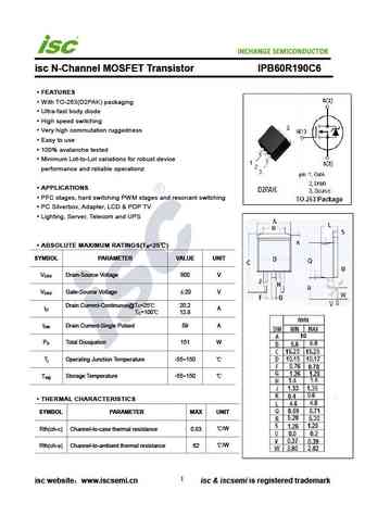
INCHANGE Semiconductor isc N-Channel MOSFET Transistor IPB60R190C6 FEATURES With TO-263(D2PAK) packaging Ultra-fast body diode High speed switching Very high commutation ruggedness Easy to use 100% avalanche tested Minimum Lot-to-Lot variations for robust device performance and reliable operationz APPLICATIONS PFC stages, hard switching PWM stages and resonant sw
ipb60r280p6.pdf
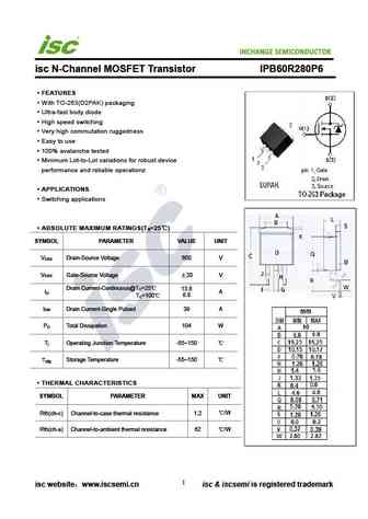
INCHANGE Semiconductor isc N-Channel MOSFET Transistor IPB60R280P6 FEATURES With TO-263(D2PAK) packaging Ultra-fast body diode High speed switching Very high commutation ruggedness Easy to use 100% avalanche tested Minimum Lot-to-Lot variations for robust device performance and reliable operationz APPLICATIONS Switching applications ABSOLUTE MAXIMUM RATINGS(T
ipb60r099c6.pdf

Isc N-Channel MOSFET Transistor IPB60R099C6 FEATURES With To-263(D2PAK) package Low input capacitance and gate charge Low gate input resistance 100% avalanche tested Minimum Lot-to-Lot variations for robust device performance and reliable operation APPLICATIONS Switching applications ABSOLUTE MAXIMUM RATINGS(T =25 ) a SYMBOL PARAMETER VALUE UNIT V Drain-Source V
ipb60r040c7.pdf

Isc N-Channel MOSFET Transistor IPB60R040C7 FEATURES With To-263(D2PAK) package Low input capacitance and gate charge Low gate input resistance 100% avalanche tested Minimum Lot-to-Lot variations for robust device performance and reliable operation APPLICATIONS Switching applications ABSOLUTE MAXIMUM RATINGS(T =25 ) a SYMBOL PARAMETER VALUE UNIT V Drain-Source V
ipb60r360p7.pdf

Isc N-Channel MOSFET Transistor IPB60R360P7 FEATURES With To-263(D2PAK) package Low input capacitance and gate charge Low gate input resistance 100% avalanche tested Minimum Lot-to-Lot variations for robust device performance and reliable operation APPLICATIONS Switching applications ABSOLUTE MAXIMUM RATINGS(T =25 ) a SYMBOL PARAMETER VALUE UNIT V Drain-Source V
ipb60r199cp.pdf

Isc N-Channel MOSFET Transistor IPB60R199CP FEATURES With To-263(D2PAK) package Low input capacitance and gate charge Low gate input resistance 100% avalanche tested Minimum Lot-to-Lot variations for robust device performance and reliable operation APPLICATIONS Switching applications ABSOLUTE MAXIMUM RATINGS(T =25 ) a SYMBOL PARAMETER VALUE UNIT V Drain-Source V
ipb60r520cp.pdf

Isc N-Channel MOSFET Transistor IPB60R520CP FEATURES With To-263(D2PAK) package Low input capacitance and gate charge Low gate input resistance 100% avalanche tested Minimum Lot-to-Lot variations for robust device performance and reliable operation APPLICATIONS Switching applications ABSOLUTE MAXIMUM RATINGS(T =25 ) a SYMBOL PARAMETER VALUE UNIT V Drain-Source V
ipb60r330p6.pdf

Isc N-Channel MOSFET Transistor IPB60R330P6 FEATURES With To-263(D2PAK) package Low input capacitance and gate charge Low gate input resistance 100% avalanche tested Minimum Lot-to-Lot variations for robust device performance and reliable operation APPLICATIONS Switching applications ABSOLUTE MAXIMUM RATINGS(T =25 ) a SYMBOL PARAMETER VALUE UNIT V Drain-Source V
ipb60r120p7.pdf

Isc N-Channel MOSFET Transistor IPB60R120P7 FEATURES With To-263(D2PAK) package Low input capacitance and gate charge Low gate input resistance 100% avalanche tested Minimum Lot-to-Lot variations for robust device performance and reliable operation APPLICATIONS Switching applications ABSOLUTE MAXIMUM RATINGS(T =25 ) a SYMBOL PARAMETER VALUE UNIT V Drain-Source V
ipb60r080p7.pdf

Isc N-Channel MOSFET Transistor IPB60R080P7 FEATURES With To-263(D2PAK) package Low input capacitance and gate charge Low gate input resistance 100% avalanche tested Minimum Lot-to-Lot variations for robust device performance and reliable operation APPLICATIONS Switching applications ABSOLUTE MAXIMUM RATINGS(T =25 ) a SYMBOL PARAMETER VALUE UNIT V Drain-Source V
Otros transistores... IPB60R280C6, IPB60R299CP, IPB60R299CPA, IPB60R380C6, IPB60R385CP, IPB60R520CP, IPB60R600C6, IPB60R600CP, 50N06, IPB65R280C6, IPB65R280E6, IPB65R380C6, IPB65R600C6, IPB65R660CFD, IPB70N04S4-06, IPB79CN10NG, IPB80N04S4-03
History: IRF7404TR
🌐 : EN ES РУ

Liste
Recientemente añadidas las descripciónes de los transistores:
MOSFET: AUP060N055 | AUP056N10 | AUP056N08BGL | AUP052N085 | AUP045N12 | AUP039N10 | AUP034N10 | AUP034N06 | AUP033N08BG | AUP026N085 | AUN084N10 | AUN065N10 | AUN063N10 | AUN062N08BG | AUN060N08AG | AUN053N10
Popular searches
2sd667 | 2sc1111 | bc239 transistor equivalent | 3sk41 | 2sc2240 transistor | c3198 | 2sc793 | 2sd313 replacement