IPP04CN10NG Datasheet. Equivalente. Reemplazo. Hoja de especificaciones. Principales características
Número de Parte: IPP04CN10NG 📄📄
Tipo de FET: MOSFET
Polaridad de transistor: N
ESPECIFICACIONES MÁXIMAS
Pdⓘ - Máxima disipación de potencia: 300 W
|Vds|ⓘ - Voltaje máximo drenador-fuente: 100 V
|Vgs|ⓘ - Voltaje máximo fuente-puerta: 20 V
|Id|ⓘ - Corriente continua de drenaje: 100 A
Tjⓘ - Temperatura máxima de unión: 175 °C
CARACTERÍSTICAS ELÉCTRICAS
trⓘ - Tiempo de subida: 78 nS
Cossⓘ - Capacitancia de salida: 1590 pF
RDSonⓘ - Resistencia estado encendido drenaje a fuente: 0.0042 Ohm
Encapsulados: TO220
📄📄 Copiar
Búsqueda de reemplazo de IPP04CN10NG MOSFET
- Selecciónⓘ de transistores por parámetros
IPP04CN10NG datasheet
..1. Size:874K infineon
ipb04cn10ng ipi04cn10ng ipp04cn10ng ipp04cn10n .pdf 

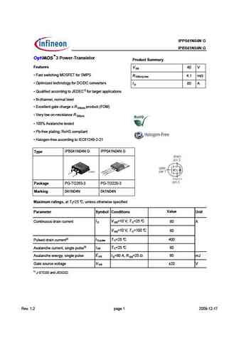
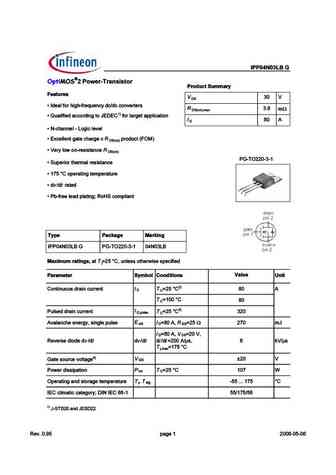
IPB04CN10N G IPI04CN10N G IPP04CN10N G 2 Power-Transistor Product Summary Features V 1 D R ( 492??6= ?@C>2= =6G6= R m - @? >2I .) R I46==6?E 82E6 492C86 I R AC@5F4E !) ' D n) I 1 D R /6CJ =@H @? C6D DE2?46 R D n) R U @A6C2E ?8 E6>A6C2EFC6 R *3 7C66 =625 A=2E ?8 , @#- 4@>A= 2?E 1) R + F2= 7 65 244@C5 ?8 E@ % 7@C E2C86E 2AA= 42E @? R $562= 7@C 9 89 7C6BF6?4J DH E4
4.1. Size:871K infineon
ipb04cn10ng ipi04cn10n ipp04cn10n.pdf
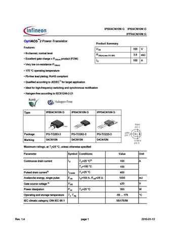
IPB04CN10N G IPI04CN10N G IPP04CN10N G 2 Power-Transistor Product Summary Features V 1 D R ( 492??6= ?@C>2= =6G6= R m - @? >2I .) R I46==6?E 82E6 492C86 I R AC@5F4E !) ' D n) I 1 D R /6CJ =@H @? C6D DE2?46 R D n) R U @A6C2E ?8 E6>A6C2EFC6 R *3 7C66 =625 A=2E ?8 , @#- 4@>A= 2?E 1) R + F2= 7 65 244@C5 ?8 E@ % 7@C E2C86E 2AA= 42E @? R $562= 7@C 9 89 7C6BF6?4J DH E4
4.2. Size:246K inchange semiconductor
ipp04cn10n.pdf
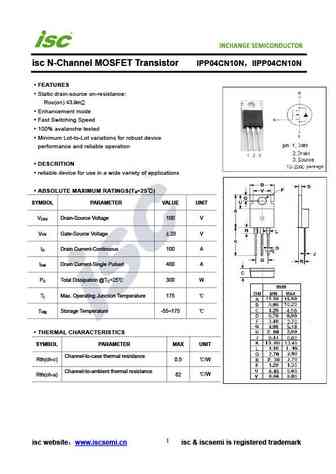
NCHANGE Semicon Iductor isc N-Channel MOSFET Transistor IPP04CN10N IIPP04CN10N FEATURES Static drain-source on-resistance RDS(on) 3.9m Enhancement mode Fast Switching Speed 100% avalanche tested Minimum Lot-to-Lot variations for robust device performance and reliable operation DESCRITION reliable device for use in a wide variety of applications ABSOLUTE MA
9.1. Size:484K infineon
ipb037n06n3g ipi040n06n3g ipp040n06n3g.pdf
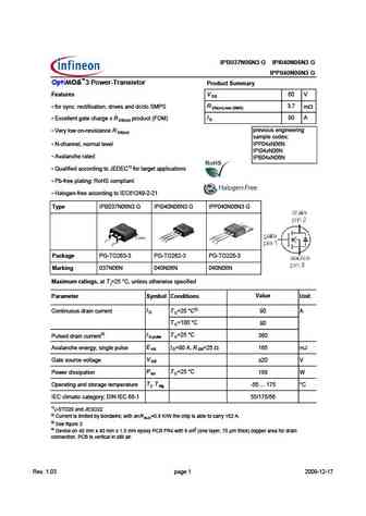
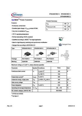
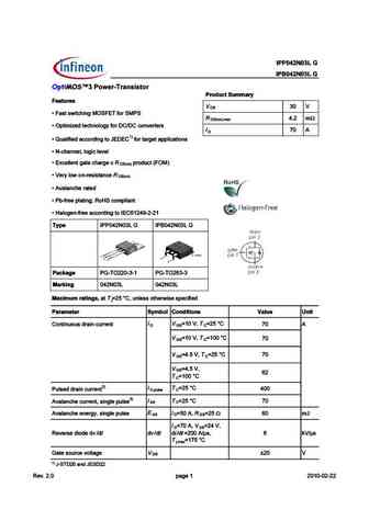
Type IPB037N06N3 G IPI040N06N3 G IPP040N06N3 G OptiMOS 3 Power-Transistor Product Summary Features V 60 V DS R 3.7 for sync. rectification, drives and dc/dc SMPS m DS(on),max (SMD) I 90 A Excellent gate charge x R product (FOM) D DS(on) previous engineering Very low on-resistance R DS(on) sample codes N-channel, normal level IPP04xN06N IPI04xN06N Ava
9.3. Size:508K infineon
ipb038n12n3-g ipi041n12n3-g ipp041n12n3-g.pdf
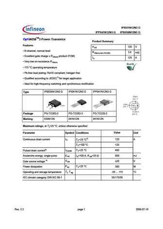
IPI041N12N3 G IPP041N12N3 G IPB038N12N3 G OptiMOSTM3 Power-Transistor Product Summary Features V 120 V DS N-channel, normal level R 3.8 m DS(on),max (TO-263) Excellent gate charge x R product (FOM) DS(on) I 120 A D Very low on-resistance R DS(on) 175 C operating temperature Pb-free lead plating; RoHS compliant, halogen free Qualified according to
9.5. Size:566K infineon
ipp048n12n3g.pdf
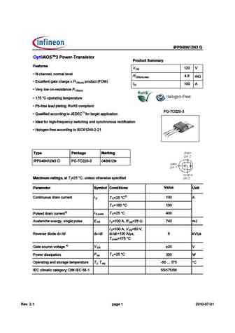
$$ " " $;B1= '=- >5>?;= $=;0@/? &@99-=D Features 120 V DS R ( 492??6= ?@C>2= =6G6= 4.8 m - @? >2I R I46==6?E 82E6 492C86 I AC@5F4E !) ' DS(on) 100 A D R /6CJ =@H @? C6D DE2?46 DS(on) R U @A6C2E ?8 E6>A6C2EFC6 R *3 7C66 =625 A=2E ?8 , @#- 4@>A= 2?E PG TO220 1) R + F2= 7 65 244@C5 ?8 E@ % 7@C E2C86E 2AA= 42E @? R $562= 7@C 9 89 7C6BF6?4J DH E49 ?8 2?5 DJ?49C@?
9.6. Size:612K infineon
ipp042n03l .pdf

pe %% # ! % # ! F % (>.;?6?@ %>E Features D Q 2CD CG D49 ?8 ') - . 7@B -'*- 4 m - @? >2H Q ) AD > J65 D649?@=@8I 7@B 4@?F6BD6BC 7 D 1) Q + E2= 7 65 244@B5 ?8 D@ $ 7@B D2B86D 2AA= 42D @?C Q ( 492??6= =@8 4 =6F6= Q H46==6?D 82D6 492B86 H AB@5E4D ) ' D n) Q /6BI =@G @? B6C CD2?46 D n) Q F2=2?496 B2D65 Q *3 7B66 A=2D ?8 , @"- 4@>A= 2?D Q "2=@86
9.7. Size:1653K infineon
ipp040n06n3g.pdf
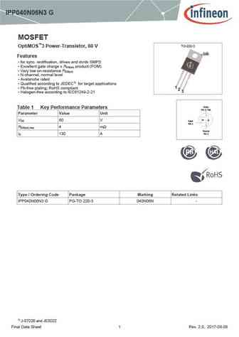
IPP040N06N3 G MOSFET TO-220-3 OptiMOS 3 Power-Transistor, 60 V tab Features for sync. rectification, drives and dc/dc SMPS Excellent gate charge x R product (FOM) DS(on) Very low on-resistance R DS(on) N-channel, normal level Avalanche rated Qualified according to JEDEC1) for target applications Pb-free plating; RoHS compliant Halogen-free accordi
9.8. Size:535K infineon
ipp04n03lb rev0.95.pdf
$$ " $;B1= '=- >5>?;= $=;0@/? &@99-=D Features D S $673> 8AD ;9 8D7CG7@5K 65 65 5A@H7DF7DE m D n) m x 1) S , G3>;8;76 355AD6;@9 FA % 8AD F3D97F 3BB>;53F;A@ D S ) 5 3@@7> 'A9;5 >7H7> S J57>>7@F 93F7 5 3D97 J BDA6G5F !* ( D n) S 07DK >AI A@ D7E;EF3@57 D n) G O 1 S .GB7D;AD F 7D?3> D7E;EF3@57 S V AB7D3F;@9 F7?B7D3FGD7 S 6v t D3F76 S +4 8D77 >736 B>3F;@9
9.9. Size:611K infineon
ipp042n03l.pdf
pe %% # ! % # ! F % (>.;?6?@ %>E Features D Q 2CD CG D49 ?8 ') - . 7@B -'*- 4 m - @? >2H Q ) AD > J65 D649?@=@8I 7@B 4@?F6BD6BC 7 D 1) Q + E2= 7 65 244@B5 ?8 D@ $ 7@B D2B86D 2AA= 42D @?C Q ( 492??6= =@8 4 =6F6= Q H46==6?D 82D6 492B86 H AB@5E4D ) ' D n) Q /6BI =@G @? B6C CD2?46 D n) Q F2=2?496 B2D65 Q *3 7B66 A=2D ?8 , @"- 4@>A= 2?D Q "2=@86
9.10. Size:458K infineon
ipp040n06n.pdf
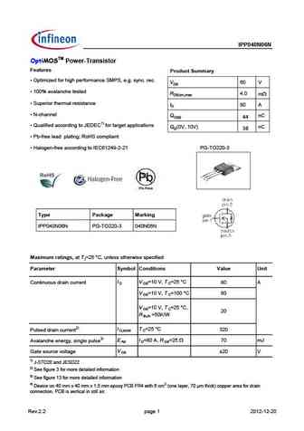
Type IPP040N06N OptiMOSTM Power-Transistor Features Product Summary Optimized for high performance SMPS, e.g. sync. rec. VDS 60 V 100% avalanche tested RDS(on),max 4.0 mW Superior thermal resistance ID 80 A N-channel QOSS nC 44 Qualified according to JEDEC1) for target applications QG(0V..10V) nC 38 Pb-free lead plating; RoHS compliant Hal
9.11. Size:734K infineon
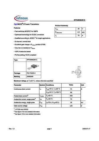
ipb048n06lg ipp048n06lg5.pdf
IPP048N06L G IPB048N06L G Power-Transistor Product Summary Features V D P ?A 61BC BF9C389>7 3?>E5AC5AB 1>4 BH>3 A53C96931C9?> R 4 4 m , ?> =1G ,' E5AB9?> P ( 381>>581>35=5>C
9.12. Size:873K infineon
ipi041n12n3g ipp041n12n3g ipb038n12n3g.pdf
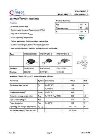
IPI041N12N3 G IPP041N12N3 G IPB038N12N3 G OptiMOSTM3 Power-Transistor Product Summary Features VDS 120 V N-channel, normal level RDS(on),max (TO-263) 3.8 mW Excellent gate charge x R product (FOM) DS(on) ID 120 A Very low on-resistance R DS(on) 175 C operating temperature Pb-free lead plating; RoHS compliant, halogen free Qualified according to JE
9.13. Size:565K infineon
ipp048n04n.pdf
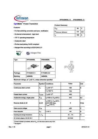
pe $$ " " $;B1= '=- >5>?;= $=;0@/? &@99-=D Features 4 D R 3DE DH;E5 ;@9 &( , - 8AC ,&), 4 m , A@ ?3I R ( BE;?;K76 E75 @A>A9J 8AC 5A@G7CE7CD 7 D 1) R * F3>;8;76 355AC6;@9 EA $ 8AC E3C97E 3BB>;53E;A@D R ' 5 3@@7> @AC?3> >7G7> R I57>>7@E 93E7 5 3C97 I BCA6F5E ( & D n) R .7CJ >AH A@ C7D;DE3@57 D n) R G3>3@5 7 E7DE76 R )4 8C77 B>3E;@9 + A", 5A?B>;3@E Type #))
9.14. Size:748K infineon
ipp045n10n3g.pdf

IPB042N10N3 G IPI045N10N3 G IPP045N10N3 G 3 Power-Transistor Product Summary Features V 1 D Q ' 381>>5?B=1
9.15. Size:1926K cn vbsemi
ipp048n06.pdf
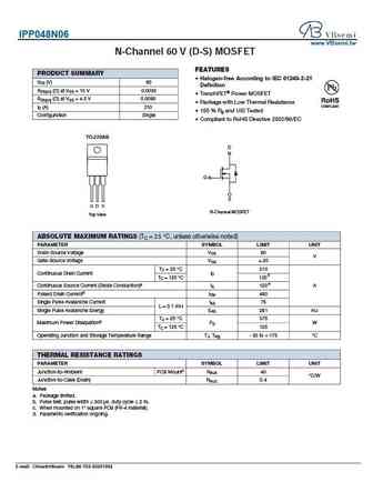
IPP048N06 www.VBsemi.tw N-Channel 60 V (D-S) MOSFET FEATURES PRODUCT SUMMARY Halogen-free According to IEC 61249-2-21 VDS (V) 60 Definition RDS(on) ( ) at VGS = 10 V 0.0035 TrenchFET Power MOSFET RDS(on) ( ) at VGS = 4.5 V 0.0090 Package with Low Thermal Resistance ID (A) 210 100 % Rg and UIS Tested Configuration Single Compliant to RoHS Directive 2002/9
9.16. Size:2138K cn vbsemi
ipp048n04.pdf
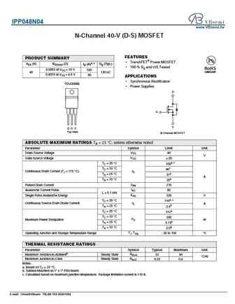
IPP048N04 www.VBsemi.tw N-Channel 40-V (D-S) MOSFET FEATURES PRODUCT SUMMARY TrenchFET Power MOSFET VDS (V) RDS(on) ( ) ID (A)a, c Qg (Typ.) 100 % Rg and UIS Tested RoHS 0.0055 at VGS = 10 V 100 COMPLIANT 40 130 nC 0.0070 at VGS = 4.5 V 90 APPLICATIONS Synchronous Rectification TO-220AB Power Supplies D G S G D S Top View N-Channel MOSFET ABSOLUT
9.17. Size:245K inchange semiconductor
ipp041n04n.pdf
isc N-Channel MOSFET Transistor IPP041N04N,IIPP041N04N FEATURES Static drain-source on-resistance RDS(on) 4.1m Enhancement mode Fast Switching Speed 100% avalanche tested Minimum Lot-to-Lot variations for robust device performance and reliable operation DESCRITION Fast switching for SMPS Optimized technology for DC/DC converters ABSOLUTE MAXIMUM RATINGS(T
9.18. Size:246K inchange semiconductor
ipp042n03l.pdf
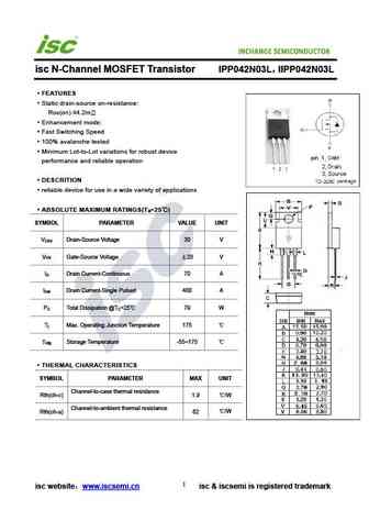
INCHANGE Semiconductor isc N-Channel MOSFET Transistor IPP042N03L IIPP042N03L FEATURES Static drain-source on-resistance RDS(on) 4.2m Enhancement mode Fast Switching Speed 100% avalanche tested Minimum Lot-to-Lot variations for robust device performance and reliable operation DESCRITION reliable device for use in a wide variety of applications ABSOLUTE
9.19. Size:246K inchange semiconductor
ipp040n06n.pdf
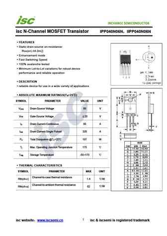
INCHANGE Semiconductor isc N-Channel MOSFET Transistor IPP040N06N IIPP040N06N FEATURES Static drain-source on-resistance RDS(on) 4.0m Enhancement mode Fast Switching Speed 100% avalanche tested Minimum Lot-to-Lot variations for robust device performance and reliable operation DESCRITION reliable device for use in a wide variety of applications ABSOLUTE MAX
9.20. Size:245K inchange semiconductor
ipp048n12n3.pdf
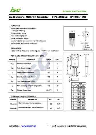
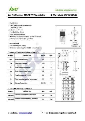
isc N-Channel MOSFET Transistor IPP048N12N3 IIPP048N12N3 FEATURES Static drain-source on-resistance RDS(on) 4.8m Enhancement mode Fast Switching Speed 100% avalanche tested Minimum Lot-to-Lot variations for robust device performance and reliable operation DESCRITION Ideal for high-frequency switching and synchronous rectification ABSOLUTE MAXIMUM RATINGS(T
9.21. Size:246K inchange semiconductor
ipp040n06n3.pdf

INCHANGE Semiconductor isc N-Channel MOSFET Transistor IPP040N06N3 IIPP040N06N3 FEATURES Static drain-source on-resistance RDS(on) 3.7m Enhancement mode Fast Switching Speed 100% avalanche tested Minimum Lot-to-Lot variations for robust device performance and reliable operation DESCRITION reliable device for use in a wide variety of applications ABSOLUTE M
9.22. Size:246K inchange semiconductor
ipp048n04n.pdf
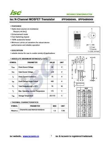
INCHANGE Semiconductor isc N-Channel MOSFET Transistor IPP048N04N IIPP048N04N FEATURES Static drain-source on-resistance RDS(on) 4.8m Enhancement mode Fast Switching Speed 100% avalanche tested Minimum Lot-to-Lot variations for robust device performance and reliable operation DESCRITION reliable device for use in a wide variety of applications ABSOLUTE MAX
9.23. Size:245K inchange semiconductor
ipp041n12n3.pdf

isc N-Channel MOSFET Transistor IPP041N12N3 IIPP041N12N3 FEATURES Static drain-source on-resistance RDS(on) 4.1m Enhancement mode Fast Switching Speed 100% avalanche tested Minimum Lot-to-Lot variations for robust device performance and reliable operation DESCRITION Ideal for high-frequency switching and synchronous rectification ABSOLUTE MAXIMUM RATINGS(
Otros transistores... IPP039N04LG, IPP040N06N3G, IPP041N04NG, IPP041N12N3G, IPP042N03LG, IPP045N10N3G, IPP048N04NG, IPP048N12N3G, IRFP250, IPP04N03LBG, IPP052N06L3G, IPP052NE7N3G, IPP055N03LG, IPP057N06N3G, IPP057N08N3G, IPP05CN10LG, IPP05CN10NG