IPW90R1K2C3 MOSFET Equivalente. Reemplazo. Hoja de especificaciones. Principales características
Número de Parte: IPW90R1K2C3
Tipo de FET: MOSFET
Polaridad de transistor: N
ESPECIFICACIONES MÁXIMAS
Pdⓘ - Máxima disipación de potencia: 83 W
|Vds|ⓘ - Voltaje máximo drenador-fuente: 900 V
|Vgs|ⓘ - Voltaje máximo fuente-puerta: 20 V
|Id|ⓘ - Corriente continua de drenaje: 5.1 A
Tjⓘ - Temperatura máxima de unión: 150 °C
CARACTERÍSTICAS ELÉCTRICAS
trⓘ - Tiempo de subida: 20 nS
Cossⓘ - Capacitancia de salida: 35 pF
RDSonⓘ - Resistencia estado encendido drenaje a fuente: 1.2 Ohm
Encapsulados: TO247
Búsqueda de reemplazo de IPW90R1K2C3 MOSFET
- Selecciónⓘ de transistores por parámetros
IPW90R1K2C3 datasheet
ipw90r1k2c3.pdf
IPW90R1K2C3 C IMOS # A0IN U . J6A>;> 9 for industrial grade applications 688DG9>CC6CI U 2 AIG6 ADL
ipw90r1k2c3.pdf
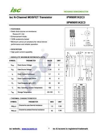
isc N-Channel MOSFET Transistor IPW90R1K2C3 IIPW90R1K2C3 FEATURES Static drain-source on-resistance RDS(on) 1.2 Enhancement mode 100% avalanche tested Minimum Lot-to-Lot variations for robust device performance and reliable operation DESCRITION High peak current capability ABSOLUTE MAXIMUM RATINGS(T =25 ) a SYMBOL PARAMETER VALUE UNIT V Drain-Source Voltag
ipw90r1k0c3.pdf

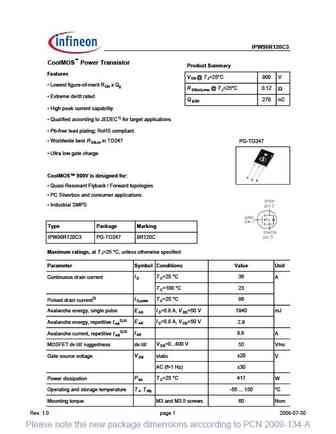
IPW90R1K0C3 CoolMOS Power Transistor Product Summary Features V @ T =25 C 900 V DS J Lowest figure-of-merit RON x Qg R @ T = 25 C 1.0 DS(on),max J Extreme dv/dt rated Q 34 nC g,typ High peak current capability Qualified according to JEDEC1) for target applications Pb-free lead plating; RoHS compliant PG-TO247 Ultra low gate charge CoolMOS 90


Otros transistores... IPW60R299CP, IPW65R070C6, IPW65R080CFD, IPW65R280C6, IPW65R280E6, IPW65R660CFD, IPW90R120C3, IPW90R1K0C3, 2N7000, IPW90R340C3, IPW90R500C3, IPW90R800C3, SPA02N80C3, SPA03N60C3, SPA04N50C3, SPA04N60C3, SPA04N80C3
History: IPW65R280E6
🌐 : EN ES РУ

Liste
Recientemente añadidas las descripciónes de los transistores:
MOSFET: CM4407 | CM3407 | CM3400 | SVF11N65F | SVF11N65T | FKBB3105 | EHBA036R1 | CRTT067N10N | AP6NA3R2MT | AP65SA145DDT8 | AP4NAR95CMT-A | AP4024GEMT-HF | AP3P050AH | AP3P020H | AP3N9R5YT | AP3N9R5MT
Popular searches
bc639 equivalent | bd138 transistor equivalent | c1096 transistor | c1345 transistor | jcs640c | kn2907a | ncep028n85 datasheet | sw50n06