IRFR18N15D MOSFET Equivalente. Reemplazo. Hoja de especificaciones. Principales características
Número de Parte: IRFR18N15D
Tipo de FET: MOSFET
Polaridad de transistor: N
ESPECIFICACIONES MÁXIMAS
Pdⓘ - Máxima disipación de potencia: 110 W
|Vds|ⓘ - Voltaje máximo drenador-fuente: 150 V
|Vgs|ⓘ - Voltaje máximo fuente-puerta: 30 V
|Id|ⓘ - Corriente continua de drenaje: 18 A
Tjⓘ - Temperatura máxima de unión: 175 °C
CARACTERÍSTICAS ELÉCTRICAS
trⓘ - Tiempo de subida: 25 nS
Cossⓘ - Capacitancia de salida: 190 pF
RDSonⓘ - Resistencia estado encendido drenaje a fuente: 0.125 Ohm
Encapsulados: DPAK
Búsqueda de reemplazo de IRFR18N15D MOSFET
- Selecciónⓘ de transistores por parámetros
IRFR18N15D datasheet
irfr18n15d.pdf
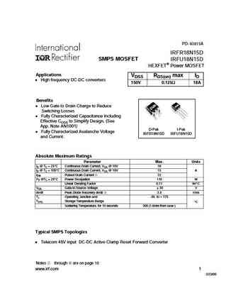
PD- 93815A IRFR18N15D SMPS MOSFET IRFU18N15D HEXFET Power MOSFET Applications VDSS RDS(on) max ID High frequency DC-DC converters 150V 0.125 18A Benefits Low Gate to Drain Charge to Reduce Switching Losses Fully Characterized Capacitance Including Effective COSS to Simplify Design, (See App. Note AN1001) D-Pak I-Pak Fully Characterized Avalanche Voltage IRFR18N15D IRF
irfr18n15dpbf.pdf

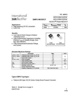
PD - 95061A IRFR18N15DPbF IRFU18N15DPbF SMPS MOSFET HEXFET Power MOSFET Applications VDSS RDS(on) max ID l High frequency DC-DC converters 150V 0.125 18A l Lead-Free Benefits l Low Gate to Drain Charge to Reduce Switching Losses l Fully Characterized Capacitance Including Effective COSS to Simplify Design, (See App. Note AN1001) D-Pak I-Pak l Fully Characterized Avalanche
irfr18n15dpbf irfu18n15dpbf.pdf
PD - 95061A IRFR18N15DPbF IRFU18N15DPbF SMPS MOSFET HEXFET Power MOSFET Applications VDSS RDS(on) max ID l High frequency DC-DC converters 150V 0.125 18A l Lead-Free Benefits l Low Gate to Drain Charge to Reduce Switching Losses l Fully Characterized Capacitance Including Effective COSS to Simplify Design, (See App. Note AN1001) D-Pak I-Pak l Fully Characterized Avalanche
irfr18n15d.pdf
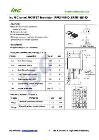
isc N-Channel MOSFET Transistor IRFR18N15D, IIRFR18N15D FEATURES Static drain-source on-resistance RDS(on) 125m Enhancement mode 100% avalanche tested Minimum Lot-to-Lot variations for robust device performance and reliable operation DESCRITION High frequency DC-DC converters ABSOLUTE MAXIMUM RATINGS(T =25 ) a SYMBOL PARAMETER VALUE UNIT V Drain-Source Volt

irfr1205.pdf
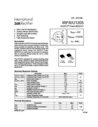
PD - 91318B IRFR/U1205 HEXFET Power MOSFET Ultra Low On-Resistance D Surface Mount (IRFR1205) VDSS = 55V Straight Lead (IRFU1205) Fast Switching RDS(on) = 0.027 Fully Avalanche Rated G Description ID = 44A S Fifth Generation HEXFETs from International Rectifier utilize advanced processing techniques to achieve the lowest possible on-resistance per silicon area. This
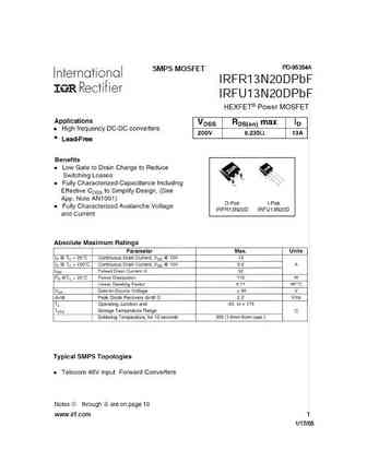
irfr13n15d.pdf
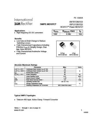
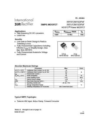
PD - 93905A IRFR13N15D SMPS MOSFET IRFU13N15D HEXFET Power MOSFET Applications VDSS RDS(on) max ID High frequency DC-DC converters 150V 0.18 14A Benefits Low Gate-to-Drain Charge to Reduce Switching Losses Fully Characterized Capacitance Including Effective COSS to Simplify Design, (See App. Note AN1001) Fully Characterized Avalanche Voltage D-Pak I-Pak and Current I
irfr1n60a.pdf
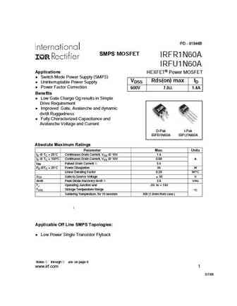
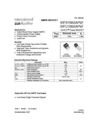
PD - 91846B SMPS MOSFET IRFR1N60A IRFU1N60A Applications HEXFET Power MOSFET l Switch Mode Power Supply (SMPS) VDSS Rds(on) max ID l Uninterruptable Power Supply l Power Factor Correction 600V 7.0 1.4A Benefits l Low Gate Charge Qg results in Simple Drive Requirement l Improved Gate, Avalanche and dynamic dv/dt Ruggedness l Fully Characterized Capacitance and Avalanche Vol
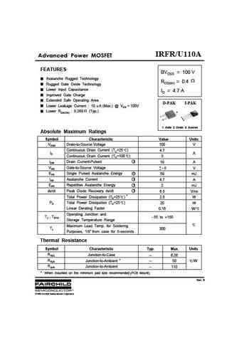
irfr120atm.pdf

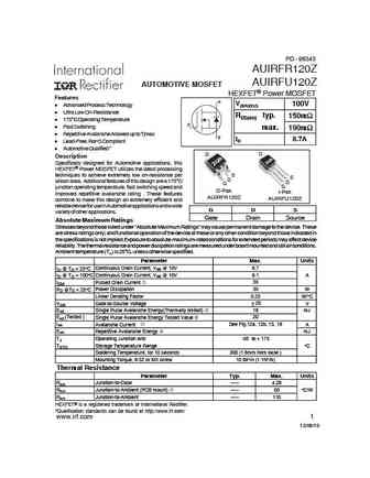
IRFR/U120A Advanced Power MOSFET FEATURES BVDSS = 100 V Avalanche Rugged Technology RDS(on) = 0.2 Rugged Gate Oxide Technology Lower Input Capacitance ID = 8.4 A Improved Gate Charge Extended Safe Operating Area D-PAK I-PAK A (Max.) @ VDS = 100V Lower Leakage Current 10 Lower RDS(ON) 0.155 (Typ.) 2 1 1 2 3 3 1. Gate 2. Drain 3. Source Absolute Maximu
irfr1n60apbf irfu1n60apbf.pdf
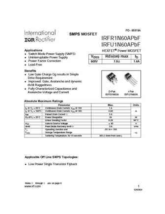
PD - 95518A SMPS MOSFET IRFR1N60APbF IRFU1N60APbF Applications HEXFET Power MOSFET l Switch Mode Power Supply (SMPS) VDSS Rds(on) max ID l Uninterruptable Power Supply l Power Factor Correction 600V 7.0 1.4A l Lead-Free Benefits l Low Gate Charge Qg results in Simple Drive Requirement l Improved Gate, Avalanche and dynamic dv/dt Ruggedness l Fully Characterized Capacitance
irfr1205pbf irfu1205pbf.pdf
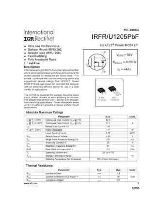
PD - 95600A IRFR/U1205PbF Lead-Free www.irf.com 1 12/9/04 IRFR/U1205PbF 2 www.irf.com IRFR/U1205PbF www.irf.com 3 IRFR/U1205PbF 4 www.irf.com IRFR/U1205PbF www.irf.com 5 IRFR/U1205PbF 6 www.irf.com IRFR/U1205PbF Peak Diode Recovery dv/dt Test Circuit + Circuit Layout Considerations Low Stray Inductance Ground Plane Low Leakage Inductance Current Tr
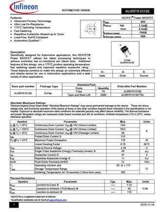
auirfu120z auirfr120z.pdf
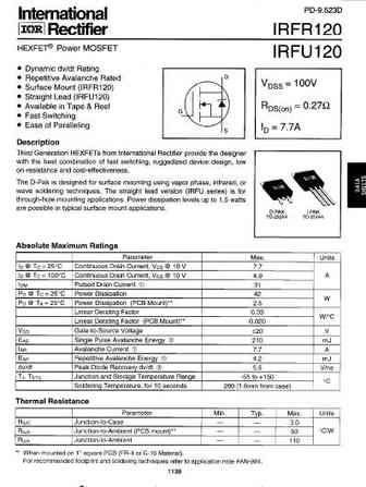
PD - 96345 AUIRFR120Z AUIRFU120Z AUTOMOTIVE MOSFET HEXFET Power MOSFET Features D V(BR)DSS 100V l Advanced Process Technology l Ultra Low On-Resistance RDS(on) typ. 150m l 175 C Operating Temperature G l Fast Switching max. 190m l Repetitive Avalanche Allowed up to Tjmax S ID 8.7A l Lead-Free, RoHS Compliant l Automotive Qualified * D D Description Specificall
irfr1n60apbf irfu1n60apbf.pdf
PD - 95518A SMPS MOSFET IRFR1N60APbF IRFU1N60APbF Applications HEXFET Power MOSFET l Switch Mode Power Supply (SMPS) VDSS Rds(on) max ID l Uninterruptable Power Supply l Power Factor Correction 600V 7.0 1.4A l Lead-Free Benefits l Low Gate Charge Qg results in Simple Drive Requirement l Improved Gate, Avalanche and dynamic dv/dt Ruggedness l Fully Characterized Capacitance
irfr13n15dpbf irfr13n15dpbf.pdf

PD - 95549A IRFR13N15DPbF IRFU13N15DPbF SMPS MOSFET HEXFET Power MOSFET Applications VDSS RDS(on) max ID l High frequency DC-DC converters 150V 0.18 14A l Lead-Free Benefits l Low Gate-to-Drain Charge to Reduce Switching Losses l Fully Characterized Capacitance Including Effective COSS to Simplify Design, (See App. Note AN1001) l Fully Characterized Avalanche Voltage D-Pa
irfu13n15dpbf irfr13n15dpbf.pdf

PD - 95549A IRFR13N15DPbF IRFU13N15DPbF SMPS MOSFET HEXFET Power MOSFET Applications VDSS RDS(on) max ID l High frequency DC-DC converters 150V 0.18 14A l Lead-Free Benefits l Low Gate-to-Drain Charge to Reduce Switching Losses l Fully Characterized Capacitance Including Effective COSS to Simplify Design, (See App. Note AN1001) l Fully Characterized Avalanche Voltage D-Pa
irfr13n20d.pdf
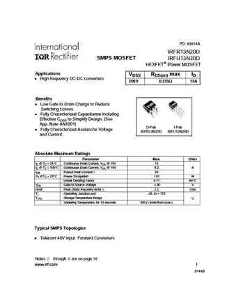
PD- 93814A IRFR13N20D SMPS MOSFET IRFU13N20D HEXFET Power MOSFET Applications VDSS RDS(on) max ID High frequency DC-DC converters 200V 0.235 13A Benefits Low Gate to Drain Charge to Reduce Switching Losses Fully Characterized Capacitance Including Effective COSS to Simplify Design, (See App. Note AN1001) D-Pak I-Pak Fully Characterized Avalanche Voltage IRFR13N20D IRF
irfr1010zpbf irfu1010zpbf.pdf
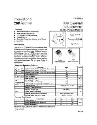
PD - 95951A IRFR1010ZPbF IRFU1010ZPbF Features HEXFET Power MOSFET Advanced Process Technology D Ultra Low On-Resistance VDSS = 55V 175 C Operating Temperature Fast Switching Repetitive Avalanche Allowed up to Tjmax RDS(on) = 7.5m G Lead-Free ID = 42A Description S This HEXFET Power MOSFET utilizes the latest processing techniques to achieve extremely low on-re
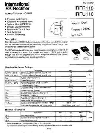
irfr110pbf irfu110pbf.pdf
PD - 95026A IRFR110PbF IRFU110PbF Lead-Free 12/14/04 Document Number 91265 www.vishay.com 1 IRFR/U110PbF Document Number 91265 www.vishay.com 2 IRFR/U110PbF Document Number 91265 www.vishay.com 3 IRFR/U110PbF Document Number 91265 www.vishay.com 4 IRFR/U110PbF Document Number 91265 www.vishay.com 5 IRFR/U110PbF Document Number 91265 www.vishay.com 6 IRFR/U1
irfr120npbf irfu120npbf.pdf
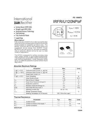
PD - 95067A IRFR/U120NPbF Lead-Free www.irf.com 1 12/9/04 IRFR/U120NPbF 2 www.irf.com IRFR/U120NPbF www.irf.com 3 IRFR/U120NPbF 4 www.irf.com IRFR/U120NPbF www.irf.com 5 IRFR/U120NPbF 6 www.irf.com IRFR/U120NPbF www.irf.com 7 IRFR/U120NPbF D-Pak (TO-252AA) Package Outline Dimensions are shown in millimeters (inches) D-Pak (TO-252AA) Part Marking Information EXAMP
irfr120zpbf irfu120zpbf.pdf
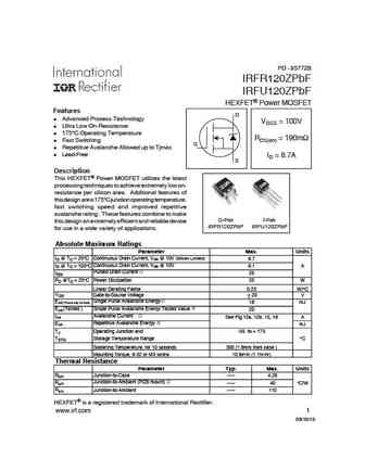
PD - 95772B IRFR120ZPbF IRFU120ZPbF HEXFET Power MOSFET Features D Advanced Process Technology VDSS = 100V Ultra Low On-Resistance 175 C Operating Temperature RDS(on) = 190m Fast Switching G Repetitive Avalanche Allowed up to Tjmax Lead-Free ID = 8.7A S Description This HEXFET Power MOSFET utilizes the latest processing techniques to achieve extremely low on- r
irfr1018epbf irfu1018epbf.pdf
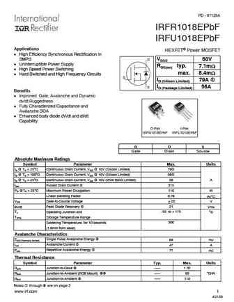
PD - 97129A IRFR1018EPbF IRFU1018EPbF Applications HEXFET Power MOSFET l High Efficiency Synchronous Rectification in SMPS D VDSS 60V l Uninterruptible Power Supply RDS(on) typ. 7.1m l High Speed Power Switching max. 8.4m l Hard Switched and High Frequency Circuits G ID (Silicon Limited) 79A c ID (Package Limited) S 56A Benefits l Improved Gate, Avalanche and Dyna
irfr12n25dpbf irfu12n25dpbf.pdf
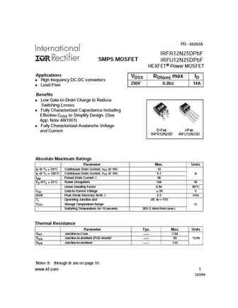
PD - 95353A IRFR12N25DPbF SMPS MOSFET IRFU12N25DPbF HEXFET Power MOSFET Applications VDSS RDS(on) max ID l High frequency DC-DC converters 250V 0.26 14A l Lead-Free Benefits l Low Gate-to-Drain Charge to Reduce Switching Losses l Fully Characterized Capacitance Including Effective COSS to Simplify Design, (See App. Note AN1001) l Fully Characterized Avalanche Voltage D-Pa
auirfr1010z.pdf
PD - 97683 AUTOMOTIVE GRADE AUIRFR1010Z HEXFET Power MOSFET Features D VDSS Advanced Process Technology 55V Low On-Resistance RDS(on) typ. 5.8m 175 C Operating Temperature max. 7.5m G Fast Switching ID (Silicon Limited) 91A Repetitive Avalanche Allowed up to Tjmax ID (Package Limited) S 42A Lead-Free, RoHS Compliant Automotive Qualifie
irfr12n25d.pdf
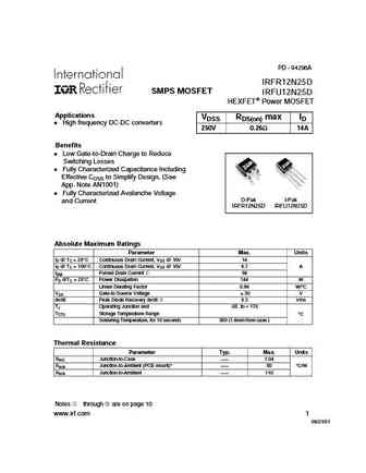
PD - 94296A IRFR12N25D SMPS MOSFET IRFU12N25D HEXFET Power MOSFET Applications VDSS RDS(on) max ID High frequency DC-DC converters 250V 0.26 14A Benefits Low Gate-to-Drain Charge to Reduce Switching Losses Fully Characterized Capacitance Including Effective COSS to Simplify Design, (See App. Note AN1001) Fully Characterized Avalanche Voltage D-Pak I-Pak and Current I
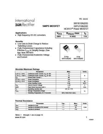
irfr15n20dpbf irfu15n20dpbf.pdf
PD - 95355A IRFR15N20DPbF SMPS MOSFET IRFU15N20DPbF HEXFET Power MOSFET Applications VDSS RDS(on) max ID l High frequency DC-DC converters 200V 0.165 17A l Lead-Free Benefits l Low Gate-to-Drain Charge to Reduce Switching Losses l Fully Characterized Capacitance Including Effective COSS to Simplify Design, (See App. Note AN1001) l Fully Characterized Avalanche Voltage D-P
irfr120n.pdf

PD - 91365B IRFR/U120N HEXFET Power MOSFET Surface Mount (IRFR120N) D Straight Lead (IRFU120N) VDSS = 100V Advanced Process Technology Fast Switching RDS(on) = 0.21 Fully Avalanche Rated G Description ID = 9.4A S Fifth Generation HEXFETs from International Rectifier utilize advanced processing techniques to achieve the lowest possible on-resistance per silicon area. T
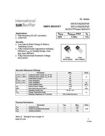
irfr15n20d.pdf
PD - 94245 IRFR15N20D SMPS MOSFET IRFU15N20D HEXFET Power MOSFET Applications VDSS RDS(on) max ID High frequency DC-DC converters 200V 0.165 17A Benefits Low Gate-to-Drain Charge to Reduce Switching Losses Fully Characterized Capacitance Including Effective COSS to Simplify Design, (See App. Note AN1001) Fully Characterized Avalanche Voltage D-Pak I-Pak and Current I
irfr13n20dpbf irfu13n20dpbf.pdf
PD-95354A SMPS MOSFET IRFR13N20DPbF IRFU13N20DPbF Lead-Free www.irf.com 1 1/17/05 IRFR/U13N20DPbF 2 www.irf.com IRFR/U13N20DPbF www.irf.com 3 IRFR/U13N20DPbF 4 www.irf.com IRFR/U13N20DPbF www.irf.com 5 IRFR/U13N20DPbF 6 www.irf.com IRFR/U13N20DPbF www.irf.com 7 IRFR/U13N20DPbF D-Pak (TO-252AA) Package Outline Dimensions are shown in millimeters (inches) D-Pak (T
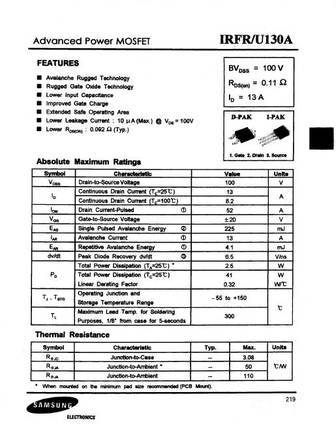
irfr130atm.pdf

IRFR/U130A Advanced Power MOSFET FEATURES BVDSS = 100 V Avalanche Rugged Technology RDS(on) = 0.11 Rugged Gate Oxide Technology Lower Input Capacitance ID = 13 A Improved Gate Charge Extended Safe Operating Area D-PAK I-PAK Lower Leakage Current 10 A (Max.) @ VDS = 100V (Typ.) Lower RDS(ON) 0.092 2 1 1 2 3 3 1. Gate 2. Drain 3. Source Absolute Maximum
auirfr120ztrl.pdf

PD - 96345 AUIRFR120Z AUIRFU120Z AUTOMOTIVE MOSFET HEXFET Power MOSFET Features D V(BR)DSS 100V l Advanced Process Technology l Ultra Low On-Resistance RDS(on) typ. 150m l 175 C Operating Temperature G l Fast Switching max. 190m l Repetitive Avalanche Allowed up to Tjmax S ID 8.7A l Lead-Free, RoHS Compliant l Automotive Qualified * D D Description Specificall
irfr120pbf irfu120pbf.pdf
PD- 95523A IRFR120PbF IRFU120PbF Lead-Free 12/03/04 Document Number 91266 www.vishay.com 1 IRFR/U120PbF Document Number 91266 www.vishay.com 2 IRFR/U120PbF Document Number 91266 www.vishay.com 3 IRFR/U120PbF Document Number 91266 www.vishay.com 4 IRFR/U120PbF Document Number 91266 www.vishay.com 5 IRFR/U120PbF Document Number 91266 www.vishay.com 6 IRFR/U12
irfr13n15dpbf.pdf
PD - 95549A IRFR13N15DPbF IRFU13N15DPbF SMPS MOSFET HEXFET Power MOSFET Applications VDSS RDS(on) max ID l High frequency DC-DC converters 150V 0.18 14A l Lead-Free Benefits l Low Gate-to-Drain Charge to Reduce Switching Losses l Fully Characterized Capacitance Including Effective COSS to Simplify Design, (See App. Note AN1001) l Fully Characterized Avalanche Voltage D-Pa
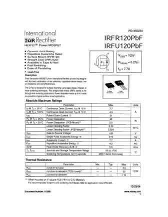
irfr120a irfu120a.pdf

IRFR/U120A Advanced Power MOSFET FEATURES BVDSS = 100 V Avalanche Rugged Technology RDS(on) = 0.2 Rugged Gate Oxide Technology Lower Input Capacitance ID = 8.4 A Improved Gate Charge Extended Safe Operating Area D-PAK I-PAK A (Max.) @ VDS = 100V Lower Leakage Current 10 Lower RDS(ON) 0.155 (Typ.) 2 1 1 2 3 3 1. Gate 2. Drain 3. Source Absolute Maximu
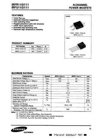
irfr110a irfu110a.pdf
IRFR/U110A Advanced Power MOSFET FEATURES BVDSS = 100 V Avalanche Rugged Technology RDS(on) = 0.4 Rugged Gate Oxide Technology Lower Input Capacitance ID = 4.7 A Improved Gate Charge Extended Safe Operating Area D-PAK I-PAK Lower Leakage Current 10 A (Max.) @ VDS = 100V Lower RDS(ON) 0.289 (Typ.) 2 1 1 2 3 3 1. Gate 2. Drain 3. Source Absolute Maxim
irfr110a.pdf
Advanced Power MOSFET FEATURES BVDSS = 100 V Avalanche Rugged Technology RDS(on) = 0.4 Rugged Gate Oxide Technology Lower Input Capacitance ID = 4.7 A Improved Gate Charge Extended Safe Operating Area Lower Leakage Current 10 A (Max.) @ VDS = 100V Lower RDS(ON) 0.289 (Typ.) 2 1 1 2 3 3 1. Gate 2. Drain 3. Source Absolute Maximum Ratings Symbol Charact
irfr120a.pdf
Advanced Power MOSFET FEATURES BVDSS = 100 V Avalanche Rugged Technology RDS(on) = 0.2 Rugged Gate Oxide Technology Lower Input Capacitance ID = 8.4 A Improved Gate Charge Extended Safe Operating Area Lower Leakage Current 10 A (Max.) @ VDS = 100V Lower RDS(ON) 0.155 (Typ.) 2 1 1 2 3 3 1. Gate 2. Drain 3. Source Absolute Maximum Ratings Symbol Chara
irfr130a.pdf

Advanced Power MOSFET FEATURES BVDSS = 100 V Avalanche Rugged Technology RDS(on) = 0.11 Rugged Gate Oxide Technology Lower Input Capacitance ID = 13 A Improved Gate Charge Extended Safe Operating Area Lower Leakage Current 10 A (Max.) @ VDS = 100V Lower RDS(ON) 0.092 2 (Typ.) 1 1 2 3 3 1. Gate 2. Drain 3. Source Absolute Maximum Ratings Symbol C
irfr120pbf irfu120pbf sihfr120 sihfu120.pdf

IRFR120, IRFU120, SiHFR120, SiHFU120 Vishay Siliconix Power MOSFET FEATURES PRODUCT SUMMARY Halogen-free According to IEC 61249-2-21 VDS (V) 100 Definition Dynamic dV/dt Rating RDS(on) ( )VGS = 10 V 0.27 Repetitive Avalanche Rated Qg (Max.) (nC) 16 Surface Mount (IRFR120, SiHFR120) Qgs (nC) 4.4 Straight Lead (IRFU120, SiHFU120) Available in Tape and Reel Q
irfr110 sihfr110.pdf
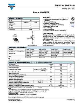
IRFR110, SiHFR110 Vishay Siliconix Power MOSFET FEATURES PRODUCT SUMMARY Halogen-free According to IEC 61249-2-21 VDS (V) 100 Definition Dynamic dV/dt Rating RDS(on) ( )VGS = 10 V 0.54 Repetitive Avalanche Rated Qg (Max.) (nC) 8.3 Surface Mount (IRFR110, SiHFR110) Qgs (nC) 2.3 Available in Tape and Reel Qgd (nC) 3.8 Fast Switching Configuration Single
irfr1n60a irfu1n60a sihfr1n60a sihfu1n60a.pdf
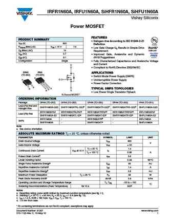
IRFR1N60A, IRFU1N60A, SiHFR1N60A, SiHFU1N60A Vishay Siliconix Power MOSFET FEATURES PRODUCT SUMMARY Halogen-free According to IEC 61249-2-21 VDS (V) 600 Definition RDS(on) (Max.) ( )VGS = 10 V 7.0 Low Gate Charge Qg Results in Simple Drive Qg (Max.) (nC) 14 Requirement Qgs (nC) 2.7 Improved Gate, Avalanche and Dynamic Qgd (nC) 8.1 dV/dt Ruggedness Configuration Sing
irfr120 irfu120 sihfr120 sihfu120.pdf
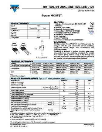
IRFR120, IRFU120, SiHFR120, SiHFU120 Vishay Siliconix Power MOSFET FEATURES PRODUCT SUMMARY Halogen-free According to IEC 61249-2-21 VDS (V) 100 Definition Dynamic dV/dt Rating RDS(on) ( )VGS = 10 V 0.27 Repetitive Avalanche Rated Qg (Max.) (nC) 16 Surface Mount (IRFR120, SiHFR120) Qgs (nC) 4.4 Straight Lead (IRFU120, SiHFU120) Available in Tape and Reel Q
irfr110pbf sihfr110.pdf

IRFR110, SiHFR110 Vishay Siliconix Power MOSFET FEATURES PRODUCT SUMMARY Halogen-free According to IEC 61249-2-21 VDS (V) 100 Definition Dynamic dV/dt Rating RDS(on) ( )VGS = 10 V 0.54 Repetitive Avalanche Rated Qg (Max.) (nC) 8.3 Surface Mount (IRFR110, SiHFR110) Qgs (nC) 2.3 Available in Tape and Reel Qgd (nC) 3.8 Fast Switching Configuration Single
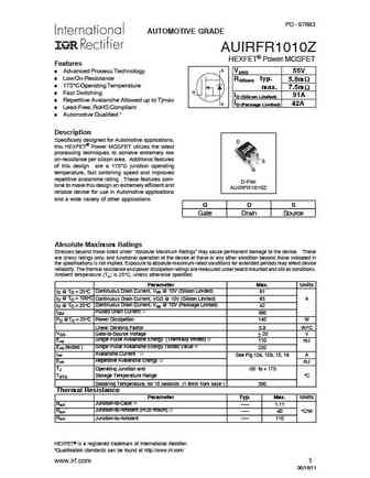
auirfr1018e.pdf
AUTOMOTIVE GRADE AUIRFR1018E Features HEXFET Power MOSFET Advanced Process Technology VDSS 60V Ultra Low On-Resistance RDS(on) typ. 7.1m 175 C Operating Temperature max. 8.4m Fast Switching ID (Silicon Limited) 79A Repetitive Avalanche Allowed up to Tjmax ID (Package Limited) 56A Lead-Free, RoHS Compliant Automotive Qu
irfr1205.pdf
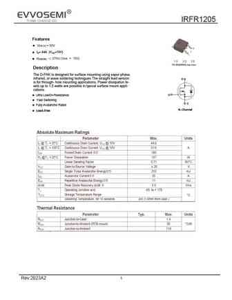
IRFR1205 Features l VDS (V) = 55V ID= 44A (VGS=10V) l 27m (VGS = 10V) l l RDS(ON) Description The D-PAK is designed for surface mounting using vapor phase, infrared, or wave soldering technigues The straight lead version D is for through- hole mounting applications. Power dissipation le- vels up to 1.5 watts are possible in typical surface mount appli- cations. G l Ultra LowOn
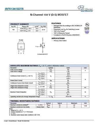
irfr15n20dtr.pdf
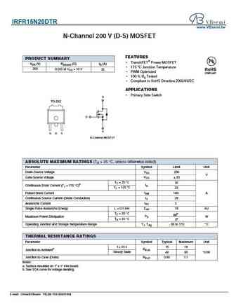
IRFR15N20DTR www.VBsemi.tw N-Channel 200 V (D-S) MOSFET FEATURES PRODUCT SUMMARY TrenchFET Power MOSFET VDS (V) RDS(on) ( )ID (A) 175 C Junction Temperature 200 0.055 at VGS = 10 V 30 PWM Optimized 100 % Rg Tested Compliant to RoHS Directive 2002/95/EC APPLICATIONS Primary Side Switch D TO-252 G S G D S N-Channel MOSFET ABSOLUTE MAXIMUM RA
irfr13n20dtr.pdf
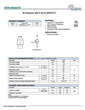
IRFR13N20DTR www.VBsemi.tw N-Channel 200 V (D-S) MOSFET FEATURES PRODUCT SUMMARY TrenchFET Power MOSFET VDS (V) RDS(on) ( )ID (A) 175 C Junction Temperature 200 0.055 at VGS = 10 V 30 PWM Optimized 100 % Rg Tested Compliant to RoHS Directive 2002/95/EC APPLICATIONS Primary Side Switch D TO-252 G S G D S N-Channel MOSFET ABSOLUTE MAXIMUM RA
irfr13n15dtr.pdf
IRFR13N15DTR www.VBsemi.tw N-Channel 150 V (D-S) MOSFET FEATURES PRODUCT SUMMARY Halogen-free According to IEC 61249-2-21 VDS (V) RDS(on) ( )ID (A)a Qg (Typ.) Definition 0.074 at VGS = 10 V 25.4 Extremely Low Qgd for Switching Losses 150 23 nC 0.077 at VGS = 8 V 22.5 100 % Rg Tested 100 % Avalanche Tested Compliant to RoHS Directive 2002/95/EC D APPLICATION
irfr120tr.pdf

IRFR120TR www.VBsemi.tw N-Channel 100 V (D-S) MOSFET FEATURES PRODUCT SUMMARY TrenchFET Power MOSFET VDS (V) RDS(on) ( )ID (A) 175 C Junction Temperature 100 0.11 4 at VGS = 10 V 15 PWM Optimized 100 % Rg Tested Compliant to RoHS Directive 2002/95/EC APPLICATIONS Primary Side Switch D TO-252 G S G D S N-Channel MOSFET ABSOLUTE MAXIMUM RATINGS
irfr120ntrpbf.pdf
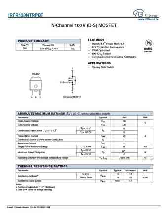
IRFR120NTRPBF www.VBsemi.tw N-Channel 100 V (D-S) MOSFET FEATURES PRODUCT SUMMARY TrenchFET Power MOSFET VDS (V) RDS(on) ( )ID (A) 175 C Junction Temperature 100 0.11 4 at VGS = 10 V 15 PWM Optimized 100 % Rg Tested Compliant to RoHS Directive 2002/95/EC APPLICATIONS Primary Side Switch D TO-252 G S G D S N-Channel MOSFET ABSOLUTE MAXIMUM RAT
irfr110tr.pdf
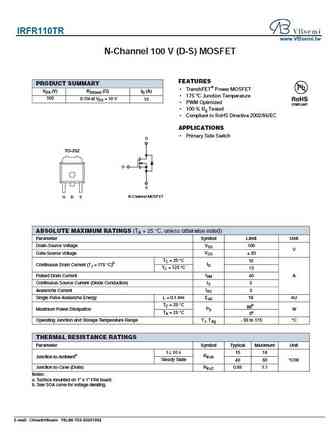
IRFR110TR www.VBsemi.tw N-Channel 100 V (D-S) MOSFET FEATURES PRODUCT SUMMARY TrenchFET Power MOSFET VDS (V) RDS(on) ( )ID (A) 175 C Junction Temperature 100 0.11 4 at VGS = 10 V 15 PWM Optimized 100 % Rg Tested Compliant to RoHS Directive 2002/95/EC APPLICATIONS Primary Side Switch D TO-252 G S G D S N-Channel MOSFET ABSOLUTE MAXIMUM RATINGS
irfr130atm.pdf
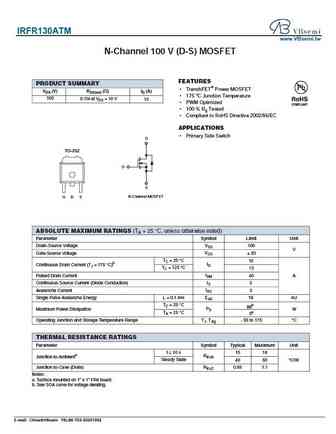
IRFR130ATM www.VBsemi.tw N-Channel 100 V (D-S) MOSFET FEATURES PRODUCT SUMMARY TrenchFET Power MOSFET VDS (V) RDS(on) ( )ID (A) 175 C Junction Temperature 100 0.11 4 at VGS = 10 V 15 PWM Optimized 100 % Rg Tested Compliant to RoHS Directive 2002/95/EC APPLICATIONS Primary Side Switch D TO-252 G S G D S N-Channel MOSFET ABSOLUTE MAXIMUM RATING
irfr1205tr.pdf
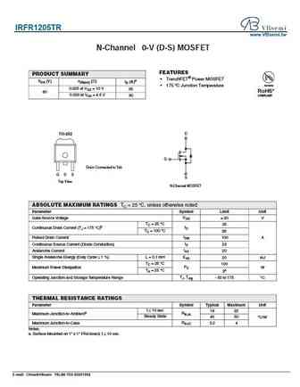
IRFR1205TR www.VBsemi.tw N-Channel 6 0-V (D-S) MOSFET FEATURES PRODUCT SUMMARY TrenchFET Power MOSFET VDS (V) rDS(on) ( ) ID (A)a Available 175 C Junction Temperature 0.025 at VGS = 10 V 35 RoHS* 60 0.030 at VGS = 4.5 V 30 COMPLIANT TO-252 D G Drain Connected to Tab G D S S Top View N-Channel MOSFET ABSOLUTE MAXIMUM RATINGS TC = 25 C, unless otherwise no
irfr1205tr.pdf
60V N-Channel Power MOSFET DESCRIPTION The IRFR1205TR uses advanced trench technology to provide excellent RDS(ON), low gate charge. It can be used in a wide variety of applications. KEY CHARACTERISTICS VDS = 60V,ID= 30A Schematic diagram RDS(ON)
irfr1205.pdf
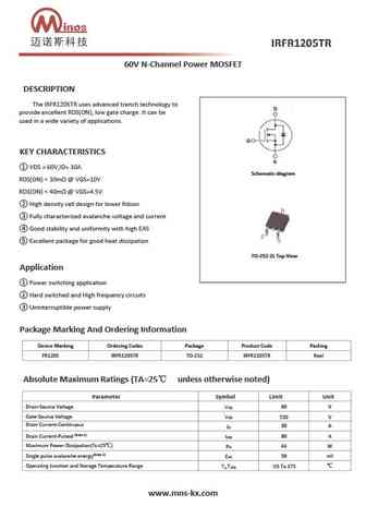
isc N-Channel MOSFET Transistor IRFR1205, IIRFR1205 FEATURES Static drain-source on-resistance RDS(on) 27m Enhancement mode 100% avalanche tested Minimum Lot-to-Lot variations for robust device performance and reliable operation DESCRITION Fast Switching ABSOLUTE MAXIMUM RATINGS(T =25 ) a SYMBOL PARAMETER VALUE UNIT V Drain-Source Voltage 55 V DSS V Gate-
irfr13n15d.pdf

isc N-Channel MOSFET Transistor IRFR13N15D, IIRFR13N15D FEATURES Static drain-source on-resistance RDS(on) 180m Enhancement mode 100% avalanche tested Minimum Lot-to-Lot variations for robust device performance and reliable operation DESCRITION High frequency DC-DC converters ABSOLUTE MAXIMUM RATINGS(T =25 ) a SYMBOL PARAMETER VALUE UNIT V Drain-Source Volt
irfr1n60a.pdf
iscN-Channel MOSFET Transistor IRFR1N60A FEATURES Low drain-source on-resistance RDS(ON) =7 (MAX) Enhancement mode Vth = 2.0 to 4.0V (VDS = 10 V, ID=0.25mA) 100% avalanche tested Minimum Lot-to-Lot variations for robust device performance and reliable operation DESCRITION Switching Voltage Regulators ABSOLUTE MAXIMUM RATINGS(T =25 ) a SYMBOL PARAMETER VALUE U
irfr1018e.pdf
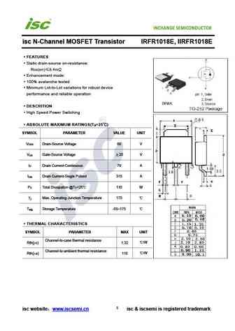
isc N-Channel MOSFET Transistor IRFR1018E, IIRFR1018E FEATURES Static drain-source on-resistance RDS(on) 8.4m Enhancement mode 100% avalanche tested Minimum Lot-to-Lot variations for robust device performance and reliable operation DESCRITION High Speed Power Switching ABSOLUTE MAXIMUM RATINGS(T =25 ) a SYMBOL PARAMETER VALUE UNIT V Drain-Source Voltage 60
irfr13n20d.pdf

isc N-Channel MOSFET Transistor IRFR13N20D, IIRFR13N20D FEATURES Static drain-source on-resistance RDS(on) 235m Enhancement mode 100% avalanche tested Minimum Lot-to-Lot variations for robust device performance and reliable operation DESCRITION High frequency DC-DC converters ABSOLUTE MAXIMUM RATINGS(T =25 ) a SYMBOL PARAMETER VALUE UNIT V Drain-Source Volt
irfr120z.pdf

isc N-Channel MOSFET Transistor IRFR120Z, IIRFR120Z FEATURES Static drain-source on-resistance RDS(on) 190m Enhancement mode 100% avalanche tested Minimum Lot-to-Lot variations for robust device performance and reliable operation DESCRITION Fast switching ABSOLUTE MAXIMUM RATINGS(T =25 ) a SYMBOL PARAMETER VALUE UNIT V Drain-Source Voltage 100 V DSS V Gat
irfr1010z.pdf

isc N-Channel MOSFET Transistor IRFR1010Z, IIRFR1010Z FEATURES Static drain-source on-resistance RDS(on) 7.5m Enhancement mode 100% avalanche tested Minimum Lot-to-Lot variations for robust device performance and reliable operation DESCRITION Fast switching ABSOLUTE MAXIMUM RATINGS(T =25 ) a SYMBOL PARAMETER VALUE UNIT V Drain-Source Voltage 55 V DSS V Ga
irfr120n.pdf
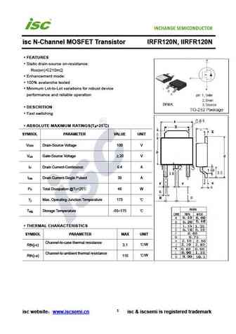
isc N-Channel MOSFET Transistor IRFR120N, IIRFR120N FEATURES Static drain-source on-resistance RDS(on) 210m Enhancement mode 100% avalanche tested Minimum Lot-to-Lot variations for robust device performance and reliable operation DESCRITION Fast switching ABSOLUTE MAXIMUM RATINGS(T =25 ) a SYMBOL PARAMETER VALUE UNIT V Drain-Source Voltage 100 V DSS V Gat
irfr15n20d.pdf

isc N-Channel MOSFET Transistor IRFR15N20D, IIRFR15N20D FEATURES Static drain-source on-resistance RDS(on) 165m Enhancement mode 100% avalanche tested Minimum Lot-to-Lot variations for robust device performance and reliable operation DESCRITION High frequency DC-DC converters ABSOLUTE MAXIMUM RATINGS(T =25 ) a SYMBOL PARAMETER VALUE UNIT V Drain-Source Volt
Otros transistores... IRFPS3810 , IRFPS3815 , IRFR1010Z , IRFR1018E , IRFR120Z , IRFR13N15D , IRFR13N20D , IRFR15N20D , 2N7002 , IRFR220N , IRFR2307Z , IRFR2405 , IRFR2407 , IRFR24N15D , IRFR2607Z , IRFR2905Z , IRFR3410 .
History: BS170P | BFR30 | BS250P | BSN254A | CHM4311PAGP | BSP92
History: BS170P | BFR30 | BS250P | BSN254A | CHM4311PAGP | BSP92
🌐 : EN ES РУ

Liste
Recientemente añadidas las descripciónes de los transistores:
MOSFET: ASB80R750E | ASB70R380E | ASB65R300E | ASB65R220E | ASB65R120EFD | ASB60R150E | ASA80R900E | ASA80R750E | ASA80R290E | ASA70R950E | ASA70R600E | ASA70R380E | ASA70R240E | ASA65R850E | ASA65R550E | ASA65R350E
Popular searches
13009 transistor | irf3205 equivalent | ksa992 transistor | 2n2926 | ksa992 pinout | 2n1308 transistor | p609 | bc327-40