SSM3J36FS MOSFET Equivalente. Reemplazo. Hoja de especificaciones. Principales características
Número de Parte: SSM3J36FS
Tipo de FET: MOSFET
Polaridad de transistor: P
ESPECIFICACIONES MÁXIMAS
Pdⓘ - Máxima
disipación de potencia: 0.15 W
|Vds|ⓘ - Voltaje máximo drenador-fuente: 20 V
|Vgs|ⓘ - Voltaje máximo fuente-puerta: 8 V
|Id|ⓘ - Corriente continua
de drenaje: 0.33 A
Tjⓘ - Temperatura máxima de unión: 150 °C
CARACTERÍSTICAS ELÉCTRICAS
Cossⓘ - Capacitancia de salida: 10.3 pF
RDSonⓘ - Resistencia estado encendido drenaje a fuente: 1.31 Ohm
Encapsulados: SOT416
SC75
SSM
Búsqueda de reemplazo de SSM3J36FS MOSFET
- Selecciónⓘ de transistores por parámetros
SSM3J36FS datasheet
..1. Size:184K toshiba
ssm3j36fs.pdf 
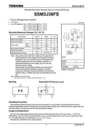
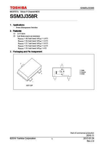
SSM3J36FS TOSHIBA Field Effect Transistor Silicon P Channel MOS Type SSM3J36FS Power Management Switches 1.5-V drive Unit mm Low ON-resistance Ron = 3.60 (max) (@VGS = -1.5 V) Ron = 2.70 (max) (@VGS = -1.8 V) Ron = 1.60 (max) (@VGS = -2.8 V) Ron = 1.31 (max) (@VGS = -4.5 V) Absolute Maximum Ratings (Ta = 25 C) Characteristics Symbol Rating
..2. Size:784K cn vbsemi
ssm3j36fs.pdf
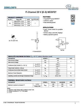
SSM3J36FS www.VBsemi.tw P-Channel 20 V (D-S) MOSFET FEATURES PRODUCT SUMMARY TrenchFET power MOSFET VDS (V) RDS(on) ( )ID (A) Qg (TYP.) (nC) 100 % R tested 0.450 at VGS = -4.5 V -0.55 Fast switching speed -20 0.500 at VGS = -2.5 V -0.50 1 0.600 at VGS = -1.8 V -0.38 APPLICATIONS Load / power switch for portable devices S Drivers relays, solenoids, display
7.1. Size:161K toshiba
ssm3j36mfv.pdf
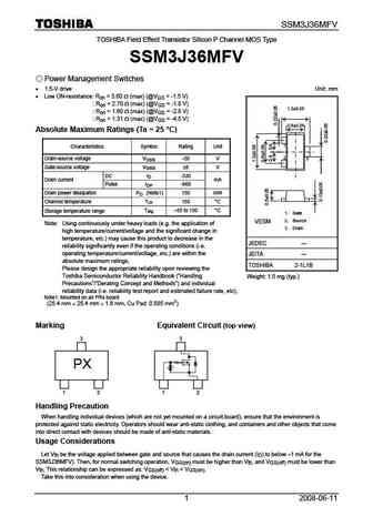
SSM3J36MFV TOSHIBA Field Effect Transistor Silicon P Channel MOS Type SSM3J36MFV Power Management Switches 1.5-V drive Unit mm Low ON-resistance Ron = 3.60 (max) (@VGS = -1.5 V) Ron = 2.70 (max) (@VGS = -1.8 V) 1.2 0.05 Ron = 1.60 (max) (@VGS = -2.8 V) Ron = 1.31 (max) (@VGS = -4.5 V) 0.8 0.05 Absolute Maximum Ratings (Ta = 25 C) 1 Ch
7.2. Size:180K toshiba
ssm3j36tu.pdf
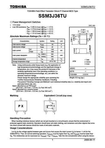
SSM3J36TU TOSHIBA Field Effect Transistor Silicon P Channel MOS Type SSM3J36TU Power Management Switches 1.5-V drive Unit mm Low ON-resistance Ron = 3.60 (max) (@VGS = -1.5 V) Ron = 2.70 (max) (@VGS = -1.8 V) 2.1 0.1 Ron = 1.60 (max) (@VGS = -2.8 V) 1.7 0.1 Ron = 1.31 (max) (@VGS = -4.5 V) Absolute Maximum Ratings (Ta = 25 C) 1 3 2
8.2. Size:254K toshiba
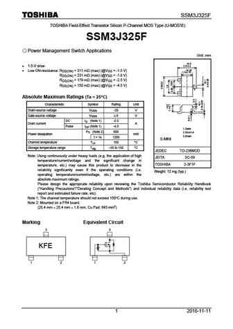
ssm3j325f.pdf
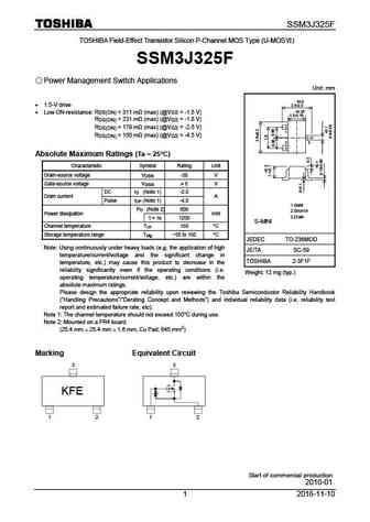
SSM3J325F TOSHIBA Field-Effect Transistor Silicon P-Channel MOS Type (U-MOS ) SSM3J325F Power Management Switch Applications Unit mm +0.5 1.5-V drive 2.5-0.3 +0.25 Low ON-resistance R = 311 m (max) (@V = -1.5 V) DS(ON) GS 1.5-0.15 R = 231 m (max) (@V = -1.8 V) DS(ON) GS R = 179 m (max) (@V = -2.5 V) DS(ON) GS 1 R = 150 m (max) (@V = -4.5 V)
8.3. Size:224K toshiba
ssm3j356r.pdf
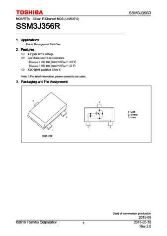
SSM3J356R MOSFETs Silicon P-Channel MOS (U-MOS ) SSM3J356R SSM3J356R SSM3J356R SSM3J356R 1. Applications 1. Applications 1. Applications 1. Applications Power Management Switches 2. Features 2. Features 2. Features 2. Features (1) 4 V gate drive voltage. (2) Low drain-source on-resistance RDS(ON) = 400 m (max) (@VGS = -4.0 V) RDS(ON) = 300 m (max) (@VGS = -10 V)
8.4. Size:173K toshiba
ssm3j306t.pdf
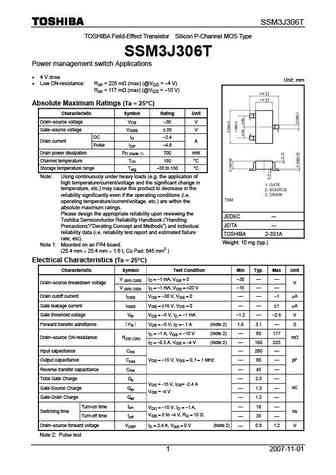
SSM3J306T TOSHIBA Field-Effect Transistor Silicon P-Channel MOS Type SSM3J306T Power management switch Applications 4 V drive Unit mm Low ON-resistance Ron = 225 m (max) (@VGS = -4 V) Ron = 117 m (max) (@VGS = -10 V) Absolute Maximum Ratings (Ta = 25 C) Characteristic Symbol Rating Unit Drain source voltage VDS -30 V Gate source voltage VGSS 20 V DC
8.6. Size:177K toshiba
ssm3j312t.pdf
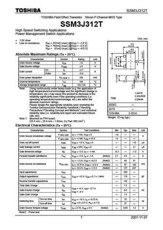
SSM3J312T TOSHIBA Field Effect Transistor Silicon P-Channel MOS Type SSM3J312T High Speed Switching Applications Power Management Switch Applications Unit mm 1.8V drive Low on-resistance Ron = 237m (max) (@VGS = -1.8 V) +0.2 Ron = 142m (max) (@VGS = -2.5 V) 2.8-0.3 Ron = 91m (max) (@VGS = -4.0 V) +0.2 1.6-0.1 Absolute Maximum Ratings (Ta = 25 C) Charac
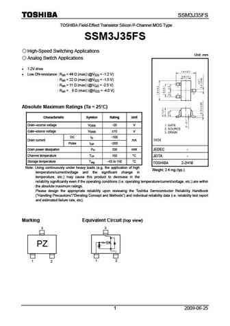
8.8. Size:247K toshiba
ssm3j35mfv.pdf
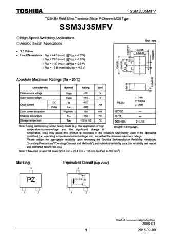
SSM3J35MFV TOSHIBA Field-Effect Transistor Silicon P-Channel MOS Type SSM3J35MFV High-Speed Switching Applications Unit mm Analog Switch Applications 1.2 0.05 1.2 V drive 0.8 0.05 Low ON-resistance R = 44 (max) (@V = -1.2 V) on GS R = 22 (max) (@V = -1.5 V) on GS 1 R = 11 (max) (@V = -2.5 V) on GS R = 8 (max) (@V = -4.0 V) o
8.9. Size:207K toshiba
ssm3j307t.pdf
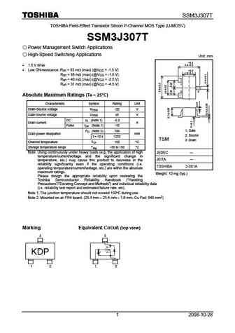
SSM3J307T TOSHIBA Field-Effect Transistor Silicon P-Channel MOS Type (U-MOSV) SSM3J307T Power Management Switch Applications High-Speed Switching Applications Unit mm +0.2 1.5 V drive 2.8-0.3 Low ON-resistance Ron = 83 m (max) (@VGS = -1.5 V) +0.2 1.6-0.1 Ron = 56 m (max) (@VGS = -1.8 V) Ron = 40 m (max) (@VGS = -2.5 V) Ron = 31 m (max) (@VGS = -4.
8.10. Size:350K toshiba
ssm3j338r.pdf
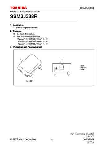
SSM3J338R MOSFETs Silicon P-Channel MOS SSM3J338R SSM3J338R SSM3J338R SSM3J338R 1. Applications 1. Applications 1. Applications 1. Applications Power Management Switches 2. Features 2. Features 2. Features 2. Features (1) 1.8 V gate drive voltage. (2) Low drain-source on-resistance RDS(ON) = 26.3 m (typ.) (@VGS = -1.8 V) RDS(ON) = 20.1 m (typ.) (@VGS = -2.5 V) R
8.11. Size:468K toshiba
ssm3j334r.pdf
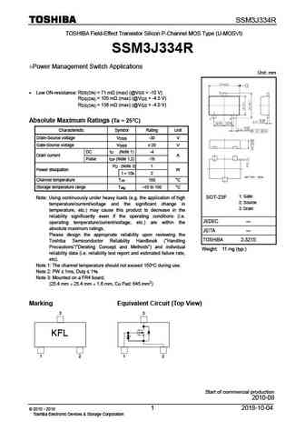
SSM3J334R TOSHIBA Field-Effect Transistor Silicon P-Channel MOS Type (U-MOSVI) SSM3J334R Power Management Switch Applications Unit mm Low ON-resistance R = 71 m (max) (@V = -10 V) DS(ON) GS R = 105 m (max) (@V = -4.5 V) DS(ON) GS R = 136 m (max) (@V = -4.0 V) DS(ON) GS Absolute Maximum Ratings (Ta = 25 C) Characteristic Symbol Rating Unit Drain-Source v
8.12. Size:243K toshiba
ssm3j304t.pdf
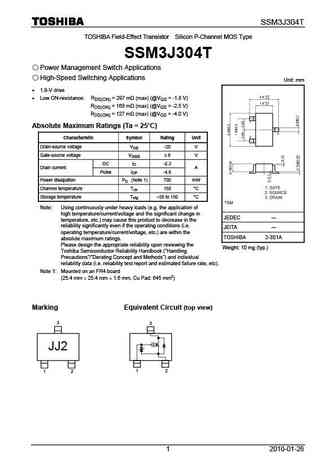
SSM3J304T TOSHIBA Field-Effect Transistor Silicon P-Channel MOS Type SSM3J304T Power Management Switch Applications High-Speed Switching Applications Unit mm 1.8-V drive Low ON-resistance RDS(ON) = 297 m (max) (@VGS = -1.8 V) RDS(ON) = 168 m (max) (@VGS = -2.5 V) RDS(ON) = 127 m (max) (@VGS = -4.0 V) Absolute Maximum Ratings (Ta = 25 C) Character
8.14. Size:230K toshiba
ssm3j331r.pdf
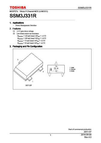
SSM3J331R MOSFETs Silicon P-Channel MOS (U-MOS ) SSM3J331R SSM3J331R SSM3J331R SSM3J331R 1. Applications 1. Applications 1. Applications 1. Applications Power Management Switches 2. Features 2. Features 2. Features 2. Features (1) 1.5-V gate drive voltage. (2) Low drain-source on-resistance RDS(ON) = 150 m (max) (@VGS = -1.5 V) RDS(ON) = 100 m (max) (@VGS = -1.8
8.16. Size:228K toshiba
ssm3j351r.pdf

SSM3J351R MOSFETs Silicon P-Channel MOS (U-MOS ) SSM3J351R SSM3J351R SSM3J351R SSM3J351R 1. Applications 1. Applications 1. Applications 1. Applications Power Management Switches 2. Features 2. Features 2. Features 2. Features (1) 4 V drive (2) Low drain-source on-resistance RDS(ON) = 107 m (typ.) (VGS = -10 V) RDS(ON) = 122 m (typ.) (VGS = -4.5 V) RDS(ON) = 1
8.18. Size:412K toshiba
ssm3j332r.pdf
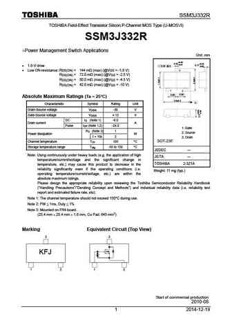
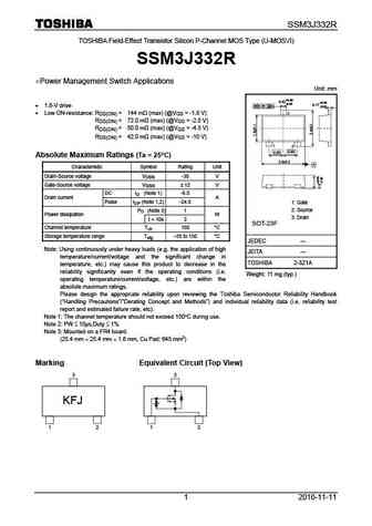
SSM3J332R TOSHIBA Field-Effect Transistor Silicon P-Channel MOS Type (U-MOSVI) SSM3J332R Power Management Switch Applications Unit mm +0.08 0.42 +0.08 -0.05 0.17 1.8-V drive 0.05 M A -0.07 3 Low ON-resistance R = 144 m (max) (@V = -1.8 V) DS(ON) GS R = 72.0 m (max) (@V = -2.5 V) DS(ON) GS R = 50.0 m (max) (@V = -4.5 V) DS(ON) GS R = 42.0 m (m
8.19. Size:211K toshiba
ssm3j317t.pdf
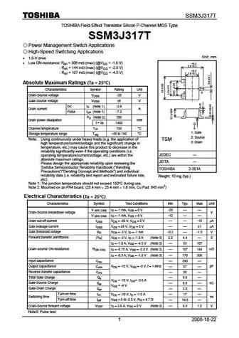
SSM3J317T TOSHIBA Field-Effect Transistor Silicon P-Channel MOS Type SSM3J317T Power Management Switch Applications High-Speed Switching Applications Unit mm 1.8-V drive Low ON-resistance Ron = 306 m (max) (@VGS = -1.8 V) +0.2 2.8-0.3 Ron = 144 m (max) (@VGS = -2.8 V) +0.2 Ron = 107 m (max) (@VGS = -4.5 V) 1.6-0.1 Absolute Maximum Ratings (Ta =
8.20. Size:202K toshiba
ssm3j314t.pdf
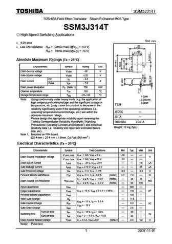
SSM3J314T TOSHIBA Field Effect Transistor Silicon P-Channel MOS Type SSM3J314T High Speed Switching Applications Unit mm 4.0V drive +0.2 Low ON-resistance Ron = 100m (max) (@VGS = -4.0 V) 2.8-0.3 Ron = 54m (max) (@VGS = -10 V) +0.2 1.6-0.1 Absolute Maximum Ratings (Ta = 25 C) Characteristic Symbol Rating Unit Drain-Source voltage VDSS -30
8.21. Size:229K toshiba
ssm3j328r.pdf

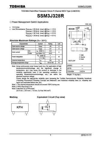
SSM3J328R TOSHIBA Field-Effect Transistor Silicon P-Channel MOS Type (U-MOS ) SSM3J328R Power Management Switch Applications Unit mm +0.08 1.5-V drive 0.42 +0.08 -0.05 0.17 0.05 M A -0.07 Low ON-resistance RDS(ON) = 88.4m (max) (@VGS = -1.5 V) 3 RDS(ON) = 56.0m (max) (@VGS = -1.8 V) RDS(ON) = 39.7m (max) (@VGS = -2.5 V) RDS(ON) = 29.8m (max) (@V
8.22. Size:173K toshiba
ssm3j305t.pdf
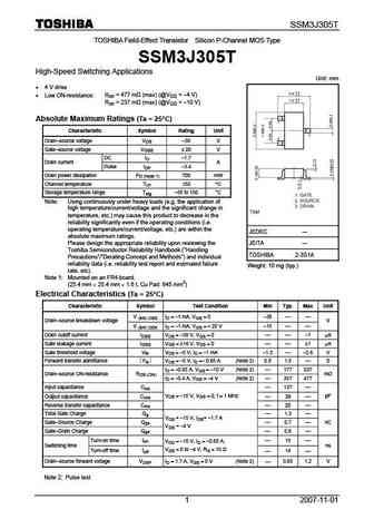
SSM3J305T TOSHIBA Field-Effect Transistor Silicon P-Channel MOS Type SSM3J305T High-Speed Switching Applications Unit mm 4 V drive Low ON-resistance Ron = 477 m (max) (@VGS = -4 V) Ron = 237 m (max) (@VGS = -10 V) Absolute Maximum Ratings (Ta = 25 C) Characteristic Symbol Rating Unit Drain source voltage VDS -30 V Gate source voltage VGSS 20 V DC ID
8.23. Size:207K toshiba
ssm3j321t.pdf
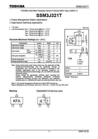
SSM3J321T TOSHIBA Field-Effect Transistor Silicon P-Channel MOS Type (U-MOS V) SSM3J321T Power Management Switch Applications High-Speed Switching Applications 1.5V drive Unit mm Low ON-resistance Ron = 137m (max) (@VGS = -1.5 V) +0.2 Ron = 88m (max) (@VGS = -1.8 V) 2.8-0.3 Ron = 62m (max) (@VGS = -2.5 V) +0.2 1.6-0.1 Ron = 46m (max) (@VGS = -4.5
8.26. Size:345K toshiba
ssm3j35ct.pdf
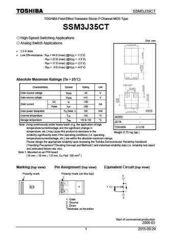
SSM3J35CT TOSHIBA Field-Effect Transistor Silicon P-Channel MOS Type SSM3J35CT High-Speed Switching Applications Unit mm Analog Switch Applications 1.2-V drive Low ON-resistance R = 44 (max) (@V = -1.2 V) on GS R = 22 (max) (@V = -1.5 V) on GS R = 11 (max) (@V = -2.5 V) on GS R = 8 (max) (@V = -4.0 V) on GS Absolute Maximum Ratin
8.28. Size:867K cn vbsemi
ssm3j332r.pdf
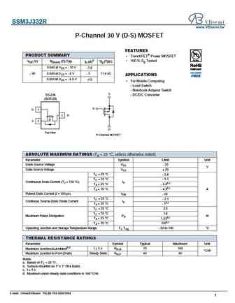
SSM3J332R www.VBsemi.tw P-Channel 30 V (D-S) MOSFET FEATURES PRODUCT SUMMARY TrenchFET Power MOSFET 100 % Rg Tested VDS (V) RDS(on) ( ) Typ. ID (A)a Qg (Typ.) 0.046 at VGS = - 10 V - 5.6 0.049 at VGS = - 6 V - 5 11.4 nC - 30 APPLICATIONS 0.054 at VGS = - 4.5 V -4.5 For Mobile Computing - Load Switch - Notebook Adaptor Switch S TO-236 - DC/DC Converter (SOT-2
8.29. Size:910K cn vbsemi
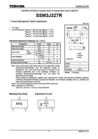
ssm3j327r.pdf
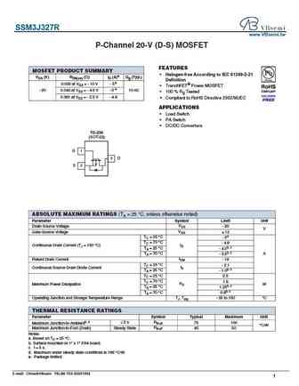
SSM3J327R www.VBsemi.tw P-Channel 20-V (D-S) MOSFET FEATURES MOSFET PRODUCT SUMMARY Halogen-free According to IEC 61249-2-21 VDS (V) RDS(on) ( )ID (A)a Qg (Typ.) Definition 0.035 at VGS = - 10 V - 5e TrenchFET Power MOSFET e - 20 0.043 at VGS = - 4.5 V - 5 10 nC 100 % Rg Tested 0.061 at VGS = - 2.5 V - 4.8 Compliant to RoHS Directive 2002/95/EC APPLICATIO
Otros transistores... SSM3J327F, SSM3J327R, SSM3J328R, SSM3J332R, SSM3J334R, SSM3J35CT, SSM3J35FS, SSM3J35MFV, IRF520, SSM3J36MFV, SSM3J36TU, SSM3J46CTB, SSM3J56MFV, SSM3K01F, SSM3K01T, SSM3K02F, SSM3K02T