SSM3J46CTB MOSFET Equivalente. Reemplazo. Hoja de especificaciones. Principales características
Número de Parte: SSM3J46CTB
Tipo de FET: MOSFET
Polaridad de transistor: P
ESPECIFICACIONES MÁXIMAS
Pdⓘ - Máxima disipación de potencia: 1 W
|Vds|ⓘ - Voltaje máximo drenador-fuente: 20 V
|Vgs|ⓘ - Voltaje máximo fuente-puerta: 8 V
|Id|ⓘ - Corriente continua de drenaje: 2 A
Tjⓘ - Temperatura máxima de unión: 150 °C
CARACTERÍSTICAS ELÉCTRICAS
Cossⓘ - Capacitancia de salida: 44 pF
RDSonⓘ - Resistencia estado encendido drenaje a fuente: 0.103 Ohm
Encapsulados: CST3B
Búsqueda de reemplazo de SSM3J46CTB MOSFET
- Selecciónⓘ de transistores por parámetros
SSM3J46CTB datasheet
ssm3j46ctb.pdf
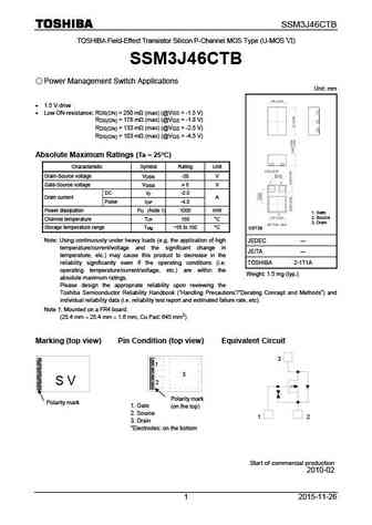
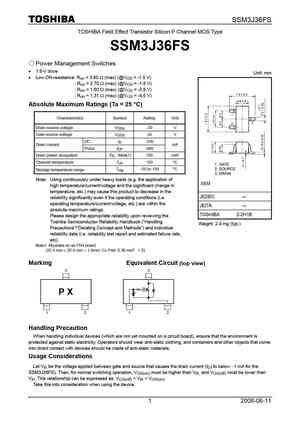
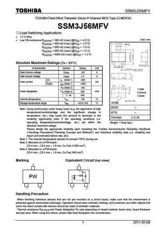
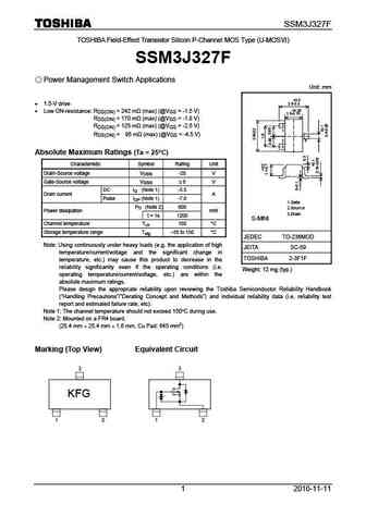
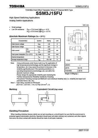
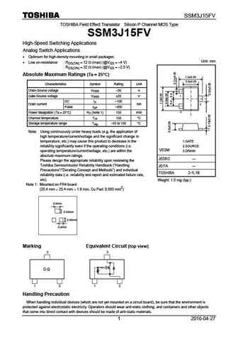
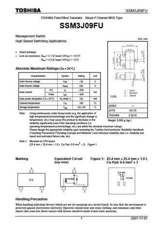
SSM3J46CTB TOSHIBA Field-Effect Transistor Silicon P-Channel MOS Type (U-MOS VI) SSM3J46CTB Power Management Switch Applications Unit mm 1.5 V drive Low ON-resistance R = 250 m (max) (@V = -1.5 V) DS(ON) GS R = 178 m (max) (@V = -1.8 V) DS(ON) GS R = 133 m (max) (@V = -2.5 V) DS(ON) GS R = 103 m (max) (@V = -4.5 V) DS(ON) GS Absolute Maximum Rating
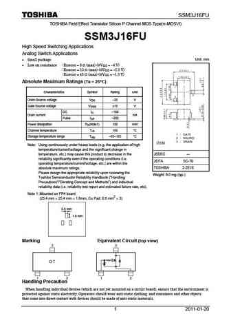
ssm3j16fv.pdf
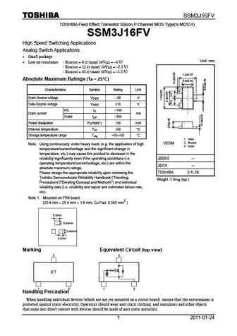
SSM3J16FV TOSHIBA Field Effect Transistor Silicon P Channel MOS Type( -MOSVI) SSM3J16FV High Speed Switching Applications Analog Switch Applications Small package Unit mm Low on-resistance RDS(ON) = 8 (max) (@VGS = -4 V) RDS(ON) = 12 (max) (@VGS = -2.5 V) RDS(ON) = 45 (max) (@VGS = -1.5 V) 1.2 0.05 Absolute Maximum Ratings (Ta = 25 C) 0.8 0.05
ssm3j109tu.pdf
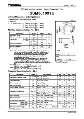
SSM3J109TU TOSHIBA Field-Effect Transistor Silicon P-Channel MOS Type SSM3J109TU Power Management Switch Applications High-Speed Switching Applications Unit mm 1.8 V drive 2.1 0.1 Low ON-resistance Ron = 300 m (max) (@VGS = -1.8 V) 1.7 0.1 Ron = 172 m (max) (@VGS = -2.5 V) Ron = 130 m (max) (@VGS = -4.0 V) 1 Absolute Maximum Ratings (Ta = 25
ssm3j325f.pdf
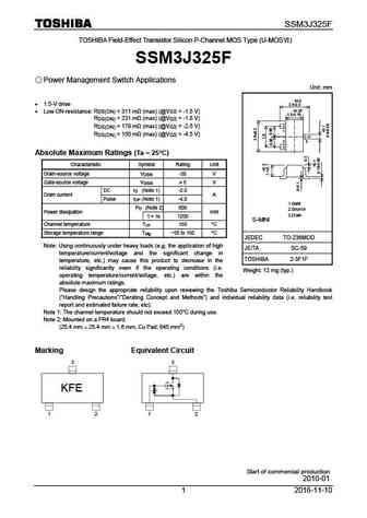
SSM3J325F TOSHIBA Field-Effect Transistor Silicon P-Channel MOS Type (U-MOS ) SSM3J325F Power Management Switch Applications Unit mm +0.5 1.5-V drive 2.5-0.3 +0.25 Low ON-resistance R = 311 m (max) (@V = -1.5 V) DS(ON) GS 1.5-0.15 R = 231 m (max) (@V = -1.8 V) DS(ON) GS R = 179 m (max) (@V = -2.5 V) DS(ON) GS 1 R = 150 m (max) (@V = -4.5 V)
ssm3j356r.pdf
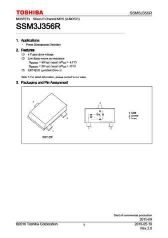
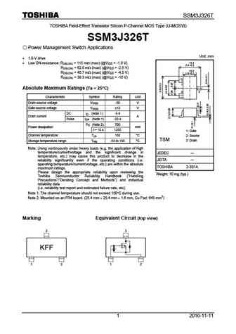
SSM3J356R MOSFETs Silicon P-Channel MOS (U-MOS ) SSM3J356R SSM3J356R SSM3J356R SSM3J356R 1. Applications 1. Applications 1. Applications 1. Applications Power Management Switches 2. Features 2. Features 2. Features 2. Features (1) 4 V gate drive voltage. (2) Low drain-source on-resistance RDS(ON) = 400 m (max) (@VGS = -4.0 V) RDS(ON) = 300 m (max) (@VGS = -10 V)
ssm3j115tu.pdf
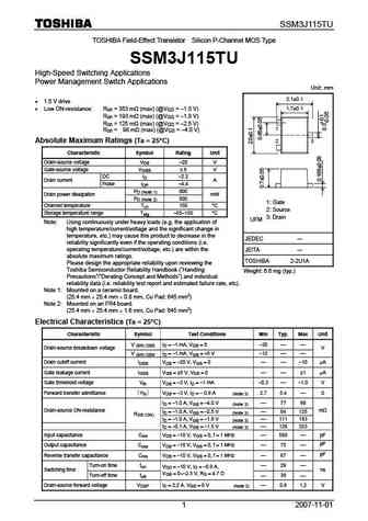
SSM3J115TU TOSHIBA Field-Effect Transistor Silicon P-Channel MOS Type SSM3J115TU High-Speed Switching Applications Power Management Switch Applications Unit mm 2.1 0.1 1.5 V drive 1.7 0.1 Low ON-resistance Ron = 353 m (max) (@VGS = -1.5 V) Ron = 193 m (max) (@VGS = -1.8 V) Ron = 125 m (max) (@VGS = -2.5 V) 1 Ron = 98 m (max) (@VGS = -4.0 V) 3 Ab
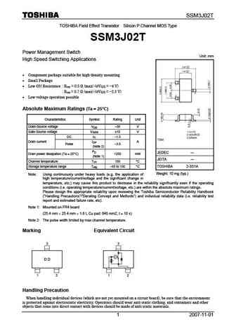
ssm3j01t.pdf
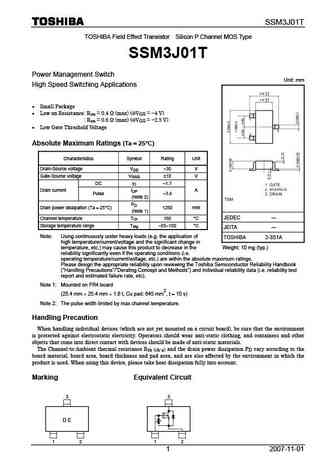
SSM3J01T TOSHIBA Field Effect Transistor Silicon P Channel MOS Type SSM3J01T Power Management Switch Unit mm High Speed Switching Applications Small Package Low on Resistance Ron = 0.4 (max) (@VGS = -4 V) Ron = 0.6 (max) (@VGS = -2.5 V) Low Gate Threshold Voltage Absolute Maximum Ratings (Ta = 25 C) Characteristics Symbol Rating Unit Drain-Source
ssm3j02f.pdf
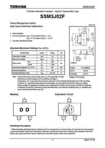
SSM3J02F TOSHIBA Field Effect Transistor Silicon P Channel MOS Type SSM3J02F Power Management Switch Unit mm High Speed Switching Applications Small package Low on resistance Ron = 0.5 (max) (@VGS = -4 V) Ron = 0.7 (max) (@VGS = -2.5 V) Low gate threshold voltage Absolute Maximum Ratings (Ta = 25 C) Characteristics Symbol Rating Unit Drain-source
ssm3j306t.pdf
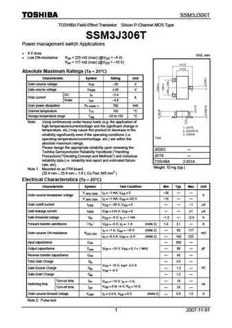
SSM3J306T TOSHIBA Field-Effect Transistor Silicon P-Channel MOS Type SSM3J306T Power management switch Applications 4 V drive Unit mm Low ON-resistance Ron = 225 m (max) (@VGS = -4 V) Ron = 117 m (max) (@VGS = -10 V) Absolute Maximum Ratings (Ta = 25 C) Characteristic Symbol Rating Unit Drain source voltage VDS -30 V Gate source voltage VGSS 20 V DC
ssm3j134tu.pdf
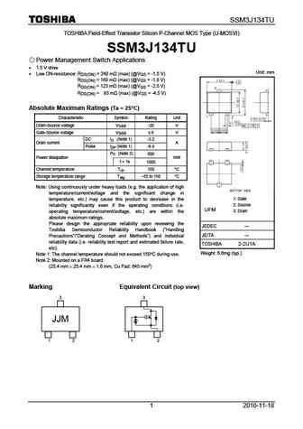
SSM3J134TU TOSHIBA Field-Effect Transistor Silicon P-Channel MOS Type (U-MOS ) SSM3J134TU Power Management Switch Applications 1.5 V drive Unit mm Low ON-resistance RDS(ON) = 240 m (max) (@VGS = -1.5 V) RDS(ON) = 168 m (max) (@VGS = -1.8 V) RDS(ON) = 123 m (max) (@VGS = -2.5 V) RDS(ON) = 93 m (max) (@VGS = -4.5 V) Absolute Maximum Ratings (Ta = 25
ssm3j312t.pdf
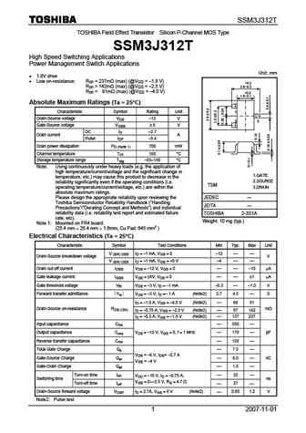
SSM3J312T TOSHIBA Field Effect Transistor Silicon P-Channel MOS Type SSM3J312T High Speed Switching Applications Power Management Switch Applications Unit mm 1.8V drive Low on-resistance Ron = 237m (max) (@VGS = -1.8 V) +0.2 Ron = 142m (max) (@VGS = -2.5 V) 2.8-0.3 Ron = 91m (max) (@VGS = -4.0 V) +0.2 1.6-0.1 Absolute Maximum Ratings (Ta = 25 C) Charac
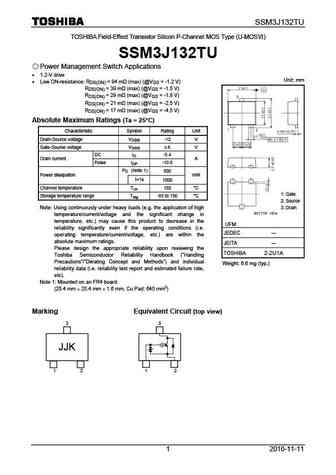
ssm3j132tu.pdf
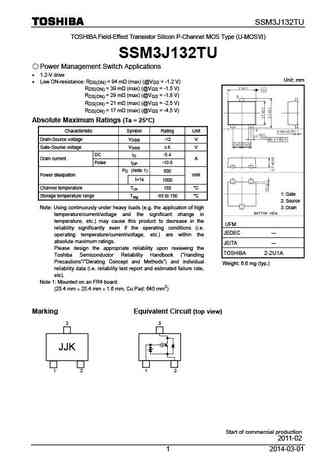
SSM3J132TU TOSHIBA Field-Effect Transistor Silicon P-Channel MOS Type (U-MOS ) SSM3J132TU Power Management Switch Applications 1.2-V drive Unit mm Low ON-resistance RDS(ON) = 94 m (max) (@VGS = -1.2 V) RDS(ON) = 39 m (max) (@VGS = -1.5 V) RDS(ON) = 29 m (max) (@VGS = -1.8 V) RDS(ON) = 21 m (max) (@VGS = -2.5 V) RDS(ON) = 17 m (max) (@VGS = -4.5
ssm3j35mfv.pdf
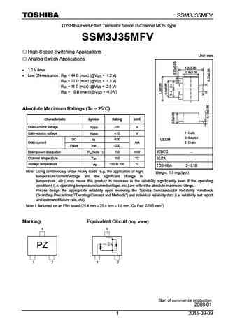
SSM3J35MFV TOSHIBA Field-Effect Transistor Silicon P-Channel MOS Type SSM3J35MFV High-Speed Switching Applications Unit mm Analog Switch Applications 1.2 0.05 1.2 V drive 0.8 0.05 Low ON-resistance R = 44 (max) (@V = -1.2 V) on GS R = 22 (max) (@V = -1.5 V) on GS 1 R = 11 (max) (@V = -2.5 V) on GS R = 8 (max) (@V = -4.0 V) o
ssm3j307t.pdf
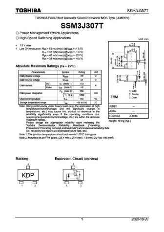
SSM3J307T TOSHIBA Field-Effect Transistor Silicon P-Channel MOS Type (U-MOSV) SSM3J307T Power Management Switch Applications High-Speed Switching Applications Unit mm +0.2 1.5 V drive 2.8-0.3 Low ON-resistance Ron = 83 m (max) (@VGS = -1.5 V) +0.2 1.6-0.1 Ron = 56 m (max) (@VGS = -1.8 V) Ron = 40 m (max) (@VGS = -2.5 V) Ron = 31 m (max) (@VGS = -4.
ssm3j02t.pdf
SSM3J02T TOSHIBA Field Effect Transistor Silicon P Channel MOS Type SSM3J02T Power Management Switch Unit mm High Speed Switching Applications Component package suitable for high-density mounting Small Package Low ON Resistance Ron = 0.5 (max) (@VGS = -4 V) Ron = 0.7 (max) (@VGS = -2.5 V) Low-voltage operation possible Absolute Maximum Ratings
ssm3j338r.pdf
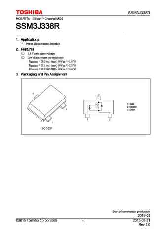
SSM3J338R MOSFETs Silicon P-Channel MOS SSM3J338R SSM3J338R SSM3J338R SSM3J338R 1. Applications 1. Applications 1. Applications 1. Applications Power Management Switches 2. Features 2. Features 2. Features 2. Features (1) 1.8 V gate drive voltage. (2) Low drain-source on-resistance RDS(ON) = 26.3 m (typ.) (@VGS = -1.8 V) RDS(ON) = 20.1 m (typ.) (@VGS = -2.5 V) R
ssm3j334r.pdf
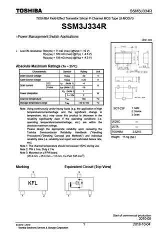
SSM3J334R TOSHIBA Field-Effect Transistor Silicon P-Channel MOS Type (U-MOSVI) SSM3J334R Power Management Switch Applications Unit mm Low ON-resistance R = 71 m (max) (@V = -10 V) DS(ON) GS R = 105 m (max) (@V = -4.5 V) DS(ON) GS R = 136 m (max) (@V = -4.0 V) DS(ON) GS Absolute Maximum Ratings (Ta = 25 C) Characteristic Symbol Rating Unit Drain-Source v
ssm3j36fs.pdf
SSM3J36FS TOSHIBA Field Effect Transistor Silicon P Channel MOS Type SSM3J36FS Power Management Switches 1.5-V drive Unit mm Low ON-resistance Ron = 3.60 (max) (@VGS = -1.5 V) Ron = 2.70 (max) (@VGS = -1.8 V) Ron = 1.60 (max) (@VGS = -2.8 V) Ron = 1.31 (max) (@VGS = -4.5 V) Absolute Maximum Ratings (Ta = 25 C) Characteristics Symbol Rating
ssm3j304t.pdf
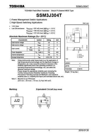
SSM3J304T TOSHIBA Field-Effect Transistor Silicon P-Channel MOS Type SSM3J304T Power Management Switch Applications High-Speed Switching Applications Unit mm 1.8-V drive Low ON-resistance RDS(ON) = 297 m (max) (@VGS = -1.8 V) RDS(ON) = 168 m (max) (@VGS = -2.5 V) RDS(ON) = 127 m (max) (@VGS = -4.0 V) Absolute Maximum Ratings (Ta = 25 C) Character
ssm3j110tu.pdf
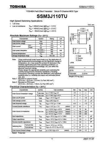
SSM3J110TU TOSHIBA Field Effect Transistor Silicon P-Channel MOS Type SSM3J110TU High Speed Switching Applications 1.8V drive Unit mm Low on-resistance Ron = 240m (max) (@VGS = -1.8 V) Ron = 145m (max) (@VGS = -2.5 V) 2.1 0.1 Ron = 94m (max) (@VGS = -4.0 V) 1.7 0.1 Absolute Maximum Ratings (Ta = 25 C) 1 Characteristic Symbol Rating Unit 3 2 Drain-Sou
ssm3j56mfv.pdf
SSM3J56MFV TOSHIBA Field-Effect Transistor Silicon P-Channel MOS Type (U-MOS ) SSM3J56MFV Load Switching Applications 1.2 V drive Unit mm Low ON-resistance RDS(ON) = 390 m (max) (@VGS = -4.5 V) RDS(ON) = 480 m (max) (@VGS = -2.5 V) RDS(ON) = 660 m (max) (@VGS = -1.8 V) RDS(ON) = 900 m (max) (@VGS = -1.5 V) RDS(ON) = 4000 m (max) (@VGS = -1.2 V)
ssm3j05fu.pdf
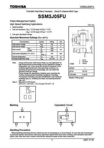
SSM3J05FU TOSHIBA Field Effect Transistor Silicon P Channel MOS Type SSM3J05FU Power Management Switch High Speed Switching Applications Unit mm Small package Low on resistance Ron = 3.3 (max) (@VGS = -4 V) Ron = 4.0 (max) (@VGS = -2.5 V) Low gate threshold voltage Absolute Maximum Ratings (Ta = 25 C) Characteristics Symbol Rating Unit Drain-sour
ssm3j15fs.pdf
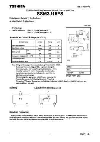
SSM3J15FS TOSHIBA Field Effect Transistor Silicon P Channel MOS Type SSM3J15FS High Speed Switching Applications Analog Switch Applications Unit mm Small package Low ON resistance Ron = 12 (max) (@VGS = -4 V) Ron = 32 (max) (@VGS = -2.5 V) Absolute Maximum Ratings (Ta = 25 C) Characteristics Symbol Rating Unit Drain-Source voltage VDS -30 V Gate-Source v
ssm3j331r.pdf
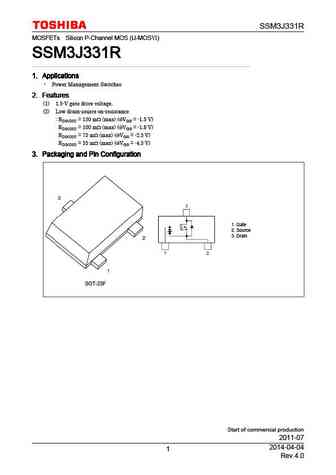
SSM3J331R MOSFETs Silicon P-Channel MOS (U-MOS ) SSM3J331R SSM3J331R SSM3J331R SSM3J331R 1. Applications 1. Applications 1. Applications 1. Applications Power Management Switches 2. Features 2. Features 2. Features 2. Features (1) 1.5-V gate drive voltage. (2) Low drain-source on-resistance RDS(ON) = 150 m (max) (@VGS = -1.5 V) RDS(ON) = 100 m (max) (@VGS = -1.8
ssm3j120tu.pdf
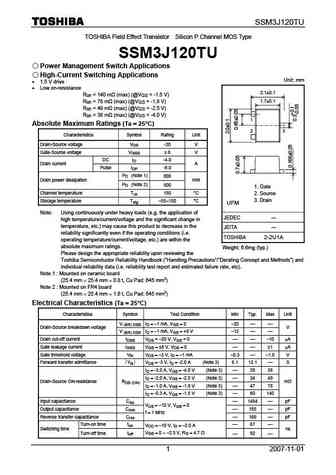
SSM3J120TU TOSHIBA Field Effect Transistor Silicon P Channel MOS Type SSM3J120TU Power Management Switch Applications High-Current Switching Applications Unit mm 1.5 V drive Low on-resistance 2.1 0.1 Ron = 140 m (max) (@VGS = -1.5 V) Ron = 78 m (max) (@VGS = -1.8 V) 1.7 0.1 Ron = 49 m (max) (@VGS = -2.5 V) Ron = 38 m (max) (@VGS = -4.0 V) 1
ssm3j113tu.pdf
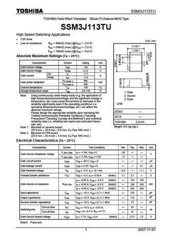
SSM3J113TU TOSHIBA Field Effect Transistor Silicon P-Channel MOS Type SSM3J113TU High Speed Switching Applications 2.0V drive Unit mm Low on-resistance Ron = 449m (max) (@VGS = -2.0 V) 2.1 0.1 Ron = 249m (max) (@VGS = -2.5 V) 1.7 0.1 Ron = 169m (max) (@VGS = -4.0 V) Absolute Maximum Ratings (Ta = 25 C) 1 Characteristic Symbol Rating Unit 3 2 Drain-
ssm3j351r.pdf

SSM3J351R MOSFETs Silicon P-Channel MOS (U-MOS ) SSM3J351R SSM3J351R SSM3J351R SSM3J351R 1. Applications 1. Applications 1. Applications 1. Applications Power Management Switches 2. Features 2. Features 2. Features 2. Features (1) 4 V drive (2) Low drain-source on-resistance RDS(ON) = 107 m (typ.) (VGS = -10 V) RDS(ON) = 122 m (typ.) (VGS = -4.5 V) RDS(ON) = 1
ssm3j130tu.pdf
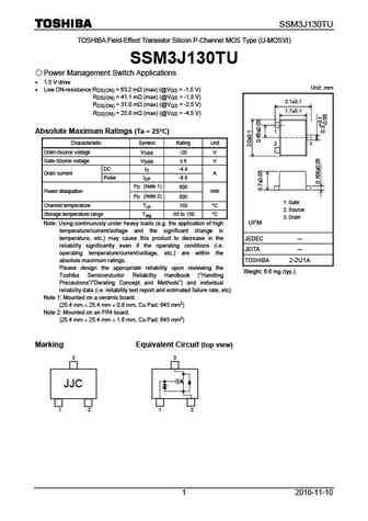
SSM3J130TU TOSHIBA Field-Effect Transistor Silicon P-Channel MOS Type (U-MOS ) SSM3J130TU Power Management Switch Applications 1.5 V drive Unit mm Low ON-resistance RDS(ON) = 63.2 m (max) (@VGS = -1.5 V) RDS(ON) = 41.1 m (max) (@VGS = -1.8 V) 2.1 0.1 RDS(ON) = 31.0 m (max) (@VGS = -2.5 V) 1.7 0.1 RDS(ON) = 25.8 m (max) (@VGS = -4.5 V) 1 Absolu
ssm3j15fu.pdf
SSM3J15FU TOSHIBA Field Effect Transistor Silicon P Channel MOS Type SSM3J15FU High Speed Switching Applications Analog Switch Applications Unit mm Small package Low ON resistance Ron = 12 (max) (@VGS = -4 V) Ron = 32 (max) (@VGS = -2.5 V) Absolute Maximum Ratings (Ta = 25 C) Characteristics Symbol Rating Unit Drain-Source voltage VDS -30 V Gate-Source v
ssm3j118tu.pdf
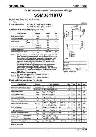
SSM3J118TU TOSHIBA Field-Effect Transistor Silicon P-Channel MOS Type SSM3J118TU High-Speed Switching Applications 4 V drive Unit mm Low ON-resistance Ron = 480 m (max) (@VGS = -4 V) 2.1 0.1 Ron = 240 m (max) (@VGS = -10 V) 1.7 0.1 Absolute Maximum Ratings (Ta = 25 C) Characteristic Symbol Rating Unit 1 Drain source voltage VDS -30 V 3 2 Gate sour
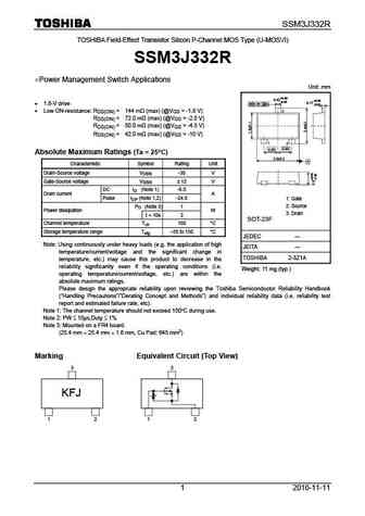
ssm3j332r.pdf
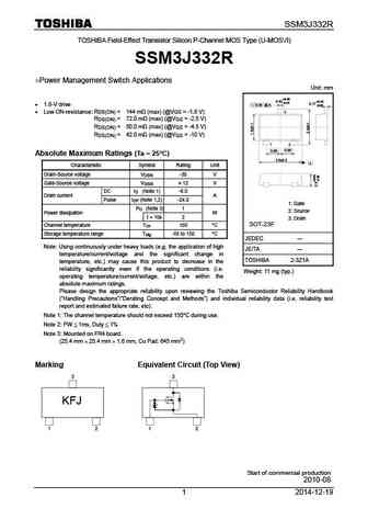
SSM3J332R TOSHIBA Field-Effect Transistor Silicon P-Channel MOS Type (U-MOSVI) SSM3J332R Power Management Switch Applications Unit mm +0.08 0.42 +0.08 -0.05 0.17 1.8-V drive 0.05 M A -0.07 3 Low ON-resistance R = 144 m (max) (@V = -1.8 V) DS(ON) GS R = 72.0 m (max) (@V = -2.5 V) DS(ON) GS R = 50.0 m (max) (@V = -4.5 V) DS(ON) GS R = 42.0 m (m
ssm3j114tu.pdf
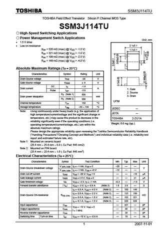
SSM3J114TU TOSHIBA Field Effect Transistor Silicon P Channel MOS Type SSM3J114TU High-Speed Switching Applications Power Management Switch Applications Unit mm 1.5 V drive 2.1 0.1 Low on-resistance Ron = 526 m (max) (@ VGS = -1.5 V) 1.7 0.1 Ron = 321 m (max) (@ VGS = -1.8 V) Ron = 199 m (max) (@ VGS = -2.5 V) 1 Ron = 149 m (max) (@ VGS = -
ssm3j36mfv.pdf
SSM3J36MFV TOSHIBA Field Effect Transistor Silicon P Channel MOS Type SSM3J36MFV Power Management Switches 1.5-V drive Unit mm Low ON-resistance Ron = 3.60 (max) (@VGS = -1.5 V) Ron = 2.70 (max) (@VGS = -1.8 V) 1.2 0.05 Ron = 1.60 (max) (@VGS = -2.8 V) Ron = 1.31 (max) (@VGS = -4.5 V) 0.8 0.05 Absolute Maximum Ratings (Ta = 25 C) 1 Ch
ssm3j129tu.pdf
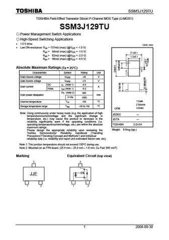
SSM3J129TU TOSHIBA Field-Effect Transistor Silicon P-Channel MOS Type (U-MOSV) SSM3J129TU Power Management Switch Applications High-Speed Switching Applications 1.5 V drive Unit mm Low ON-resistance Ron = 137m (max) (@VGS = -1.5 V) Ron = 88m (max) (@VGS = -1.8 V) 2.1 0.1 Ron = 62m (max) (@VGS = -2.5 V) 1.7 0.1 Ron = 46m (max) (@VGS = -4.5 V) 1
ssm3j317t.pdf
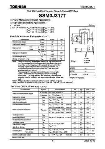
SSM3J317T TOSHIBA Field-Effect Transistor Silicon P-Channel MOS Type SSM3J317T Power Management Switch Applications High-Speed Switching Applications Unit mm 1.8-V drive Low ON-resistance Ron = 306 m (max) (@VGS = -1.8 V) +0.2 2.8-0.3 Ron = 144 m (max) (@VGS = -2.8 V) +0.2 Ron = 107 m (max) (@VGS = -4.5 V) 1.6-0.1 Absolute Maximum Ratings (Ta =
ssm3j14t.pdf
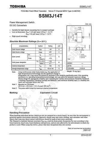
SSM3J14T TOSHIBA Field Effect Transistor Silicon P Channel MOS Type (U-MOSII) SSM3J14T Power Management Switch Unit mm DC-DC Converters Suitable for high-density mounting due to compact package Low on Resistance Ron = 145 m (max) (@VGS = -4.5 V) Ron = 85 m (max) (@VGS = -10 V) High-speed switching Absolute Maximum Ratings (Ta = 25 C) Characteristics
ssm3j133tu.pdf
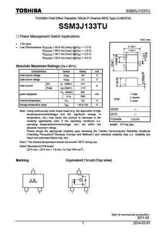
SSM3J133TU TOSHIBA Field Effect Transistor Silicon P-Channel MOS Type (U-MOS ) SSM3J133TU Power Management Switch Applications Unit mm 1.5V drive 2.1 0.1 Low ON-resistance RDS(ON) = 88.4 m (max) (@VGS = -1.5 V) RDS(ON) = 56.0 m (max) (@VGS = -1.8 V) 1.7 0.1 RDS(ON) = 39.7 m (max) (@VGS = -2.5 V) RDS(ON) = 29.8 m (max) (@VGS = -4.5 V) 1 3 2 Absolut
ssm3j314t.pdf
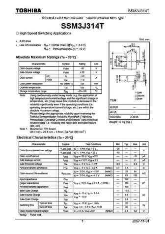
SSM3J314T TOSHIBA Field Effect Transistor Silicon P-Channel MOS Type SSM3J314T High Speed Switching Applications Unit mm 4.0V drive +0.2 Low ON-resistance Ron = 100m (max) (@VGS = -4.0 V) 2.8-0.3 Ron = 54m (max) (@VGS = -10 V) +0.2 1.6-0.1 Absolute Maximum Ratings (Ta = 25 C) Characteristic Symbol Rating Unit Drain-Source voltage VDSS -30
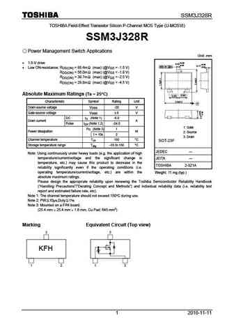
ssm3j328r.pdf

SSM3J328R TOSHIBA Field-Effect Transistor Silicon P-Channel MOS Type (U-MOS ) SSM3J328R Power Management Switch Applications Unit mm +0.08 1.5-V drive 0.42 +0.08 -0.05 0.17 0.05 M A -0.07 Low ON-resistance RDS(ON) = 88.4m (max) (@VGS = -1.5 V) 3 RDS(ON) = 56.0m (max) (@VGS = -1.8 V) RDS(ON) = 39.7m (max) (@VGS = -2.5 V) RDS(ON) = 29.8m (max) (@V
ssm3j305t.pdf
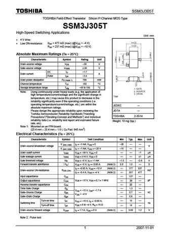
SSM3J305T TOSHIBA Field-Effect Transistor Silicon P-Channel MOS Type SSM3J305T High-Speed Switching Applications Unit mm 4 V drive Low ON-resistance Ron = 477 m (max) (@VGS = -4 V) Ron = 237 m (max) (@VGS = -10 V) Absolute Maximum Ratings (Ta = 25 C) Characteristic Symbol Rating Unit Drain source voltage VDS -30 V Gate source voltage VGSS 20 V DC ID
ssm3j15te.pdf
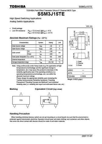
SSM3J15TE TOSHIBA Field Effect Transistor Silicon P Channel MOS Type SSM3J15TE High Speed Switching Applications Analog Switch Applications Unit mm Small package Low ON resistance Ron = 12 (max) (@VGS = -4 V) Ron = 32 (max) (@VGS = -2.5 V) Absolute Maximum Ratings (Ta = 25 C) Characteristics Symbol Rating Unit Drain-Source voltage VDS -30 V Gate-Source v
ssm3j13t.pdf
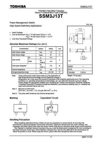
SSM3J13T TOSHIBA Field Effect Transistor Silicon P Channel MOS Type (U-MOSII) SSM3J13T Power Management Switch Unit mm High Speed Switching Applications Small Package Low on Resistance Ron = 70 m (max) (@VGS = -4 V) Ron = 95 m (max) (@VGS = -2.5 V) Low Gate Threshold Voltage Absolute Maximum Ratings (Ta = 25 C) Characteristics Symbol Rating Unit Dr
ssm3j117tu.pdf
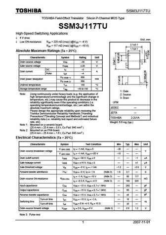
SSM3J117TU TOSHIBA Field-Effect Transistor Silicon P-Channel MOS Type SSM3J117TU High-Speed Switching Applications 4 V drive Unit mm Low ON-resistance Ron = 225 m (max) (@VGS = -4 V) 2.1 0.1 Ron = 117 m (max) (@VGS = -10 V) 1.7 0.1 Absolute Maximum Ratings (Ta = 25 C) Characteristic Symbol Rating Unit 1 Drain source voltage VDS -30 V 3 2 Gate sour
ssm3j01f.pdf
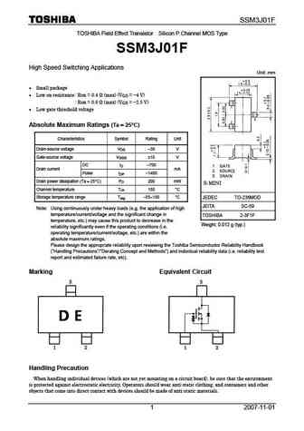
SSM3J01F TOSHIBA Field Effect Transistor Silicon P Channel MOS Type SSM3J01F High Speed Switching Applications Unit mm Small package Low on resistance Ron = 0.4 (max) (VGS = -4 V) Ron = 0.6 (max) (VGS = -2.5 V) Low gate threshold voltage Absolute Maximum Ratings (Ta = 25 C) Characteristics Symbol Rating Unit Drain-source voltage VDS -30 V Gate-so
ssm3j15f.pdf
SSM3J15F TOSHIBA Field Effect Transistor Silicon P Channel MOS Type SSM3J15F High Speed Switching Applications Analog Switch Applications Unit mm Small package +0.5 Low ON resistance Ron = 12 (max) (@VGS = -4 V) 2.5-0.3 +0.25 Ron = 32 (max) (@VGS = -2.5 V) 1.5-0.15 Absolute Maximum Ratings (Ta = 25 C) 1 2 3 Characteristics Symbol Rating Unit Drain-Sou
ssm3j16fu.pdf
SSM3J16FU TOSHIBA Field Effect Transistor Silicon P Channel MOS Type( -MOSVI) SSM3J16FU High Speed Switching Applications Analog Switch Applications Unit mm Small package Low on-resistance RDS(ON) = 8 (max) (@VGS = -4 V) RDS(ON) = 12 (max) (@VGS = -2.5 V) RDS(ON) = 45 (max) (@VGS = -1.5 V) Absolute Maximum Ratings (Ta = 25 C) Characteristics Symbol
ssm3j321t.pdf
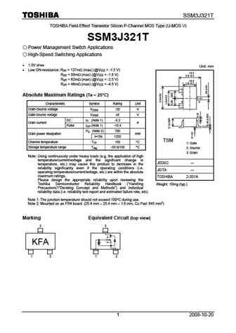
SSM3J321T TOSHIBA Field-Effect Transistor Silicon P-Channel MOS Type (U-MOS V) SSM3J321T Power Management Switch Applications High-Speed Switching Applications 1.5V drive Unit mm Low ON-resistance Ron = 137m (max) (@VGS = -1.5 V) +0.2 Ron = 88m (max) (@VGS = -1.8 V) 2.8-0.3 Ron = 62m (max) (@VGS = -2.5 V) +0.2 1.6-0.1 Ron = 46m (max) (@VGS = -4.5
ssm3j15fv.pdf
SSM3J15FV TOSHIBA Field Effect Transistor Silicon P Channel MOS Type SSM3J15FV High-Speed Switching Applications Analog Switch Applications Optimum for high-density mounting in small packages Unit mm Low on-resistance RDS(ON) = 12 (max) (@VGS = -4 V) RDS(ON) = 32 (max) (@VGS = -2.5 V) Absolute Maximum Ratings (Ta = 25 C) 1.2 0.05 0.8 0.05 Characterist
ssm3j16fs.pdf
SSM3J16FS TOSHIBA Field Effect Transistor Silicon P Channel MOS Type( -MOSVI) SSM3J16FS High Speed Switching Applications Analog Switch Applications Unit mm Small package Low on-resistance RDS(ON) = 8 (max) (@VGS = -4 V) RDS(ON) = 12 (max) (@VGS = -2.5 V) RDS(ON) = 45 (max) (@VGS = -1.5 V) Absolute Maximum Ratings (Ta = 25 C) Characteristics Symbol
ssm3j56act.pdf
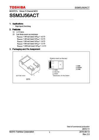
SSM3J56ACT MOSFETs Silicon P-Channel MOS SSM3J56ACT SSM3J56ACT SSM3J56ACT SSM3J56ACT 1. Applications 1. Applications 1. Applications 1. Applications High-Speed Switching 2. Features 2. Features 2. Features 2. Features (1) 1.2 V drive (2) Low drain-source on-resistance RDS(ON) = 390 m (max) (@VGS = -4.5 V) RDS(ON) = 480 m (max) (@VGS = -2.5 V) RDS(ON) = 660 m
ssm3j36tu.pdf
SSM3J36TU TOSHIBA Field Effect Transistor Silicon P Channel MOS Type SSM3J36TU Power Management Switches 1.5-V drive Unit mm Low ON-resistance Ron = 3.60 (max) (@VGS = -1.5 V) Ron = 2.70 (max) (@VGS = -1.8 V) 2.1 0.1 Ron = 1.60 (max) (@VGS = -2.8 V) 1.7 0.1 Ron = 1.31 (max) (@VGS = -4.5 V) Absolute Maximum Ratings (Ta = 25 C) 1 3 2
ssm3j16te.pdf
SSM3J16TE TOSHIBA Field Effect Transistor Silicon P Channel MOS Type SSM3J16TE High Speed Switching Applications Analog Switch Applications Unit mm Small package Low on-resistance Ron = 8 (max) (@VGS = -4 V) Ron = 12 (max) (@VGS = -2.5 V) Ron = 45 (max) (@VGS = -1.5 V) Absolute Maximum Ratings (Ta = 25 C) Characteristics Symbol Rating Unit Drain-So
ssm3j108tu.pdf
SSM3J108TU TOSHIBA Field Effect Transistor Silicon P-Channel MOS Type SSM3J108TU High Speed Switching Applications 1.8V drive Unit mm Low on-resistance Ron = 363m (max) (@VGS = -1.8 V) Ron = 230m (max) (@VGS = -2.5 V) 2.1 0.1 Ron = 158m (max) (@VGS = -4.0 V) 1.7 0.1 Absolute Maximum Ratings (Ta = 25 C) 1 Characteristic Symbol Rating Unit 3 2 Drain-So
ssm3j35ct.pdf
SSM3J35CT TOSHIBA Field-Effect Transistor Silicon P-Channel MOS Type SSM3J35CT High-Speed Switching Applications Unit mm Analog Switch Applications 1.2-V drive Low ON-resistance R = 44 (max) (@V = -1.2 V) on GS R = 22 (max) (@V = -1.5 V) on GS R = 11 (max) (@V = -2.5 V) on GS R = 8 (max) (@V = -4.0 V) on GS Absolute Maximum Ratin
ssm3j15ct.pdf
SSM3J15CT TOSHIBA Field Effect Transistor Silicon P-Channel MOS Type SSM3J15CT High-Speed Switching Applications Analog Switch Applications Unit mm Optimum for high-density mounting in small packages Low ON-resistance Ron = 12 (max) (@VGS = -4 V) 0.6 0.05 Ron = 32 (max) (@VGS = -2.5 V) 0.5 0.03 Absolute Maximum Ratings (Ta = 25 C) Characteristics Sy
ssm3j09fu.pdf
SSM3J09FU TOSHIBA Field Effect Transistor Silicon P Channel MOS Type SSM3J09FU Management Switch Unit mm High Speed Switching Applications Small package Low on resistance Ron = 2.7 (max) (@VGS = -10 V) Ron = 4.2 (max) (@VGS = -4 V) Absolute Maximum Ratings (Ta = 25 C) Characteristics Symbol Rating Unit Drain-Source voltage VDS -30 V Gate-Source voltage
ssm3j112tu.pdf
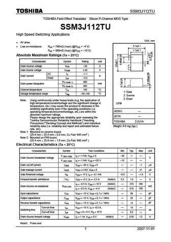
SSM3J112TU TOSHIBA Field Effect Transistor Silicon P-Channel MOS Type SSM3J112TU High Speed Switching Applications Unit mm 4V drive 2.1 0.1 Low on-resistance Ron = 790m (max) (@VGS = -4 V) 1.7 0.1 Ron = 390m (max) (@VGS = -10 V) Absolute Maximum Ratings (Ta = 25 C) 1 Characteristic Symbol Rating Unit 3 2 Drain-Source voltage VDS -30 V Gate-Source volta
ssm3j111tu.pdf
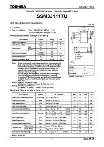
SSM3J111TU TOSHIBA Field Effect Transistor Silicon P-Channel MOS Type SSM3J111TU High Speed Switching Applications Unit mm 2.5V drive 2.1 0.1 Low on-resistance Ron = 480m (max) (@VGS = -4 V) 1.7 0.1 Ron = 680m (max) (@VGS = -2.5 V) Absolute Maximum Ratings (Ta = 25 C) 1 3 2 Characteristic Symbol Rating Unit Drain-Source voltage VDS -20 V Gate-Source vol
ssm3j36fs.pdf
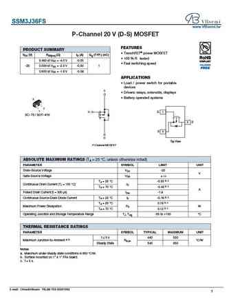
SSM3J36FS www.VBsemi.tw P-Channel 20 V (D-S) MOSFET FEATURES PRODUCT SUMMARY TrenchFET power MOSFET VDS (V) RDS(on) ( )ID (A) Qg (TYP.) (nC) 100 % R tested 0.450 at VGS = -4.5 V -0.55 Fast switching speed -20 0.500 at VGS = -2.5 V -0.50 1 0.600 at VGS = -1.8 V -0.38 APPLICATIONS Load / power switch for portable devices S Drivers relays, solenoids, display
ssm3j332r.pdf
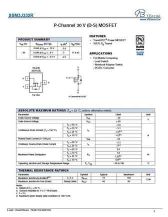
SSM3J332R www.VBsemi.tw P-Channel 30 V (D-S) MOSFET FEATURES PRODUCT SUMMARY TrenchFET Power MOSFET 100 % Rg Tested VDS (V) RDS(on) ( ) Typ. ID (A)a Qg (Typ.) 0.046 at VGS = - 10 V - 5.6 0.049 at VGS = - 6 V - 5 11.4 nC - 30 APPLICATIONS 0.054 at VGS = - 4.5 V -4.5 For Mobile Computing - Load Switch - Notebook Adaptor Switch S TO-236 - DC/DC Converter (SOT-2
ssm3j14t.pdf
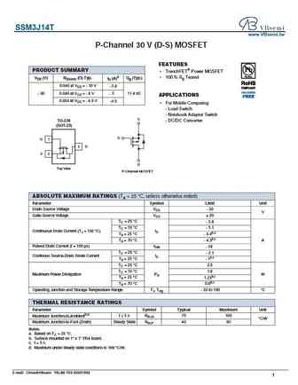
SSM3J14T www.VBsemi.tw P-Channel 30 V (D-S) MOSFET FEATURES PRODUCT SUMMARY TrenchFET Power MOSFET 100 % Rg Tested VDS (V) RDS(on) ( ) Typ. ID (A)a Qg (Typ.) 0.046 at VGS = - 10 V - 5.6 0.049 at VGS = - 6 V - 5 11.4 nC - 30 APPLICATIONS 0.054 at VGS = - 4.5 V -4.5 For Mobile Computing - Load Switch - Notebook Adaptor Switch S TO-236 - DC/DC Converter (SOT-23
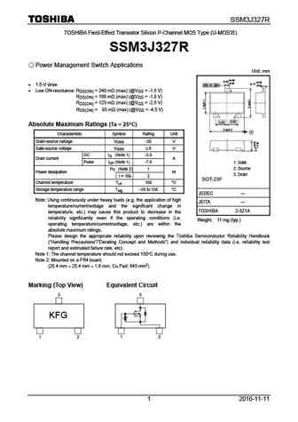
ssm3j327r.pdf
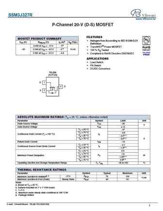
SSM3J327R www.VBsemi.tw P-Channel 20-V (D-S) MOSFET FEATURES MOSFET PRODUCT SUMMARY Halogen-free According to IEC 61249-2-21 VDS (V) RDS(on) ( )ID (A)a Qg (Typ.) Definition 0.035 at VGS = - 10 V - 5e TrenchFET Power MOSFET e - 20 0.043 at VGS = - 4.5 V - 5 10 nC 100 % Rg Tested 0.061 at VGS = - 2.5 V - 4.8 Compliant to RoHS Directive 2002/95/EC APPLICATIO
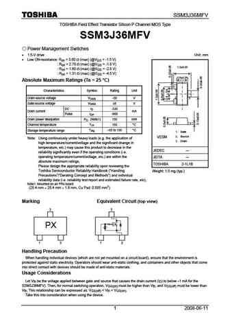
Otros transistores... SSM3J332R, SSM3J334R, SSM3J35CT, SSM3J35FS, SSM3J35MFV, SSM3J36FS, SSM3J36MFV, SSM3J36TU, IRFZ24N, SSM3J56MFV, SSM3K01F, SSM3K01T, SSM3K02F, SSM3K02T, SSM3K05FU, SSM3K09FU, SSM3K101TU
🌐 : EN ES РУ

Liste
Recientemente añadidas las descripciónes de los transistores:
MOSFET: FTF30P35D | FTF25N35DHVT | FTF15N35D | FTE15C35G | FTP02P15G | FTE02P15G | AKF30N5P0SX | AKF30N10S | AKF20P45D | CM4407 | CM3407 | CM3400 | SVF11N65F | SVF11N65T | FKBB3105 | EHBA036R1
Popular searches
mp1620 | kta1381 | bf494 | 2sc1885 | skd502t | 2sb754 | 2sc2362 | 2sd468