TK12A10K3 MOSFET Equivalente. Reemplazo. Hoja de especificaciones. Principales características
Número de Parte: TK12A10K3
Tipo de FET: MOSFET
Polaridad de transistor: N
ESPECIFICACIONES MÁXIMAS
Pdⓘ - Máxima
disipación de potencia: 20 W
|Vds|ⓘ - Voltaje máximo drenador-fuente: 100 V
|Id|ⓘ - Corriente continua
de drenaje: 12 A
CARACTERÍSTICAS ELÉCTRICAS
RDSonⓘ - Resistencia estado encendido drenaje a fuente: 0.08 Ohm
Encapsulados: TO220SIS
Búsqueda de reemplazo de TK12A10K3 MOSFET
- Selecciónⓘ de transistores por parámetros
TK12A10K3 datasheet
9.1. Size:241K toshiba
tk12a60w.pdf 
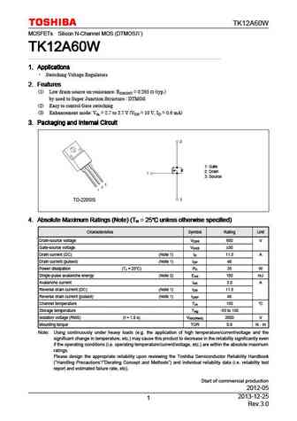
TK12A60W MOSFETs Silicon N-Channel MOS (DTMOS ) TK12A60W TK12A60W TK12A60W TK12A60W 1. Applications 1. Applications 1. Applications 1. Applications Switching Voltage Regulators 2. Features 2. Features 2. Features 2. Features (1) Low drain-source on-resistance RDS(ON) = 0.265 (typ.) by used to Super Junction Structure DTMOS (2) Easy to control Gate switching (3) E
9.2. Size:201K toshiba
tk12a45d.pdf
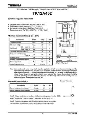
TK12A45D TOSHIBA Field Effect Transistor Silicon N Channel MOS Type ( -MOS ) TK12A45D Switching Regulator Applications Unit mm 2.7 0.2 10 0.3 3.2 0.2 A Low drain-source ON-resistance RDS (ON) = 0.43 (typ.) High forward transfer admittance Yfs = 5.5 S (typ.) Low leakage current IDSS = 10 A (max) (VDS = 450 V) Enhancement-mode
9.3. Size:180K toshiba
tk12a53d.pdf
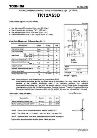
TK12A53D TOSHIBA Field Effect Transistor Silicon N Channel MOS Type ( -MOS ) TK12A53D Switching Regulator Applications Unit mm Low drain-source ON-resistance RDS (ON) = 0.5 (typ.) High forward transfer admittance Yfs = 6.0 S (typ.) Low leakage current IDSS = 10 A (max) (VDS = 525 V) Enhancement mode Vth = 2.0 to 4.0 V (VDS = 10 V, ID = 1 mA)
9.4. Size:238K toshiba
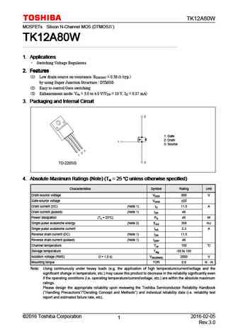
tk12a50w.pdf
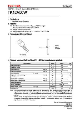
TK12A50W MOSFETs Silicon N-Channel MOS (DTMOS ) TK12A50W TK12A50W TK12A50W TK12A50W 1. Applications 1. Applications 1. Applications 1. Applications Switching Voltage Regulators 2. Features 2. Features 2. Features 2. Features (1) Low drain-source on-resistance RDS(ON) = 0.265 (typ.) by used to Super Junction Structure DTMOS (2) Easy to control Gate switching (3) E
9.5. Size:405K toshiba
tk12a80w.pdf
TK12A80W MOSFETs Silicon N-Channel MOS (DTMOS ) TK12A80W TK12A80W TK12A80W TK12A80W 1. Applications 1. Applications 1. Applications 1. Applications Switching Voltage Regulators 2. Features 2. Features 2. Features 2. Features (1) Low drain-source on-resistance RDS(ON) = 0.38 (typ.) by using Super Junction Structure DTMOS (2) Easy to control Gate switching (3) Enhan
9.6. Size:263K toshiba
tk12a65d.pdf
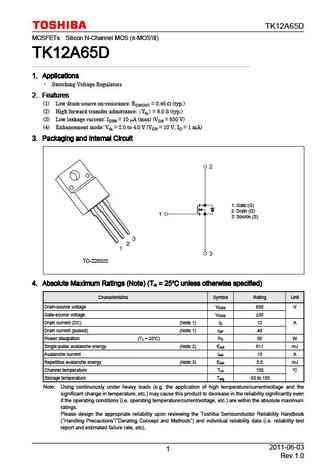
TK12A65D MOSFETs Silicon N-Channel MOS ( -MOS ) TK12A65D TK12A65D TK12A65D TK12A65D 1. Applications 1. Applications 1. Applications 1. Applications Switching Voltage Regulators 2. Features 2. Features 2. Features 2. Features (1) Low drain-source on-resistance RDS(ON) = 0.46 (typ.) (2) High forward transfer admittance Yfs = 6.0 S (typ.) (3) Low leakage current ID
9.7. Size:179K toshiba
tk12a60u.pdf
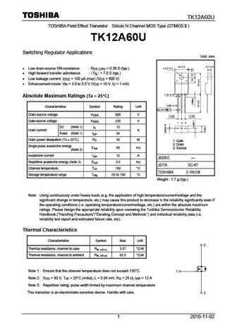
TK12A60U TOSHIBA Field Effect Transistor Silicon N Channel MOS Type (DTMOS ) TK12A60U Switching Regulator Applications Unit mm Low drain-source ON-resistance RDS (ON) = 0.36 (typ.) High forward transfer admittance Yfs = 7.0 S (typ.) Low leakage current IDSS = 100 A (max) (VDS = 600 V) Enhancement-mode Vth = 3.0 to 5.0 V (VDS = 10 V, ID = 1 mA
9.8. Size:185K toshiba
tk12a60d.pdf

TK12A60D TOSHIBA Field Effect Transistor Silicon N Channel MOS Type ( -MOS ) TK12A60D Switching Regulator Applications Unit mm 2.7 0.2 10 0.3 3.2 0.2 A Low drain-source ON resistance RDS (ON) = 0.45 (typ.) High forward transfer admittance Yfs = 7.5 S (typ.) Low leakage current IDSS = 10 A (max) (VDS = 600 V) Enhancement-mod
9.9. Size:276K toshiba
tk12a50d5.pdf
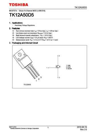
TK12A50D5 MOSFETs Silicon N-Channel MOS ( -MOS ) TK12A50D5 TK12A50D5 TK12A50D5 TK12A50D5 1. Applications 1. Applications 1. Applications 1. Applications Switching Voltage Regulators 2. Features 2. Features 2. Features 2. Features (1) Fast reverse recovery time trrf = 50 ns (typ.), trr = 120 ns (typ.) (2) Low drain-source on-resistance RDS(ON) = 0.5 (typ.) (3) High
9.10. Size:187K toshiba
tk12a55d.pdf
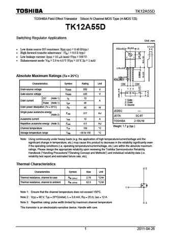
TK12A55D TOSHIBA Field Effect Transistor Silicon N Channel MOS Type ( -MOS VII) TK12A55D Switching Regulator Applications Unit mm 2.7 0.2 10 0.3 3.2 0.2 A Low drain-source ON-resistance RDS (ON) = 0.48 (typ.) High forward transfer admittance Yfs = 6.0 S (typ.) Low leakage current IDSS = 10 A (max) (VDS = 550 V) Enhancement mode Vt
9.11. Size:254K toshiba
tk12a50d.pdf
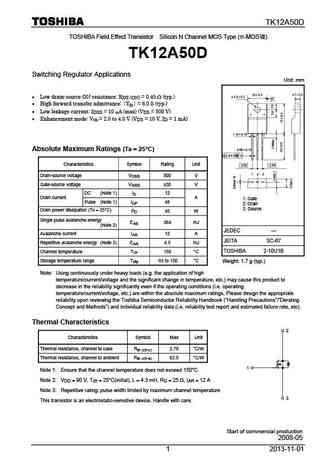
TK12A50D TOSHIBA Field Effect Transistor Silicon N Channel MOS Type ( -MOS ) TK12A50D Switching Regulator Applications Unit mm Low drain-source ON-resistance RDS (ON) = 0.45 (typ.) High forward transfer admittance Yfs = 6.0 S (typ.) Low leakage current IDSS = 10 A (max) (VDS = 500 V) Enhancement mode Vth = 2.0 to 4.0 V (VDS = 10 V, ID = 1 mA) Abs
9.12. Size:253K inchange semiconductor
tk12a60w.pdf
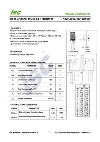
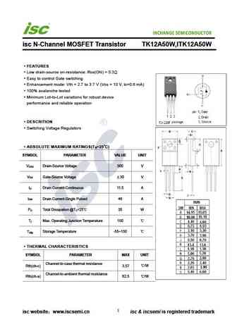
INCHANGE Semiconductor isc N-Channel MOSFET Transistor TK12A60W,ITK12A60W FEATURES Low drain-source on-resistance RDS(ON) = 0.265 (typ.) Easy to control Gate switching Enhancement mode Vth = 2.7 to 3.7 V (VDS = 10 V, ID=0.6 mA) 100% avalanche tested Minimum Lot-to-Lot variations for robust device performance and reliable operation DESCRITION Switching Voltage Regu
9.13. Size:252K inchange semiconductor
tk12a45d.pdf
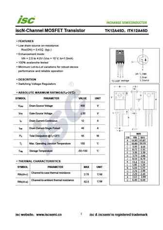
INCHANGE Semiconductor iscN-Channel MOSFET Transistor TK12A45D ITK12A45D FEATURES Low drain-source on-resistance RDS(ON) = 0.43 (typ.) Enhancement mode Vth = 2.0 to 4.0V (VDS = 10 V, ID=1.0mA) 100% avalanche tested Minimum Lot-to-Lot variations for robust device performance and reliable operation DESCRITION Switching Voltage Regulators ABSOLUTE MAXIMUM RATINGS
9.14. Size:252K inchange semiconductor
tk12a53d.pdf
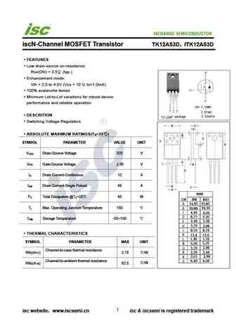
INCHANGE Semiconductor iscN-Channel MOSFET Transistor TK12A53D ITK12A53D FEATURES Low drain-source on-resistance RDS(ON) = 0.5 (typ.) Enhancement mode Vth = 2.0 to 4.0V (VDS = 10 V, ID=1.0mA) 100% avalanche tested Minimum Lot-to-Lot variations for robust device performance and reliable operation DESCRITION Switching Voltage Regulators ABSOLUTE MAXIMUM RATINGS(
9.16. Size:253K inchange semiconductor
tk12a80w.pdf
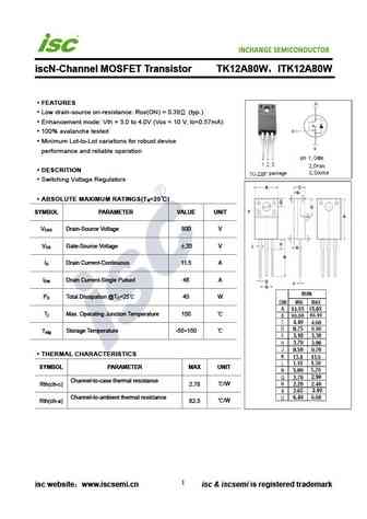
INCHANGE Semiconductor iscN-Channel MOSFET Transistor TK12A80W ITK12A80W FEATURES Low drain-source on-resistance RDS(ON) = 0.38 (typ.) Enhancement mode Vth = 3.0 to 4.0V (VDS = 10 V, ID=0.57mA) 100% avalanche tested Minimum Lot-to-Lot variations for robust device performance and reliable operation DESCRITION Switching Voltage Regulators ABSOLUTE MAXIMUM RATINGS(
9.17. Size:252K inchange semiconductor
tk12a60u.pdf
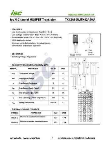
INCHANGE Semiconductor isc N-Channel MOSFET Transistor TK12A60U,ITK12A60U FEATURES Low drain-source on-resistance RDS(ON) = 0.4 Low leakage current IDSS = 100 A (max) (VDS = 600 V) Enhancement mode Vth = 3.0 to 5.0V (VDS = 10 V, ID=1 mA) 100% avalanche tested Minimum Lot-to-Lot variations for robust device performance and reliable operation DESCRITION Switching
9.18. Size:255K inchange semiconductor
tk12a60d.pdf
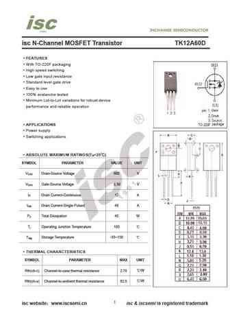
isc N-Channel MOSFET Transistor TK12A60D FEATURES With TO-220F packaging High speed switching Low gate input resistance Standard level gate drive Easy to use 100% avalanche tested Minimum Lot-to-Lot variations for robust device performance and reliable operation APPLICATIONS Power supply Switching applications ABSOLUTE MAXIMUM RATINGS(T =25 ) a SYMBOL PA
9.19. Size:253K inchange semiconductor
tk12a50d5.pdf

INCHANGE Semiconductor iscN-Channel MOSFET Transistor TK12A50D5 ITK12A50D5 FEATURES Low drain-source on-resistance RDS(ON) = 0.5 (typ.) Enhancement mode Vth = 2.5 to 4.5V (VDS = 10 V, ID=1.0mA) 100% avalanche tested Minimum Lot-to-Lot variations for robust device performance and reliable operation DESCRITION Switching Voltage Regulators ABSOLUTE MAXIMUM RATING
Otros transistores... TK10A60D, TK10S04K3L, TK10X40D, TK11A45D, TK11A50D, TK11A55D, TK11A60D, TK11A65D, K2611, TK12A45D, TK12A50D, TK12A53D, TK12A55D, TK12A60D, TK12A60U, TK12A65D, TK12E60U