TK13A45D MOSFET Equivalente. Reemplazo. Hoja de especificaciones. Principales características
Número de Parte: TK13A45D
Tipo de FET: MOSFET
Polaridad de transistor: N
ESPECIFICACIONES MÁXIMAS
Pdⓘ - Máxima
disipación de potencia: 45 W
|Vds|ⓘ - Voltaje máximo drenador-fuente: 450 V
|Vgs|ⓘ - Voltaje máximo fuente-puerta: 30 V
|Id|ⓘ - Corriente continua
de drenaje: 13 A
Tjⓘ - Temperatura máxima de unión: 150 °C
CARACTERÍSTICAS ELÉCTRICAS
trⓘ - Tiempo
de subida: 22 nS
Cossⓘ - Capacitancia de salida: 135 pF
RDSonⓘ - Resistencia estado encendido drenaje a fuente: 0.46 Ohm
Encapsulados: TO220SIS
Búsqueda de reemplazo de TK13A45D MOSFET
- Selecciónⓘ de transistores por parámetros
TK13A45D datasheet
..1. Size:181K toshiba
tk13a45d.pdf 
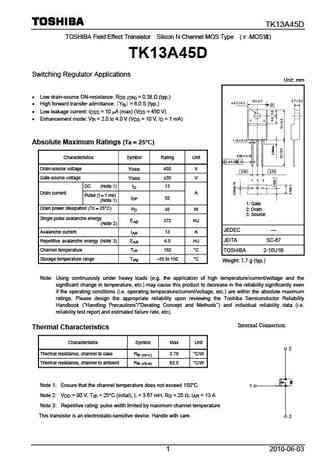
TK13A45D TOSHIBA Field Effect Transistor Silicon N Channel MOS Type ( -MOS ) TK13A45D Switching Regulator Applications Unit mm Low drain-source ON-resistance RDS (ON) = 0.38 (typ.) High forward transfer admittance Yfs = 6.0 S (typ.) Low leakage current IDSS = 10 A (max) (VDS = 450 V) Enhancement mode Vth = 2.0 to 4.0 V (VDS = 10 V, ID = 1 mA)
..2. Size:253K inchange semiconductor
tk13a45d.pdf

INCHANGE Semiconductor iscN-Channel MOSFET Transistor TK13A45D ITK13A45D FEATURES Low drain-source on-resistance RDS(ON) = 0.38 (typ.) Enhancement mode Vth = 2.0 to 4.0V (VDS = 10 V, ID=1.0mA) 100% avalanche tested Minimum Lot-to-Lot variations for robust device performance and reliable operation DESCRITION Switching Voltage Regulators ABSOLUTE MAXIMUM RATINGS
9.1. Size:228K toshiba
tk13a25d.pdf
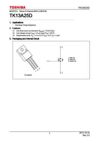
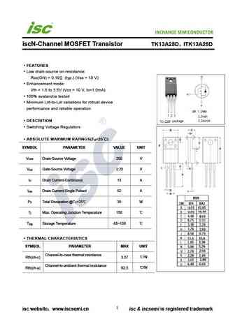
TK13A25D MOSFETs Silicon N-Channel MOS ( -MOS ) TK13A25D TK13A25D TK13A25D TK13A25D 1. Applications 1. Applications 1. Applications 1. Applications Switching Voltage Regulators 2. Features 2. Features 2. Features 2. Features (1) Low drain-source on-resistance RDS(ON) = 0.19 (typ.) (2) Low leakage current IDSS = 10 A (max) (VDS = 250 V) (3) Enhancement mode Vth =
9.2. Size:184K toshiba
tk13a50d.pdf
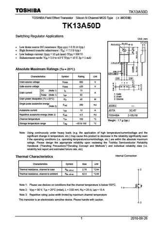
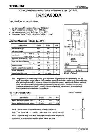
TK13A50D TOSHIBA Field Effect Transistor Silicon N Channel MOS Type ( -MOS ) TK13A50D Switching Regulator Applications Unit mm 2.7 0.2 10 0.3 3.2 0.2 A Low drain-source ON resistance RDS (ON) = 0.31 (typ.) High forward transfer admittance Yfs = 7.5 S (typ.) Low leakage current IDSS = 10 A (max) (VDS = 500 V) Enhancement-mode
9.3. Size:191K toshiba
tk13a60d.pdf
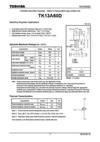
TK13A60D TOSHIBA Field Effect Transistor Silicon N Channel MOS Type ( -MOS VII) TK13A60D Switching Regulator Applications Unit mm Low drain-source ON-resistance RDS (ON) = 0.33 (typ.) High forward transfer admittance Yfs = 6.5 S (typ.) Low leakage current IDSS = 10 A (max) (VDS = 600 V) Enhancement mode Vth = 2.0 to 4.0 V (VDS = 10 V, ID = 1 mA) Ab
9.4. Size:226K toshiba
tk13a65d.pdf
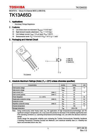
TK13A65D MOSFETs Silicon N-Channel MOS ( -MOS ) TK13A65D TK13A65D TK13A65D TK13A65D 1. Applications 1. Applications 1. Applications 1. Applications Switching Voltage Regulators 2. Features 2. Features 2. Features 2. Features (1) Low drain-source on-resistance RDS(ON) = 0.4 (typ.) (2) High forward transfer admittance Yfs = 7.5 S (typ.) (3) Low leakage current IDS
9.5. Size:191K toshiba
tk13a55da.pdf

TK13A55DA TOSHIBA Field Effect Transistor Silicon N Channel MOS Type ( -MOS ) TK13A55DA Switching Regulator Applications Unit mm 2.7 0.2 10 0.3 3.2 0.2 A Low drain-source ON-resistance RDS (ON) = 0.32 (typ.) High forward transfer admittance Yfs = 6.0 S (typ.) Low leakage current IDSS = 10 A (max) (VDS = 550 V) Enhancement mode Vt
9.6. Size:177K toshiba
tk13a50da.pdf
TK13A50DA TOSHIBA Field Effect Transistor Silicon N Channel MOS Type ( -MOS ) TK13A50DA Switching Regulator Applications Unit mm Low drain-source ON-resistance RDS (ON) = 0.39 (typ.) High forward transfer admittance Yfs = 6.0 S (typ.) Low leakage current IDSS = 10 A (max) (VDS = 500 V) Enhancement mode Vth = 2.0 to 4.0 V (VDS = 10 V, ID = 1 mA
9.7. Size:213K toshiba
tk13a65u.pdf
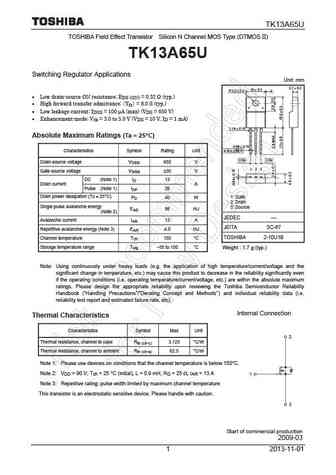
TK13A65U TOSHIBA Field Effect Transistor Silicon N Channel MOS Type (DTMOS II) TK13A65U Switching Regulator Applications Unit mm 2.7 0.2 10 0.3 3.2 0.2 A Low drain-source ON resistance RDS (ON) = 0.32 (typ.) High forward transfer admittance Yfs = 8.0 S (typ.) Low leakage current IDSS = 100 A (max) (VDS = 650 V) Enhancement-mod
9.8. Size:252K inchange semiconductor
tk13a25d.pdf
INCHANGE Semiconductor iscN-Channel MOSFET Transistor TK13A25D ITK13A25D FEATURES Low drain-source on-resistance RDS(ON) = 0.19 (typ.) (VGS = 10 V) Enhancement mode Vth = 1.5 to 3.5V (VDS = 10 V, ID=1.0mA) 100% avalanche tested Minimum Lot-to-Lot variations for robust device performance and reliable operation DESCRITION Switching Voltage Regulators ABSOLUTE MA
9.9. Size:252K inchange semiconductor
tk13a60d.pdf
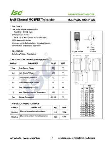
INCHANGE Semiconductor iscN-Channel MOSFET Transistor TK13A60D ITK13A60D FEATURES Low drain-source on-resistance RDS(ON) = 0.33 (typ.) Enhancement mode Vth = 2.0 to 4.0V (VDS = 10 V, ID=1.0mA) 100% avalanche tested Minimum Lot-to-Lot variations for robust device performance and reliable operation DESCRITION Switching Voltage Regulators ABSOLUTE MAXIMUM RATINGS
9.10. Size:255K inchange semiconductor
tk13a60w.pdf
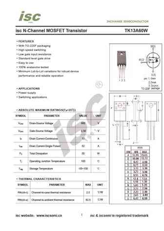
isc N-Channel MOSFET Transistor TK13A60W FEATURES With TO-220F packaging High speed switching Low gate input resistance Standard level gate drive Easy to use 100% avalanche tested Minimum Lot-to-Lot variations for robust device performance and reliable operation APPLICATIONS Power supply Switching applications ABSOLUTE MAXIMUM RATINGS(T =25 ) a SYMBOL PA
9.11. Size:257K inchange semiconductor
tk13a65d.pdf
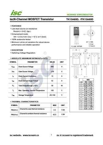
INCHANGE Semiconductor iscN-Channel MOSFET Transistor TK13A65D ITK13A65D FEATURES Low drain-source on-resistance RDS(on) = 0.4 (typ.) Enhancement mode Vth = 2.0 to 4.0V (VDS = 10 V, ID=1.0mA) 100% avalanche tested Minimum Lot-to-Lot variations for robust device performance and reliable operation DESCRITION Switching Voltage Regulators ABSOLUTE MAXIMUM RATINGS(
9.12. Size:253K inchange semiconductor
tk13a50da.pdf
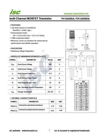
INCHANGE Semiconductor iscN-Channel MOSFET Transistor TK13A50DA ITK13A50DA FEATURES Low drain-source on-resistance RDS(ON) = 0.39 (typ.) Enhancement mode Vth = 2.0 to 4.0V (VDS = 10 V, ID=1.0mA) 100% avalanche tested Minimum Lot-to-Lot variations for robust device performance and reliable operation DESCRITION Switching Voltage Regulators ABSOLUTE MAXIMUM RAT
9.13. Size:253K inchange semiconductor
tk13a65u.pdf
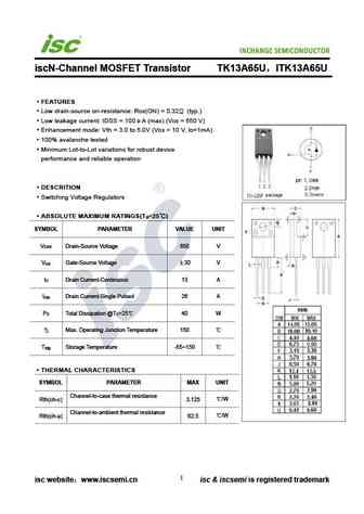
INCHANGE Semiconductor iscN-Channel MOSFET Transistor TK13A65U ITK13A65U FEATURES Low drain-source on-resistance RDS(ON) = 0.32 (typ.) Low leakage current IDSS = 100 A (max) (VDS = 650 V) Enhancement mode Vth = 3.0 to 5.0V (VDS = 10 V, ID=1mA) 100% avalanche tested Minimum Lot-to-Lot variations for robust device performance and reliable operation DESCRITION Sw
Otros transistores... TK12A65D, TK12E60U, TK12J55D, TK12J60U, TK12X53D, TK12X60U, TK130F06K3, TK13A25D, IRF540N, TK13A50DA, TK13A50D, TK13A55DA, TK13A60D, TK13A65D, TK13A65U, TK13E25D, TK13J65U
