2SK3625 Datasheet. Equivalente. Reemplazo. Hoja de especificaciones. Principales características
Número de Parte: 2SK3625 📄📄
Tipo de FET: MOSFET
Polaridad de transistor: N
ESPECIFICACIONES MÁXIMAS
Pdⓘ - Máxima disipación de potencia: 100 W
|Vds|ⓘ - Voltaje máximo drenador-fuente: 200 V
|Vgs|ⓘ - Voltaje máximo fuente-puerta: 30 V
|Id|ⓘ - Corriente continua de drenaje: 25 A
Tjⓘ - Temperatura máxima de unión: 150 °C
CARACTERÍSTICAS ELÉCTRICAS
trⓘ - Tiempo de subida: 20 nS
Cossⓘ - Capacitancia de salida: 1060 pF
RDSonⓘ - Resistencia estado encendido drenaje a fuente: 0.082 Ohm
Encapsulados: TO220FL
📄📄 Copiar
Búsqueda de reemplazo de 2SK3625 MOSFET
- Selecciónⓘ de transistores por parámetros
2SK3625 datasheet
2sk3625.pdf
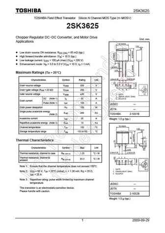
2SK3625 TOSHIBA Field Effect Transistor Silicon N Channel MOS Type ( -MOSV) 2SK3625 Chopper Regulator DC-DC Converter, and Motor Drive Unit mm Applications Low drain-source ON resistance RDS (ON) = 65 m (typ.) High forward transfer admittance Yfs = 10 S (typ.) Low leakage current IDSS = 100 A (max) (VDS = 200 V) Enhancement mode Vth = 3.0 to 5.0 V (VDS = 1
2sk362.pdf
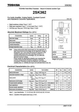
2SK362 TOSHIBA Field Effect Transistor Silicon N Channel Junction Type 2SK362 For Audio Amplifier, Analog Switch, Constant Current Unit mm and Impedance Converter Applications High breakdown voltage VGDS = -50 V High input impedance IGSS = -1.0 nA (max) (VGS = -30 V) Low RDS (ON) RDS (ON) = 80 (typ.) (IDSS = 5 mA) Absolute Maximum Ratings (Ta = 25 C) Cha
2sk3628.pdf
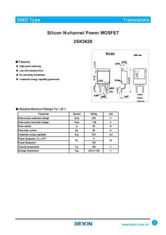
SMD Type IC SMD Type Transistors Silicon N-channel Power MOSFET 2SK3628 TO-263 Unit mm +0.2 Features 4.57-0.2 1.27+0.1 -0.1 High-speed switching Low ON resistance Ron No secondary breakdown Avalanche energy capability guaranteed 0.1max 1.27+0.1 -0.1 +0.1 0.81-0.1 2.54 1Gate 2.54+0.2 +0.2 -0.2 +0.1 5.08-0.1 0.4-0.2 2Drain 3 Source Absolute Maximum Ratings Ta = 25 Para
2sk3670.pdf
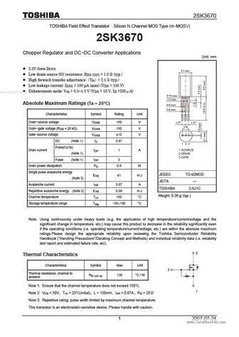
2SK3670 TOSHIBA Field Effect Transistor Silicon N Channel MOS Type ( -MOSV) 2SK3670 Chopper Regulator and DC-DC Converter Applications Unit mm 2.5V-Gate Drive Low drain-source ON resistance RDS (ON) = 1.0 (typ.) High forward transfer admittance Yfs = 2.1 S (typ.) Low leakage current IDSS = 100 A (max) (VDS = 150 V) Enhancement mode Vth = 0.5 1.3 V (VDS
2sk3617.pdf

Ordering number ENN8112 2SK3617 N-Channel Silicon MOSFET 2SK3617 General-Purpose Switching Device Applications Features Low ON-resistance. Ultrahigh-speed switching. 4V drive. Specifications Absolute Maximum Ratings at Ta=25 C Parameter Symbol Conditions Ratings Unit Drain-to-Source Voltage VDSS 100 V Gate-to-Source Voltage VGSS 20 V Drain Current (DC) ID 6 A Drai
2sk3618.pdf
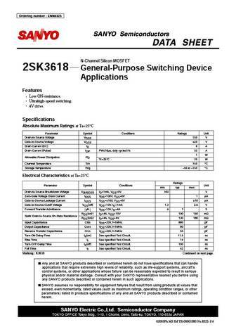
Ordering number ENN8325 2SK3618 N-Channel Silicon MOSFET General-Purpose Switching Device 2SK3618 Applications Features Low ON-resistance. Ultrahigh-speed switching. 4V drive. Specifications Absolute Maximum Ratings at Ta=25 C Parameter Symbol Conditions Ratings Unit Drain-to-Source Voltage VDSS 100 V Gate-to-Source Voltage VGSS 20 V Drain Current (DC) ID 8 A Dra
2sk366.pdf
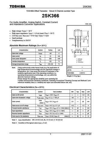
2SK366 TOSHIBA Effect Transistor Silicon N Channel Junction Type 2SK366 For Audio Amplifier, Analog-Switch, Constant Current Unit mm and Impedance Converter Applications High voltage VGDS = -40 V High input impedance IGSS = -1.0 nA (max) (VGS = -30 V) Low RDS (ON) RDS (ON) = 50 (typ.) (IDSS = 5 mA) Small package Complementary to 2SJ107 Absolute
2sk3662.pdf
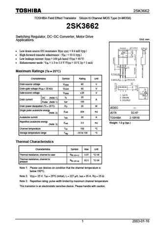
2SK3662 TOSHIBA Field Effect Transistor Silicon N Channel MOS Type ( -MOSII) 2SK3662 Switching Regulator, DC-DC Converter, Motor Drive Unit mm Applications Low drain-source ON resistance RDS (ON) = 9.4 m (typ.) High forward transfer admittance Y = 55 S (typ.) fs Low leakage current I = 100 A (max) (V = 60 V) DSS DS Enhancement-mode Vth = 1.3 to
2sk3669.pdf
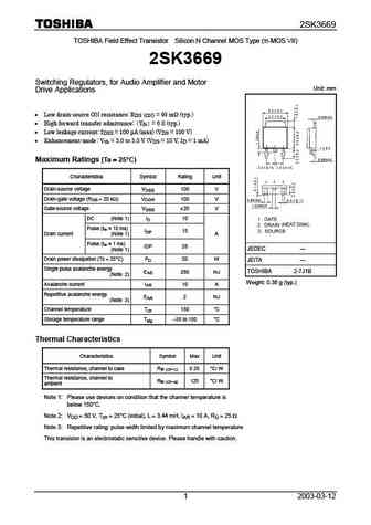
2SK3669 TOSHIBA Field Effect Transistor Silicon N Channel MOS Type ( -MOS VII) 2SK3669 Switching Regulators, for Audio Amplifier and Motor Unit mm Drive Applications Low drain-source ON resistance RDS (ON) = 95 m (typ.) High forward transfer admittance Y = 6 S (typ.) fs Low leakage current I = 100 A (max) (V = 100 V) DSS DS Enhancement-mode Vth
2sk3667.pdf
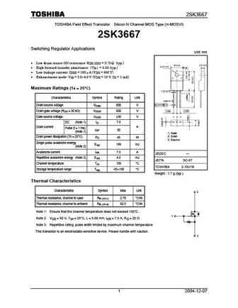
2SK3667 TOSHIBA Field Effect Transistor Silicon N Channel MOS Type ( -MOSVI) 2SK3667 Switching Regulator Applications Unit mm Low drain-source ON resistance RDS (ON) = 0.75 (typ.) High forward transfer admittance Yfs = 5.5S (typ.) Low leakage current IDSS = 100 A (VDS = 600 V) Enhancement mode Vth = 2.0 4.0 V (VDS = 10 V, ID = 1 mA) Maximum Ratings (
2sk3658.pdf
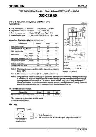
2SK3658 2 TOSHIBA Field Effect Transistor Silicon N Channel MOS Type (L - -MOSV) 2SK3658 DC-DC Converter, Relay Drive and Motor Drive Unit mm Applications Low drain-source ON resistance RDS (ON) = 0.23 (typ.) High forward transfer admittance Yfs = 2.0 S (typ.) Low leakage current IDSS = 100 A (max) (VDS = 60 V) Enhancement-mode Vth = 0.8 to 2.0 V (VD
2sk369.pdf
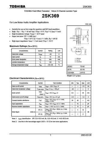
2SK369 TOSHIBA Field Effect Transistor Silicon N Channel Junction Type 2SK369 For Low Noise Audio Amplifier Applications Unit mm Suitable for use as first stage for equalizer and MC head amplifiers. High Y Y = 40 mS (typ.) (V = 10 V, V = 0, I = 5 mA) fs fs DS GS DSS High breakdown voltage V = -40 V (min) GDS Super low noise NF = 1.0dB (typ.) (V = 10
2sk363.pdf
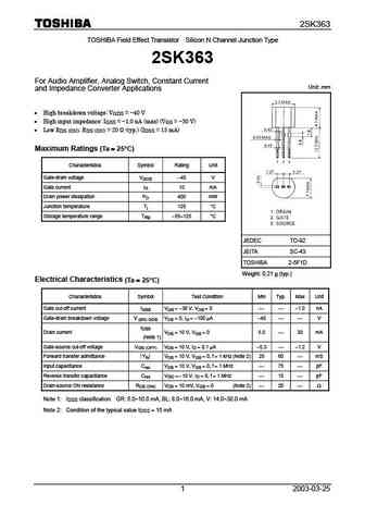
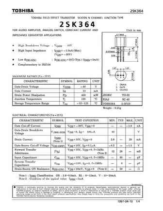
2SK363 TOSHIBA Field Effect Transistor Silicon N Channel Junction Type 2SK363 For Audio Amplifier, Analog Switch, Constant Current Unit mm and Impedance Converter Applications High breakdown voltage VGDS = -40 V High input impedance I = -1.0 nA (max) (V = -30 V) GSS GS Low R R = 20 (typ.) (I = 15 mA) DS (ON) DS (ON) DSS Maximum Ratings (Ta = = 25 C)
2sk365.pdf

2SK365 TOSHIBA Field Effect Transistor Silicon N Channel Junction Type 2SK365 For Audio Amplifier, Analog-Switch, Constant Current Unit mm and Impedance Converter Applications High breakdown voltage VGDS = -50 V High input impedance IGSS = -1.0 nA (max) (VGS = -30 V) Low RDS (ON) RDS (ON) = 80 (typ.) (IDSS = 5 mA) Small package Absolute Maximum Rating
2sk3633.pdf
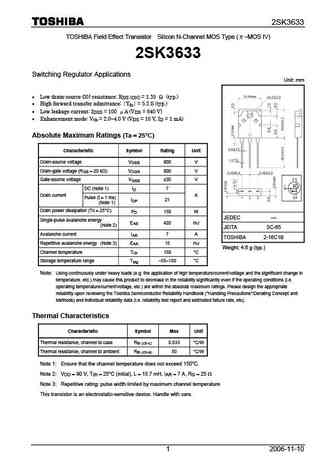
2SK3633 TOSHIBA Field Effect Transistor Silicon N-Channel MOS Type ( -MOS IV) 2SK3633 Switching Regulator Applications Unit mm Low drain-source ON-resistance RDS (ON) = 1.35 (typ.) High forward transfer admittance Yfs = 5.2 S (typ.) Low leakage current IDSS = 100 A (VDS = 640 V) Enhancement mode Vth = 2.0 4.0 V (VDS = 10 V, ID = 1 mA) Absolute Maxi
2sk3656.pdf
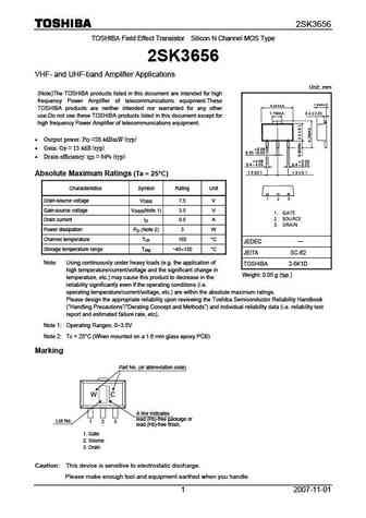
2SK3656 TOSHIBA Field Effect Transistor Silicon N Channel MOS Type 2SK3656 VHF- and UHF-band Amplifier Applications Unit mm (Note)The TOSHIBA products listed in this document are intended for high frequency Power Amplifier of telecommunications equipment.These TOSHIBA products are neither intended nor warranted for any other use.Do not use these TOSHIBA products listed in this
2sk368.pdf
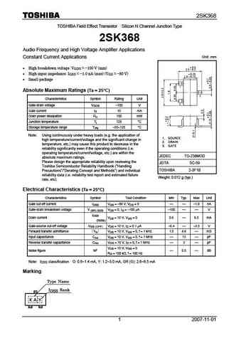
2SK368 TOSHIBA Field Effect Transistor Silicon N Channel Junction Type 2SK368 Audio Frequency and High Voltage Amplifier Applications Unit mm Constant Current Applications High breakdown voltage VGDS = -100 V (min) High input impedance IGSS = -1.0 nA (max) (VGS = -80 V) Small package Absolute Maximum Ratings (Ta = 25 C) Characteristics Symbol Rating Unit Gat
2sk3614.pdf
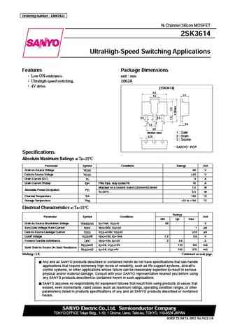
Ordering number ENN7422 2SK3614 N-Channel Silicon MOSFET 2SK3614 UltraHigh-Speed Switching Applications Features Package Dimensions Low ON-resistance. unit mm Ultrahigh-speed switching. 2062A 4V drive. [2SK3614] 4.5 1.5 1.6 0.4 0.5 3 2 1 0.4 1.5 3.0 1 Gate (Bottom view) 2 Drain 0.75 3 Source SANYO PCP Specifications Absolute Maximum Ratings at Ta
2sk3615.pdf
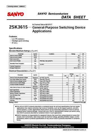
Ordering number ENN8332 2SK3615 N-Channel Silicon MOSFET General-Purpose Switching Device 2SK3615 Applications Features Low ON-resistance. Ultrahigh-speed switching. 4V drive. Specifications Absolute Maximum Ratings at Ta=25 C Parameter Symbol Conditions Ratings Unit Drain-to-Source Voltage VDSS 60 V Gate-to-Source Voltage VGSS 20 V Drain Current (DC) ID 12 A Dra
2sk3666-2-tb-e.pdf
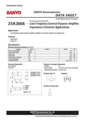
2SK3666 Ordering number EN8158B SANYO Semiconductors DATA SHEET N-Channel Junctin Silicon FET Low-Frequency General-Purpose Amplifier, 2SK3666 Impedance Converter Applications Applications Low-frequency general-purpose amplifier, impedance conversion, infrared sensor applications Features Small IGSS Small Ciss Specifications at Ta=25 C Absolute Maximum Ratings Pa
2sk3659.pdf
To our customers, Old Company Name in Catalogs and Other Documents On April 1st, 2010, NEC Electronics Corporation merged with Renesas Technology Corporation, and Renesas Electronics Corporation took over all the business of both companies. Therefore, although the old company name remains in this document, it is a valid Renesas Electronics document. We appreciate your understanding.
2sk360.pdf
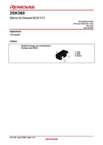
2SK360 Silicon N-Channel MOS FET REJ03G0811-0200 (Previous ADE-208-1170) Rev.2.00 Aug.10.2005 Application VHF amplifier Outline RENESAS Package code PLSP0003ZB-A (Package name MPAK) 1. Gate 3 2. Drain 3. Source 1 2 Rev.2.00, Aug 10.2005, page 1 of 5 2SK360 Absolute Maximum Ratings (Ta = 25 C) Item Symbol Ratings Unit Drain to source voltage VDSX*1 20 V G
2sk3634-z.pdf

To our customers, Old Company Name in Catalogs and Other Documents On April 1st, 2010, NEC Electronics Corporation merged with Renesas Technology Corporation, and Renesas Electronics Corporation took over all the business of both companies. Therefore, although the old company name remains in this document, it is a valid Renesas Electronics document. We appreciate your understanding.
2sk3635-z.pdf

To our customers, Old Company Name in Catalogs and Other Documents On April 1st, 2010, NEC Electronics Corporation merged with Renesas Technology Corporation, and Renesas Electronics Corporation took over all the business of both companies. Therefore, although the old company name remains in this document, it is a valid Renesas Electronics document. We appreciate your understanding.
2sk3653.pdf
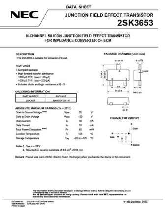
DATA SHEET JUNCTION FIELD EFFECT TRANSISTOR 2SK3653 N-CHANNEL SILICON JUNCTION FIELD EFFECT TRANSISTOR FOR IMPEDANCE CONVERTER OF ECM PACKAGE DRAWING (Unit mm) DESCRIPTION The 2SK3653 is suitable for converter of ECM. +0.1 0.3 0.05 0.13 0.05 FEATURES Compact package G 0 0.05 High forward transfer admittance 1000 S TYP. (IDSS = 100 A) D S 1600 S TYP. (IDSS =
2sk3664.pdf
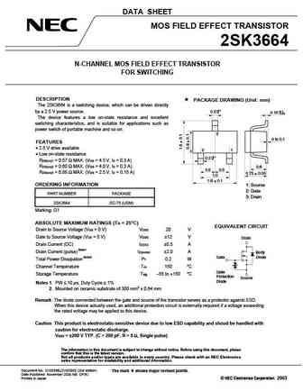
DATA SHEET MOS FIELD EFFECT TRANSISTOR 2SK3664 N-CHANNEL MOS FIELD EFFECT TRANSISTOR FOR SWITCHING DESCRIPTION PACKAGE DRAWING (Unit mm) The 2SK3664 is a switching device, which can be driven directly by a 2.5 V power source. 0.3 +0.1 0 0.15+0.1 0.05 The device features a low on-state resistance and excellent switching characteristics, and is suitable for applicat
2sk3663.pdf
DATA SHEET MOS FIELD EFFECT TRANSISTOR 2SK3663 N-CHANNEL MOS FIELD EFFECT TRANSISTOR FOR SWITCHING DESCRIPTION PACKAGE DRAWING (Unit mm) The 2SK3663 is a switching device which can be driven directly by a 2.5 V power source. The 2SK3663 features a low on-state resistance and excellent switching characteristics, and is suitable for applications such as power switch of portable machi
2sk3642.pdf
DATA SHEET MOS FIELD EFFECT TRANSISTOR 2SK3642 SWITCHING N-CHANNEL POWER MOS FET ORDERING INFORMATION DESCRIPTION The 2SK3642 is N-channel MOS FET device that features a low PART NUMBER PACKAGE on-state resistance and excellent switching characteristics, and 2SK3642-ZK TO-252 (MP-3ZK) designed for low voltage high current applications such as DC/DC converter with synchronou
2sk3668.pdf
DATA SHEET MOS FIELD EFFECT TRANSISTOR 2SK3668 SWITCHING N-CHANNEL POWER MOS FET DESCRIPTION ORDERING INFORMATION The 2SK3668 is N-channel DMOS FET device that PART NUMBER PACKAGE features a low on-state resistance, low charge and excellent switching characteristics, designed for high 2SK3668-ZK TO-263 (MP-25ZK) voltage applications such as high intensity discharge lamp drive. (T
2sk3666.pdf
Ordering number EN8158B 2SK3666 N-Channel JFET http //onsemi.com 30V, 0.6 to 6.0mA, 6.5mS, CP Applications Low-frequency general-purpose amplifier, impedance conversion, infrared sensor applications Features Small IGSS Small Ciss Specifications Absolute Maximum Ratings at Ta=25 C Parameter Symbol Conditions Ratings Unit Drain-to-Source Voltage VDSX 30 V Gate-to-Drai
2sk3637.pdf
www.DataSheet4U.com Power MOSFETs 2SK3637 Silicon N-channel power MOSFET Unit mm 15.5 0.5 3.0 0.3 3.2 0.1 5 For PDP/For high-speed switching 5 Features Low on-resistance, low Qg 5 High avalanche resistance 5 (4.0) 5 2.0 0.2 Absolute Maximum Ratings TC = 25 C 1.1 0.1 0.7 0.1 Parameter Symbol Rating Unit 5.45 0.3 Drain-source surrender
2sk3601-01.pdf
2SK3601-01 200304 FUJI POWER MOSFET N-CHANNEL SILICON POWER MOSFET Outline Drawings (mm) Super FAP-G Series Features High speed switching Low on-resistance No secondary breadown Low driving power Avalanche-proof Applications Switching regulators UPS (Uninterruptible Power Supply) DC-DC converters Maximum ratings and characteristic Foot Print Pattern Absolute maximum ratings
2sk3684-01l-01s-01sj.pdf
2SK3684-01L,S,SJ 200309 FUJI POWER MOSFET N-CHANNEL SILICON POWER MOSFET Super FAP-G Series Outline Drawings [mm] Features High speed switching Low on-resistance No secondary breadown Low driving power Avalanche-proof Applications P4 Switching regulators DC-DC converters UPS (Uninterruptible Power Supply) Maximum ratings and characteristicAbsolute maximum ratings (Tc=25 C
2sk3612-01l-s-sj.pdf
2SK3612-01L,S,SJ 200304 FUJI POWER MOSFET N-CHANNEL SILICON POWER MOSFET Super FAP-G Series Outline Drawings (mm) Features High speed switching Low on-resistance No secondary breadown Low driving power Avalanche-proof Applications P4 Switching regulators UPS (Uninterruptible Power Supply) DC-DC converters Maximum ratings and characteristicAbsolute maximum ratings (Tc=25 C unl
2sk3696-01mr.pdf
2SK3696-01MR 200309 FUJI POWER MOSFET N-CHANNEL SILICON POWER MOSFET Super FAP-G Series Outline Drawings [mm] Features TO-220F High speed switching Low on-resistance No secondary breadown Low driving power Avalanche-proof Applications Switching regulators DC-DC converters UPS (Uninterruptible Power Supply) Maximum ratings and characteristicAbsolute maximum ratings (Tc=25 C
2sk3697-01.pdf
2SK3697-01 N-CHANNEL SILICON POWER MOSFET 200407 Outline Drawings (mm) FUJI POWER MOSFET Super FAP-G Series Features High speed switching Low on-resistance No secondary breakdown Low driving power Avalanche-proof Applications Switching regulators DC-DC converters UPS (Uninterruptible Power Supply) Maximum ratings and characteristic Absolute maximum ratings (Tc=25 C unless
2sk3648-01.pdf
2SK3648-01 200304 FUJI POWER MOSFET N-CHANNEL SILICON POWER MOSFET Outline Drawings [mm] Super FAP-G Series TO-220AB Features High speed switching Low on-resistance No secondary breadown Low driving power Avalanche-proof Applications Switching regulators UPS (Uninterruptible Power Supply) DC-DC converters Maximum ratings and characteristicAbsolute maximum ratings (Tc=25 C unl
2sk3677-01mr.pdf

2SK3677-01MR 200304 FUJI POWER MOSFET N-CHANNEL SILICON POWER MOSFET Outline Drawings [mm] Super FAP-G Series TO-220F Features High speed switching Low on-resistance No secondary breadown Low driving power Avalanche-proof Applications Switching regulators UPS (Uninterruptible Power Supply) DC-DC converters Maximum ratings and characteristicAbsolute maximum ratings (Tc=25 C un
2sk3694-01l-s-sj.pdf
2SK3694-01L,S,SJ 200305 FUJI POWER MOSFET N-CHANNEL SILICON POWER MOSFET Super FAP-G Series Outline Drawings [mm] T-Pack Features High speed switching Low on-resistance No secondary breadown Low driving power Avalanche-proof P4 Applications Switching regulators UPS (Uninterruptible Power Supply) DC-DC converters Maximum ratings and characteristicAbsolute maximum ratings (Tc=25
2sk3681-01.pdf
2SK3681-01 200401 FUJI POWER MOSFET N-CHANNEL SILICON POWER MOSFET Super FAP-G Series Outline Drawings [mm] Features High speed switching Low on-resistance 11.6 0.2 No secondary breadown Low driving power Avalanche-proof Applications Switching regulators DC-DC converters UPS (Uninterruptible Power Supply) Maximum ratings and characteristicAbsolute maximum ratings (Tc=25 C
2sk3683-01mr.pdf
2SK3683-01MR 200309 FUJI POWER MOSFET N-CHANNEL SILICON POWER MOSFET Super FAP-G Series Outline Drawings [mm] Features TO-220F High speed switching Low on-resistance No secondary breadown Low driving power Avalanche-proof Applications Switching regulators DC-DC converters UPS (Uninterruptible Power Supply) Maximum ratings and characteristicAbsolute maximum ratings (Tc=25 C
2sk3608-01l-s-sj.pdf
2SK3608-01L,S,SJ 200304 FUJI POWER MOSFET N-CHANNEL SILICON POWER MOSFET Super FAP-G Series Outline Drawings (mm) Features High speed switching Low on-resistance No secondary breadown Low driving power Avalanche-proof P4 Applications Switching regulators UPS (Uninterruptible Power Supply) DC-DC converters Maximum ratings and characteristicAbsolute maximum ratings (Tc=25 C unl
2sk3673-01mr.pdf

2SK3673-01MR 200304 FUJI POWER MOSFET N-CHANNEL SILICON POWER MOSFET Outline Drawings [mm] Super FAP-G Series TO-220F Features High speed switching Low on-resistance No secondary breadown Low driving power Avalanche-proof Applications Switching regulators UPS (Uninterruptible Power Supply) DC-DC converters Maximum ratings and characteristicAbsolute maximum ratings (Tc=25 C un
2sk3651-01r.pdf

2SK3651-01R [0311] FUJI POWER MOSFET N-CHANNEL SILICON POWER MOSFET Super FAP-G Series Outline Drawings (mm) Features TO-3PF High speed switching Low on-resistance No secondary breadown Low driving power Avalanche-proof Applications Switching regulators UPS (Uninterruptible Power Supply) DC-DC converters Maximum ratings and characteristicAbsolute maximum ratings (Tc=25 C unle
2sk3692-01.pdf

2SK3692-01 200305 FUJI POWER MOSFET N-CHANNEL SILICON POWER MOSFET Super FAP-G Series Outline Drawings [mm] TO-220AB Features High speed switching Low on-resistance No secondary breadown Low driving power Avalanche-proof Applications Switching regulators UPS (Uninterruptible Power Supply) DC-DC converters Maximum ratings and characteristicAbsolute maximum ratings (Tc=25 C unle
2sk3685-01.pdf

2SK3685-01 200401 FUJI POWER MOSFET N-CHANNEL SILICON POWER MOSFET Super FAP-G Series Outline Drawings [mm] Features High speed switching Low on-resistance 11.6 0.2 No secondary breadown Low driving power Avalanche-proof Applications Switching regulators DC-DC converters UPS (Uninterruptible Power Supply) Maximum ratings and characteristicAbsolute maximum ratings (Tc=25 C
2sk3606-01.pdf

2SK3606-01 200304 FUJI POWER MOSFET N-CHANNEL SILICON POWER MOSFET Super FAP-G Series Outline Drawings (mm) Features TO-220AB High speed switching Low on-resistance No secondary breadown Low driving power Avalanche-proof Applications Switching regulators UPS (Uninterruptible Power Supply) DC-DC converters Maximum ratings and characteristicAbsolute maximum ratings (Tc=25 C unl
2sk3688-01l-01s-01sj.pdf
2SK3688-01L,S,SJ FUJI POWER MOSFET 200509 N-CHANNEL SILICON POWER MOSFET Super FAP-G Series Features Outline Drawings [mm] High speed switching Low on-resistance No secondary breadown Low driving power P4 Avalanche-proof Applications Switching regulators UPS (Uninterruptible Power Supply) DC-DC converters Maximum ratings and characteristicAbsolute maximum ratings (Tc=25 C unle
2sk3695-01.pdf
2SK3695-01 200309 FUJI POWER MOSFET N-CHANNEL SILICON POWER MOSFET Super FAP-G Series Outline Drawings [mm] Features TO-220AB High speed switching Low on-resistance No secondary breadown Low driving power Avalanche-proof Applications Switching regulators DC-DC converters UPS (Uninterruptible Power Supply) Maximum ratings and characteristicAbsolute maximum ratings (Tc=25 C
2sk3686-01.pdf
FUJI POWER MOSFET 2SK3686-01 200509 N-CHANNEL SILICON POWER MOSFET Super FAP-G Series Outline Drawings [mm] Features TO-220AB High speed switching Low on-resistance No secondary breadown Low driving power Avalanche-proof Applications Switching regulators UPS (Uninterruptible Power Supply) DC-DC converters Maximum ratings and characteristicAbsolute maximum ratings (Tc=25 C unl
2sk3680-01.pdf
2SK3680-01 200401 FUJI POWER MOSFET N-CHANNEL SILICON POWER MOSFET Super FAP-G Series Outline Drawings [mm] Features High speed switching Low on-resistance 11.6 0.2 No secondary breadown Low driving power Avalanche-proof Applications Switching regulators DC-DC converters UPS (Uninterruptible Power Supply) Maximum ratings and characteristicAbsolute maximum ratings (Tc=25 C
2sk3650-01l-s-sj.pdf
2SK3650-01L,S,SJ 200304 FUJI POWER MOSFET N-CHANNEL SILICON POWER MOSFET Outline Drawings [mm] Super FAP-G Series Features High speed switching Low on-resistance No secondary breadown Low driving power Avalanche-proof Applications P4 Switching regulators UPS (Uninterruptible Power Supply) DC-DC converters Maximum ratings and characteristicAbsolute maximum ratings (Tc=25 C unl
2sk3690-01.pdf
2SK3690-01 N-CHANNEL SILICON POWER MOSFET Outline Drawings (mm) 200406 TO-220AB FUJI POWER MOSFET Super FAP-G Series Features High speed switching Low on-resistance No secondary breakdown Low driving power Avalanche-proof Applications Switching regulators DC-DC converters UPS (Uninterruptible Power Supply) Maximum ratings and characteristic Absolute maximum ratings (Tc=25 C
2sk3609-01.pdf
2SK3609-01 200304 FUJI POWER MOSFET N-CHANNEL SILICON POWER MOSFET Outline Drawings (mm) Super FAP-G Series Features High speed switching Low on-resistance No secondary breadown Low driving power Avalanche-proof Applications Switching regulators UPS (Uninterruptible Power Supply) DC-DC converters Maximum ratings and characteristic Absolute maximum ratings Foot Print Pattern (
2sk3611-01mr.pdf
2SK3611-01MR 200304 FUJI POWER MOSFET N-CHANNEL SILICON POWER MOSFET Super FAP-G Series Outline Drawings (mm) Features TO-220F High speed switching Low on-resistance No secondary breadown Low driving power Avalanche-proof Applications Switching regulators UPS (Uninterruptible Power Supply) DC-DC converters Maximum ratings and characteristicAbsolute maximum ratings (Tc=25 C un
2sk3649-01mr.pdf
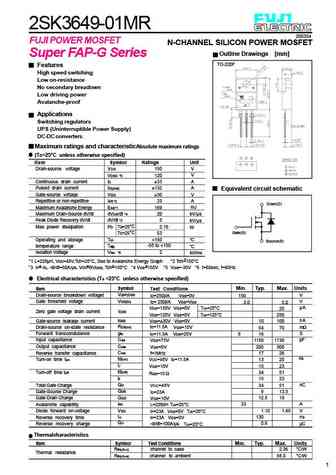
2SK3649-01MR 200304 FUJI POWER MOSFET N-CHANNEL SILICON POWER MOSFET Outline Drawings [mm] Super FAP-G Series TO-220F Features High speed switching Low on-resistance No secondary breadown Low driving power Avalanche-proof Applications Switching regulators UPS (Uninterruptible Power Supply) DC-DC converters Maximum ratings and characteristicAbsolute maximum ratings (Tc=25 C un
2sk3646-01l-s-sj.pdf

2SK3646-01L,S,SJ 200304 FUJI POWER MOSFET N-CHANNEL SILICON POWER MOSFET Super FAP-G Series Outline Drawings (mm) Features High speed switching Low on-resistance No secondary breadown Low driving power Avalanche-proof P4 Applications Switching regulators UPS (Uninterruptible Power Supply) DC-DC converters Maximum ratings and characteristicAbsolute maximum ratings (Tc=25 C unl
2sk3603-01mr.pdf
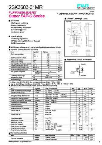
2SK3603-01MR 200304 FUJI POWER MOSFET N-CHANNEL SILICON POWER MOSFET Super FAP-G Series Outline Drawings (mm) Features TO-220F High speed switching Low on-resistance No secondary breadown Low driving power Avalanche-proof Applications Switching regulators UPS (Uninterruptible Power Supply) DC-DC converters Maximum ratings and characteristicAbsolute maximum ratings (Tc=25 C un
2sk3691-01mr.pdf
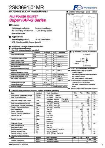
2SK3691-01MR N-CHANNEL SILICON POWER MOSFET Outline Drawings (mm) 200406 TO-220F FUJI POWER MOSFET Super FAP-G Series Features High speed switching Low on-resistance No secondary breakdown Low driving power Avalanche-proof Applications Switching regulators DC-DC converters UPS (Uninterruptible Power Supply) Maximum ratings and characteristic Absolute maximum ratings (Tc=25
2sk3647-01.pdf
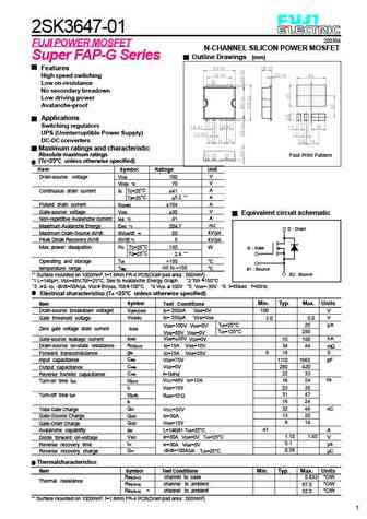
2SK3647-01 200304 FUJI POWER MOSFET N-CHANNEL SILICON POWER MOSFET Outline Drawings (mm) Super FAP-G Series Features High speed switching Low on-resistance No secondary breadown Low driving power Avalanche-proof Applications Switching regulators UPS (Uninterruptible Power Supply) DC-DC converters Maximum ratings and characteristic Absolute maximum ratings Foot Print Pattern (
2sk3607-01mr.pdf

2SK3607-01MR 200304 FUJI POWER MOSFET N-CHANNEL SILICON POWER MOSFET Super FAP-G Series Outline Drawings (mm) Features TO-220F High speed switching Low on-resistance No secondary breadown Low driving power Avalanche-proof Applications Switching regulators UPS (Uninterruptible Power Supply) DC-DC converters Maximum ratings and characteristicAbsolute maximum ratings (Tc=25 C un
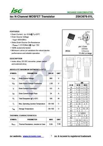
2sk3676-01l-01s-01sj.pdf

2SK3676-01L,S,SJ 200304 FUJI POWER MOSFET N-CHANNEL SILICON POWER MOSFET Outline Drawings [mm] Super FAP-G Series Features High speed switching Low on-resistance No secondary breadown Low driving power Avalanche-proof Applications P4 Switching regulators UPS (Uninterruptible Power Supply) DC-DC converters Maximum ratings and characteristicAbsolute maximum ratings (Tc=25 C unl
2sk3611.pdf

2SK3611-01MR FUJI POWER MOSFET N-CHANNEL SILICON POWER MOSFET Super FAP-G Series Outline Drawings (mm) Features TO-220F High speed switching Low on-resistance No secondary breadown Low driving power Avalanche-proof Applications Switching regulators UPS (Uninterruptible Power Supply) DC-DC converters Maximum ratings and characteristicAbsolute maximum ratings (Tc=25 C unless oth
2sk3644-01.pdf
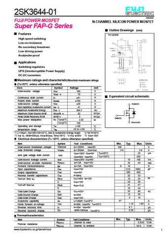
2SK3644-01 200304 FUJI POWER MOSFET N-CHANNEL SILICON POWER MOSFET Super FAP-G Series Outline Drawings (mm) Features TO-220AB High speed switching Low on-resistance No secondary breadown Low driving power Avalanche-proof Applications Switching regulators UPS (Uninterruptible Power Supply) DC-DC converters Maximum ratings and characteristicAbsolute maximum ratings (Tc=25 C unl
2sk3687-01mr.pdf
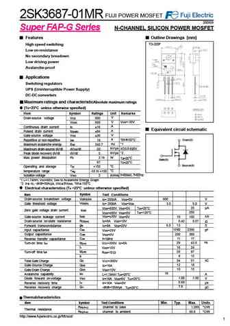
FUJI POWER MOSFET 2SK3687-01MR 200509 N-CHANNEL SILICON POWER MOSFET Super FAP-G Series Features Outline Drawings [mm] TO-220F High speed switching Low on-resistance No secondary breadown Low driving power Avalanche-proof Applications Switching regulators UPS (Uninterruptible Power Supply) DC-DC converters Maximum ratings and characteristicAbsolute maximum ratings (Tc=25 C unl
2sk3699-01mr.pdf

2SK3699-01MR 200305 FUJI POWER MOSFET N-CHANNEL SILICON POWER MOSFET Super FAP-G Series Outline Drawings [mm] Features TO-220F High speed switching Low on-resistance No secondary breadown Low driving power Avalanche-proof Applications Switching regulators UPS (Uninterruptible Power Supply) DC-DC converters Maximum ratings and characteristicAbsolute maximum ratings (Tc=25 C unl
2sk3645-01mr.pdf

2SK3645-01MR 200304 FUJI POWER MOSFET N-CHANNEL SILICON POWER MOSFET Super FAP-G Series Outline Drawings (mm) Features TO-220F High speed switching Low on-resistance No secondary breadown Low driving power Avalanche-proof Applications Switching regulators UPS (Uninterruptible Power Supply) DC-DC converters Maximum ratings and characteristicAbsolute maximum ratings (Tc=25 C un
2sk3610-01.pdf
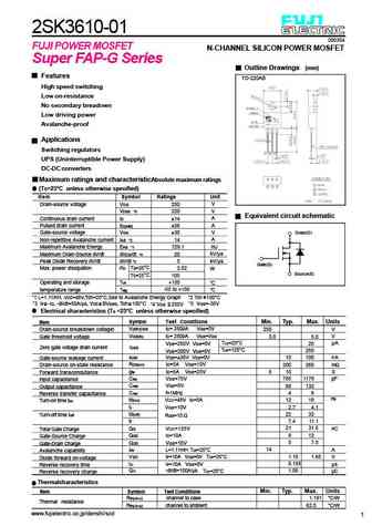
2SK3610-01 200304 FUJI POWER MOSFET N-CHANNEL SILICON POWER MOSFET Super FAP-G Series Outline Drawings (mm) Features TO-220AB High speed switching Low on-resistance No secondary breadown Low driving power Avalanche-proof Applications Switching regulators UPS (Uninterruptible Power Supply) DC-DC converters Maximum ratings and characteristicAbsolute maximum ratings (Tc=25 C unl
2sk3674-01l-s-sj.pdf

2SK3674-01L,S,SJ 200304 FUJI POWER MOSFET N-CHANNEL SILICON POWER MOSFET Outline Drawings [mm] Super FAP-G Series Features High speed switching Low on-resistance No secondary breadown Low driving power Avalanche-proof Applications P4 Switching regulators UPS (Uninterruptible Power Supply) DC-DC converters Maximum ratings and characteristicAbsolute maximum ratings (Tc=25 C unl
2sk3689-01.pdf
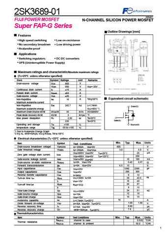
2SK3689-01 200401 FUJI POWER MOSFET N-CHANNEL SILICON POWER MOSFET Super FAP-G Series Outline Drawings [mm] Features High speed switching Low on-resistance 11.6 0.2 No secondary breadown Low driving power Avalanche-proof Applications Switching regulators DC-DC converters UPS (Uninterruptible Power Supply) Maximum ratings and characteristicAbsolute maximum ratings (Tc=25 C
2sk3693-01mr.pdf
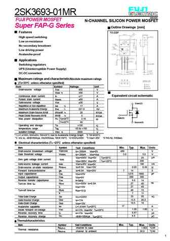
2SK3693-01MR 200305 FUJI POWER MOSFET N-CHANNEL SILICON POWER MOSFET Super FAP-G Series Outline Drawings [mm] Features TO-220F High speed switching Low on-resistance No secondary breadown Low driving power Avalanche-proof Applications Switching regulators UPS (Uninterruptible Power Supply) DC-DC converters Maximum ratings and characteristicAbsolute maximum ratings (Tc=25 C un
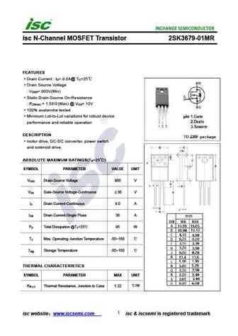
2sk3679-01mr.pdf

2SK3679-01MR 200304 FUJI POWER MOSFET N-CHANNEL SILICON POWER MOSFET Super FAP-G Series Outline Drawings [mm] TO-220F Features High speed switching Low on-resistance No secondary breadown Low driving power Avalanche-proof Applications Switching regulators UPS (Uninterruptible Power Supply) DC-DC converters Maximum ratings and characteristicAbsolute maximum ratings (Tc=25 C unl
2sk3682-01.pdf
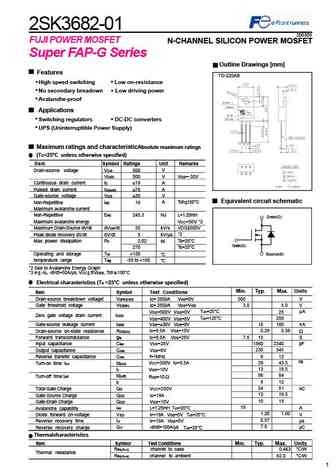
2SK3682-01 200309 FUJI POWER MOSFET N-CHANNEL SILICON POWER MOSFET Super FAP-G Series Outline Drawings [mm] Features TO-220AB High speed switching Low on-resistance No secondary breadown Low driving power Avalanche-proof Applications Switching regulators DC-DC converters UPS (Uninterruptible Power Supply) Maximum ratings and characteristicAbsolute maximum ratings (Tc=25 C
2sk3613-01.pdf
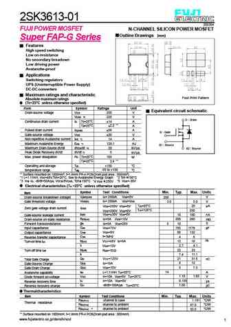
2SK3613-01 200304 FUJI POWER MOSFET N-CHANNEL SILICON POWER MOSFET Outline Drawings (mm) Super FAP-G Series Features High speed switching Low on-resistance No secondary breadown Low driving power Avalanche-proof Applications Switching regulators UPS (Uninterruptible Power Supply) DC-DC converters Maximum ratings and characteristic Foot Print Pattern Absolute maximum ratings (
2sk3605-01.pdf
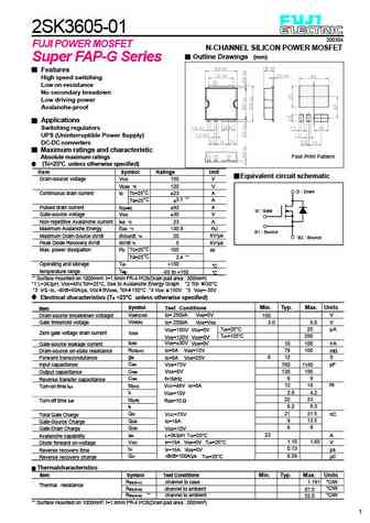
2SK3605-01 200304 FUJI POWER MOSFET N-CHANNEL SILICON POWER MOSFET Outline Drawings (mm) Super FAP-G Series Features High speed switching Low on-resistance No secondary breadown Low driving power Avalanche-proof Applications Switching regulators UPS (Uninterruptible Power Supply) DC-DC converters Maximum ratings and characteristic Absolute maximum ratings Foot Print Pattern (
2sk3600-01l-s-sj.pdf
2SK3600-01L,S,SJ 200304 FUJI POWER MOSFET N-CHANNEL SILICON POWER MOSFET Super FAP-G Series Outline Drawings (mm) Features High speed switching Low on-resistance No secondary breadown Low driving power Avalanche-proof P4 Applications Switching regulators UPS (Uninterruptible Power Supply) DC-DC converters Maximum ratings and characteristicAbsolute maximum ratings (Tc=25 C unl
2sk3678-01.pdf
2SK3678-01 200304 FUJI POWER MOSFET N-CHANNEL SILICON POWER MOSFET Super FAP-G Series Outline Drawings [mm] TO-220AB Features High speed switching Low on-resistance No secondary breadown Low driving power Avalanche-proof Applications Switching regulators UPS (Uninterruptible Power Supply) DC-DC converters Maximum ratings and characteristicAbsolute maximum ratings (Tc=25 C unle
2sk3675-01.pdf

2SK3675-01 200401 FUJI POWER MOSFET N-CHANNEL SILICON POWER MOSFET Outline Drawings [mm] Super FAP-G Series Features High speed switching 11.6 0.2 Low on-resistance No secondary breadown Low driving power Avalanche-proof Applications Switching regulators UPS (Uninterruptible Power Supply) DC-DC converters Maximum ratings and characteristicAbsolute maximum ratings (Tc=25 C un
2sk3698-01.pdf

2SK3698-01 200305 FUJI POWER MOSFET N-CHANNEL SILICON POWER MOSFET Super FAP-G Series Outline Drawings [mm] TO-220AB Features High speed switching Low on-resistance No secondary breadown Low driving power Avalanche-proof Applications Switching regulators UPS (Uninterruptible Power Supply) DC-DC converters Maximum ratings and characteristicAbsolute maximum ratings (Tc=25 C unle
2sk3604-01l-s-sj.pdf

2SK3604-01L,S,SJ 200304 FUJI POWER MOSFET N-CHANNEL SILICON POWER MOSFET Super FAP-G Series Outline Drawings (mm) Features High speed switching Low on-resistance No secondary breadown Low driving power Avalanche-proof P4 Applications Switching regulators UPS (Uninterruptible Power Supply) DC-DC converters Maximum ratings and characteristicAbsolute maximum ratings (Tc=25 C unl
2sk3602-01.pdf

2SK3602-01 200304 FUJI POWER MOSFET N-CHANNEL SILICON POWER MOSFET Super FAP-G Series Outline Drawings (mm) Features TO-220AB High speed switching Low on-resistance No secondary breadown Low driving power Avalanche-proof Applications Switching regulators UPS (Uninterruptible Power Supply) DC-DC converters Maximum ratings and characteristicAbsolute maximum ratings (Tc=25 C unl
2sk113 2sk152 2sk363 2sj44 ifn113 ifn152 ifn363 ifp44.pdf
Databook.fxp 1/13/99 2 09 PM Page D-3 01/99 D-3 Japanese Equivalent JFET Types Silicon Junction Field-Effect Transistors 2SK113 2SK152 2SK363 2SJ44 Japanese IFN113 IFN152 IFN363 IFP44 InterFET NJ132 NJ132L NJ450 PJ99 Process N N N P Unit Channel Channel Channel Channel Limit Parameters V 50 20 40 25 BVGSS Min 1.0 0.1 1.0 1.0 nA IGSS ( 20 V) ( 10 V) ( 30 V) (
2sk3643.pdf
SMD Type IC SMD Type Transistors SMD Type SMD Type SMD Type SMD Type SMD Type SMD Type SMD Type SMD Type SMD Type SMD Type SMD Type IC SMD Type IC Product specification 2SK3643 TO-252 Unit mm +0.1 6.50+0.15 2.30-0.1 -0.15 Features +0.8 5.30+0.2 0.50-0.7 -0.2 Low on-state resistance RDS(on)1 =6 m MAX. (VGS =10 V, ID =32A) RDS(on)2 =9 m MAX. (VGS =4.5 V, ID =32 A) 0.12
2sk3641.pdf
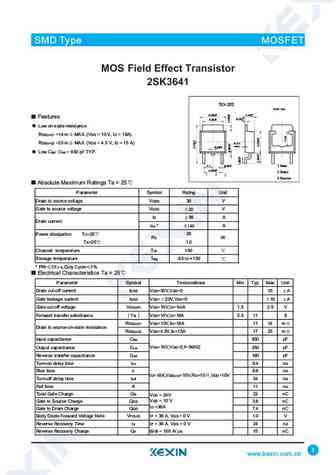
SMD Type IC SMD Type MOSFET MOS Field Effect Transistor 2SK3641 TO-252 Unit mm +0.1 6.50+0.15 2.30-0.1 -0.15 Features +0.8 5.30+0.2 0.50-0.7 -0.2 Low on-state resistance RDS(on)1 =14 m MAX. (VGS =10 V, ID =18A) 0.127 RDS(on)2 =25 m MAX. (VGS =4.5 V, ID =15 A) 0.80+0.1 max -0.1 Low Ciss Ciss = 930 pF TYP. 2.3 0.60+0.1 1Gate -0.1 +0.15 4.60-0.15 2Drain 3Source Absolute
2sk3640.pdf
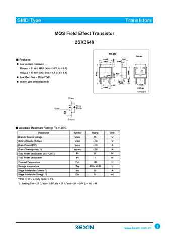
SMD Type IC SMD Type Transistors MOS Field Effect Transistor 2SK3640 TO-252 Unit mm 6.50+0.15 2.30+0.1 -0.15 -0.1 Features +0.2 5.30-0.2 0.50+0.8 -0.7 Low on-state resistance RDS(on)1 =21m MAX. (VGS =10 V, ID =9A) RDS(on)2 =40m MAX. (VGS =4.5 V, ID =9 A) 0.127 0.80+0.1 max -0.1 Low Ciss Ciss = 570 pF TYP. Built-in gate protection diode 1. Gate 2.3 0.60+0.1 -0.1 4.60+0.1
2sk3638.pdf

SMD Type IC SMD Type MOSFET MOS Field Effect Transistor 2SK3638 TO-252 Unit mm Features +0.15 +0.1 6.50-0.15 2.30-0.1 5.30+0.2 0.50+0.8 -0.2 -0.7 Low on-state resistance RDS(on)1 =8.5 m MAX. (VGS =10 V, ID =32A) RDS(on)2 =15 m MAX. (VGS =4.5 V, ID =18A) 0.127 Low Ciss Ciss = 1100 pF TYP. 0.80+0.1 max -0.1 Built-in gate protection diode +0.1 2.3 0.60-0.1 1Gate 4.60+0.15 -0
2sk3639.pdf
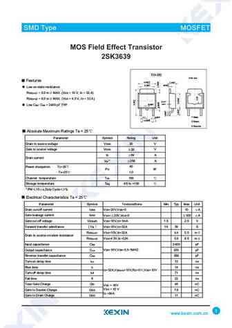
SMD Type IC SMD Type MOSFET MOS Field Effect Transistor 2SK3639 TO-252 Unit mm Features +0.15 +0.1 6.50-0.15 2.30-0.1 5.30+0.2 0.50+0.8 -0.2 -0.7 Low on-state resistance RDS(on)1 =5.5 m MAX. (VGS =10 V, ID =32A) RDS(on)2 =8.5 m MAX. (VGS =4.5 V, ID =32 A) 0.127 0.80+0.1 max -0.1 Low Ciss Ciss = 2400 pF TYP. +0.1 2.3 0.60-0.1 1Gate 4.60+0.15 -0.15 2Drain 3Source Absolut
2sk3652.pdf
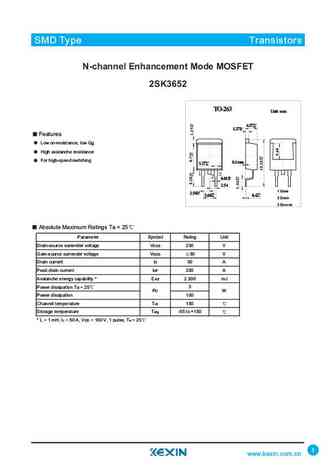
SMD Type IC SMD Type Transistors N-channel Enhancement Mode MOSFET 2SK3652 TO-263 Unit mm +0.2 4.57-0.2 1.27+0.1 -0.1 Features Low on-resistance, low Qg High avalanche resistance For high-speed switching 0.1max 1.27+0.1 -0.1 +0.1 0.81-0.1 2.54 1Gate 2.54+0.2 +0.2 -0.2 +0.1 5.08-0.1 0.4-0.2 2Drain 3 Source Absolute Maximum Ratings Ta = 25 Parameter Symbol Rating Unit
2sk3634.pdf
SMD Type IC SMD Type MOSFET MOS Field Effect Transistor 2SK3634 TO-252 Unit mm +0.15 +0.1 6.50-0.15 2.30-0.1 Features 5.30+0.2 0.50+0.8 -0.2 -0.7 High voltage VDSS = 200 V Gate voltage rating 30 V 0.127 RDS(on) =0.60 MAX. (VGS =10 V, ID =3.0 A) 0.80+0.1 max -0.1 Low Ciss Ciss = 270 pF TYP. (VDS =10 V, VGS =0V) Built-in gate protection diode +0.1 2.3 0.60-0.1 1Gate 4.60+
2sk3663.pdf
2SK3663 www.VBsemi.tw N-Channel 20 V (D-S) MOSFET FEATURES PRODUCT SUMMARY Halogen-free According to IEC 61249-2-21 VDS (V) RDS(on) ( )ID (A)a Qg (Typ.) Definition 0.036 at VGS = 10 V 4 TrenchFET Power MOSFET 20 0.040 at VGS = 4.5 V 3.8 4 nC Typical ESD Protection 2000 V HBM 0.048 at VGS = 2.5 V 3.6 100 % Rg Tested Compliant to RoHS Directive 2002/95/EC A
2sk3634.pdf
2SK3634 www.VBsemi.tw N-Channel 200 V (D-S) MOSFET FEATURES PRODUCT SUMMARY TrenchFET Power MOSFET VDS (V) RDS(on) ( )ID (A) 175 C Junction Temperature 200 0.245 at VGS = 10 V 10 PWM Optimized 100 % Rg Tested Compliant to RoHS Directive 2002/95/EC APPLICATIONS Primary Side Switch D TO-252 G S G D S N-Channel MOSFET ABSOLUTE MAXIMUM RATINGS
2sk3608l.pdf

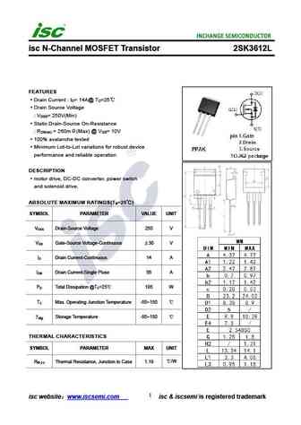
isc N-Channel MOSFET Transistor 2SK3608L FEATURES Drain Current I = 13A@ T =25 D C Drain Source Voltage V = 200V(Min) DSS Static Drain-Source On-Resistance R = 170m (Max) @ V = 10V DS(on) GS 100% avalanche tested Minimum Lot-to-Lot variations for robust device performance and reliable operation DESCRIPTION motor drive, DC-DC converter, power switch and solen
2sk3650-01sj.pdf
isc N-Channel MOSFET Transistor 2SK3650-01SJ FEATURES Drain Current I = 33A@ T =25 D C Drain Source Voltage V = 150V(Min) DSS Static Drain-Source On-Resistance R = 70m (Max) @ V = 10V DS(on) GS 100% avalanche tested Minimum Lot-to-Lot variations for robust device performance and reliable operation DESCRIPTION motor drive, DC-DC converter, power switch and so
2sk3646l.pdf

isc N-Channel MOSFET Transistor 2SK3646L FEATURES Drain Current I = 41A@ T =25 D C Drain Source Voltage V = 100V(Min) DSS Static Drain-Source On-Resistance R = 44m (Max) @ V = 10V DS(on) GS 100% avalanche tested Minimum Lot-to-Lot variations for robust device performance and reliable operation DESCRIPTION motor drive, DC-DC converter, power switch and soleno
2sk3634d.pdf
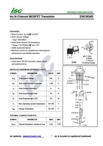
isc N-Channel MOSFET Transistor 2SK3634D FEATURES Drain Current I = 6A@ T =25 D C Drain Source Voltage V = 200V(Min) DSS Static Drain-Source On-Resistance R = 0.6 (Max) @ V = 10V DS(on) GS 100% avalanche tested Minimum Lot-to-Lot variations for robust device performance and reliable operation DESCRIPTION motor drive, DC-DC converter, power switch and solenoi
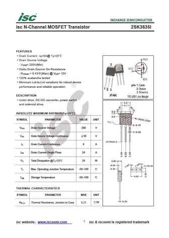
2sk3635d.pdf

isc N-Channel MOSFET Transistor 2SK3635D FEATURES Drain Current I =8A@ T =25 D C Drain Source Voltage V = 200V(Min) DSS Static Drain-Source On-Resistance R = 0.43 (Max) @ V = 10V DS(on) GS 100% avalanche tested Minimum Lot-to-Lot variations for robust device performance and reliable operation DESCRIPTION motor drive, DC-DC converter, power switch and solenoi
2sk3646s.pdf
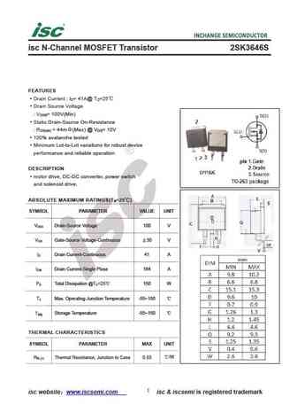
isc N-Channel MOSFET Transistor 2SK3646S FEATURES Drain Current I = 41A@ T =25 D C Drain Source Voltage V = 100V(Min) DSS Static Drain-Source On-Resistance R = 44m (Max) @ V = 10V DS(on) GS 100% avalanche tested Minimum Lot-to-Lot variations for robust device performance and reliable operation DESCRIPTION motor drive, DC-DC converter, power switch and soleno
2sk3688-01s.pdf

isc N-Channel MOSFET Transistor 2SK3688-01S FEATURES Drain Current I = 16A@ T =25 D C Drain Source Voltage V = 600V(Min) DSS Static Drain-Source On-Resistance R = 0.57 (Max) @ V = 10V DS(on) GS 100% avalanche tested Minimum Lot-to-Lot variations for robust device performance and reliable operation DESCRIPTION motor drive, DC-DC converter, power switch and so
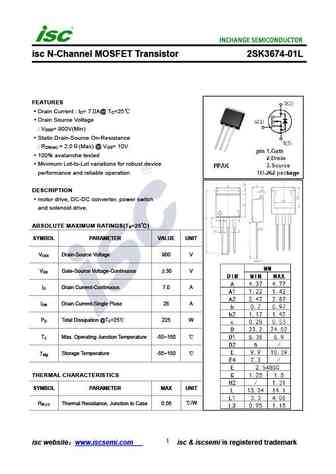
2sk3674-01s.pdf
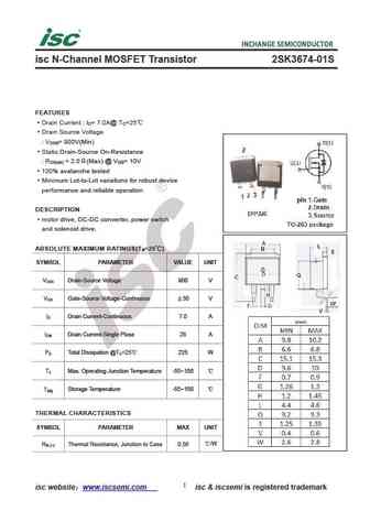
isc N-Channel MOSFET Transistor 2SK3674-01S FEATURES Drain Current I = 7.0A@ T =25 D C Drain Source Voltage V = 900V(Min) DSS Static Drain-Source On-Resistance R = 2.0 (Max) @ V = 10V DS(on) GS 100% avalanche tested Minimum Lot-to-Lot variations for robust device performance and reliable operation DESCRIPTION motor drive, DC-DC converter, power switch and so
2sk3604s.pdf

isc N-Channel MOSFET Transistor 2SK3604S FEATURES Drain Current I = 23A@ T =25 D C Drain Source Voltage V = 150V(Min) DSS Static Drain-Source On-Resistance R = 105m (Max) @ V = 10V DS(on) GS 100% avalanche tested Minimum Lot-to-Lot variations for robust device performance and reliable operation DESCRIPTION motor drive, DC-DC converter, power switch and solen
2sk3648-01.pdf

isc N-Channel MOSFET Transistor 2SK3648-01 FEATURES Drain Current I = 33A@ T =25 D C Drain Source Voltage V = 150V(Min) DSS Static Drain-Source On-Resistance R = 70m (Max) @ V = 10V DS(on) GS 100% avalanche tested Minimum Lot-to-Lot variations for robust device performance and reliable operation DESCRIPTION motor drive, DC-DC converter, power switch and sole
2sk3677-01mr.pdf
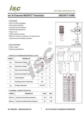
isc N-Channel MOSFET Transistor 2SK3677-01MR FEATURES With TO-220F packaging High speed switching Low gate input resistance Standard level gate drive Easy to use 100% avalanche tested Minimum Lot-to-Lot variations for robust device performance and reliable operation APPLICATIONS Power supply Switching applications ABSOLUTE MAXIMUM RATINGS(T =25 ) a SYMBO
2sk3634i.pdf

isc N-Channel MOSFET Transistor 2SK3634I FEATURES Drain Current I = 6A@ T =25 D C Drain Source Voltage V = 200V(Min) DSS Static Drain-Source On-Resistance R = 0.6 (Max) @ V = 10V DS(on) GS 100% avalanche tested Minimum Lot-to-Lot variations for robust device performance and reliable operation DESCRIPTION motor drive, DC-DC converter, power switch and solenoi
2sk3659.pdf
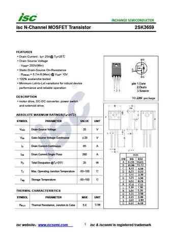
isc N-Channel MOSFET Transistor 2SK3659 FEATURES Drain Current I = 25A@ T =25 D C Drain Source Voltage V = 200V(Min) DSS Static Drain-Source On-Resistance R = 5.7m (Max) @ V = 10V DS(on) GS 100% avalanche tested Minimum Lot-to-Lot variations for robust device performance and reliable operation DESCRIPTION motor drive, DC-DC converter, power switch and soleno
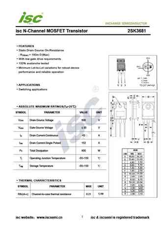
2sk3681-01.pdf
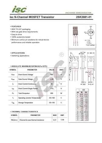
isc N-Channel MOSFET Transistor 2SK3681-01 FEATURES With TO-247 packaging With low gate drive requirements Easy to drive 100% avalanche tested Minimum Lot-to-Lot variations for robust device performance and reliable operation APPLICATIONS Switching applications ABSOLUTE MAXIMUM RATINGS(T =25 ) a SYMBOL PARAMETER VALUE UNIT V Drain-Source Voltage 600 V DSS V Ga
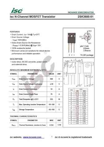
2sk3683-01mr.pdf

isc N-Channel MOSFET Transistor 2SK3683-01MR FEATURES Drain Current I = 19A@ T =25 D C Drain Source Voltage V = 500V(Min) DSS Static Drain-Source On-Resistance R = 0.38 (Max) @ V = 10V DS(on) GS 100% avalanche tested Minimum Lot-to-Lot variations for robust device performance and reliable operation DESCRIPTION motor drive, DC-DC converter, power switch and s
2sk3673-01mr.pdf

isc N-Channel MOSFET Transistor 2SK3673-01MR FEATURES Drain Current I = 10A@ T =25 D C Drain Source Voltage V = 700V(Min) DSS Static Drain-Source On-Resistance R = 1.18 (Max) @ V = 10V DS(on) GS 100% avalanche tested Minimum Lot-to-Lot variations for robust device performance and reliable operation DESCRIPTION motor drive, DC-DC converter, power switch and s
2sk3651-01r.pdf
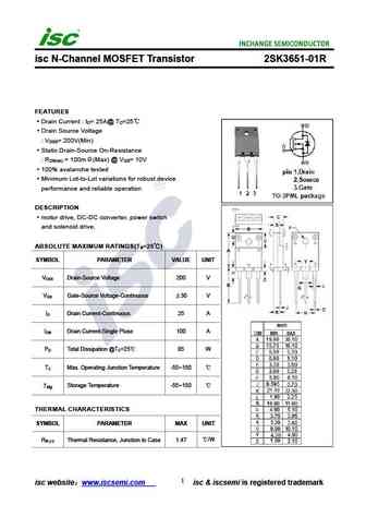
isc N-Channel MOSFET Transistor 2SK3651-01R FEATURES Drain Current I = 25A@ T =25 D C Drain Source Voltage V = 200V(Min) DSS Static Drain-Source On-Resistance R = 100m (Max) @ V = 10V DS(on) GS 100% avalanche tested Minimum Lot-to-Lot variations for robust device performance and reliable operation DESCRIPTION motor drive, DC-DC converter, power switch and so
2sk3692-01.pdf

isc N-Channel MOSFET Transistor 2SK3692-01 FEATURES Drain Current I = 17A@ T =25 D C Drain Source Voltage V = 450V(Min) DSS Static Drain-Source On-Resistance R = 0.38 (Max) @ V = 10V DS(on) GS 100% avalanche tested Minimum Lot-to-Lot variations for robust device performance and reliable operation DESCRIPTION motor drive, DC-DC converter, power switch and sol
2sk3685-01.pdf
isc N-Channel MOSFET Transistor 2SK3685-01 FEATURES Drain Current I = 19A@ T =25 D C Drain Source Voltage V = 500V(Min) DSS Static Drain-Source On-Resistance R = 0.38 (Max) @ V = 10V DS(on) GS 100% avalanche tested Minimum Lot-to-Lot variations for robust device performance and reliable operation DESCRIPTION motor drive, DC-DC converter, power switch and sol
2sk3612l.pdf
isc N-Channel MOSFET Transistor 2SK3612L FEATURES Drain Current I = 14A@ T =25 D C Drain Source Voltage V = 250V(Min) DSS Static Drain-Source On-Resistance R = 260m (Max) @ V = 10V DS(on) GS 100% avalanche tested Minimum Lot-to-Lot variations for robust device performance and reliable operation DESCRIPTION motor drive, DC-DC converter, power switch and solen
2sk3606-01.pdf
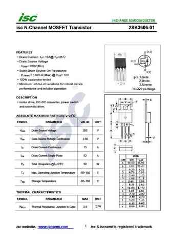
isc N-Channel MOSFET Transistor 2SK3606-01 FEATURES Drain Current I = 13A@ T =25 D C Drain Source Voltage V = 200V(Min) DSS Static Drain-Source On-Resistance R = 170m (Max) @ V = 10V DS(on) GS 100% avalanche tested Minimum Lot-to-Lot variations for robust device performance and reliable operation DESCRIPTION motor drive, DC-DC converter, power switch and sol
2sk3674-01l.pdf
isc N-Channel MOSFET Transistor 2SK3674-01L FEATURES Drain Current I = 7.0A@ T =25 D C Drain Source Voltage V = 900V(Min) DSS Static Drain-Source On-Resistance R = 2.0 (Max) @ V = 10V DS(on) GS 100% avalanche tested Minimum Lot-to-Lot variations for robust device performance and reliable operation DESCRIPTION motor drive, DC-DC converter, power switch and so
2sk3686-01.pdf

isc N-Channel MOSFET Transistor 2SK3686-01 FEATURES Drain Current I = 16A@ T =25 D C Drain Source Voltage V = 600V(Min) DSS Static Drain-Source On-Resistance R = 0.57 (Max) @ V = 10V DS(on) GS 100% avalanche tested Minimum Lot-to-Lot variations for robust device performance and reliable operation DESCRIPTION motor drive, DC-DC converter, power switch and sol
2sk3680.pdf
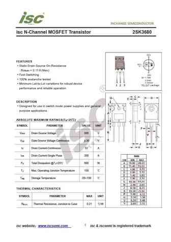
isc N-Channel MOSFET Transistor 2SK3680 FEATURES Static Drain-Source On-Resistance R = 0.11 (Max) DS(on) Fast Switching 100% avalanche tested Minimum Lot-to-Lot variations for robust device performance and reliable operation DESCRIPTION Designed for use in switch mode power supplies and general purpose applications. ABSOLUTE MAXIMUM RATINGS(T =25 ) a SYMBOL PARAMETE
2sk3635i.pdf
isc N-Channel MOSFET Transistor 2SK3635I FEATURES Drain Current I =8A@ T =25 D C Drain Source Voltage V = 200V(Min) DSS Static Drain-Source On-Resistance R = 0.43 (Max) @ V = 10V DS(on) GS 100% avalanche tested Minimum Lot-to-Lot variations for robust device performance and reliable operation DESCRIPTION motor drive, DC-DC converter, power switch and solenoi
2sk3615i.pdf

isc N-Channel MOSFET Transistor 2SK3615I FEATURES Drain Current I = 12A@ T =25 D C Drain Source Voltage V = 60V(Min) DSS Static Drain-Source On-Resistance R = 60m (Max) @ V = 10V DS(on) GS 100% avalanche tested Minimum Lot-to-Lot variations for robust device performance and reliable operation DESCRIPTION motor drive, DC-DC converter, power switch and solenoi
2sk3611-01mr.pdf

isc N-Channel MOSFET Transistor 2SK3611-01MR FEATURES Drain Current I = 10A@ T =25 D C Drain Source Voltage V = 250V(Min) DSS Static Drain-Source On-Resistance R = 260m (Max) @ V = 10V DS(on) GS 100% avalanche tested Minimum Lot-to-Lot variations for robust device performance and reliable operation DESCRIPTION motor drive, DC-DC converter, power switch and s
2sk3617d.pdf

isc N-Channel MOSFET Transistor 2SK3617D FEATURES Drain Current I = 6A@ T =25 D C Drain Source Voltage V = 100V(Min) DSS Static Drain-Source On-Resistance R = 225m (Max) @ V = 10V DS(on) GS 100% avalanche tested Minimum Lot-to-Lot variations for robust device performance and reliable operation DESCRIPTION motor drive, DC-DC converter, power switch and soleno
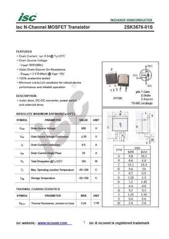
2sk3676-01sj.pdf

isc N-Channel MOSFET Transistor 2SK3676-01SJ FEATURES Drain Current I = 6.0A@ T =25 D C Drain Source Voltage V = 900V(Min) DSS Static Drain-Source On-Resistance R = 2.5 (Max) @ V = 10V DS(on) GS 100% avalanche tested Minimum Lot-to-Lot variations for robust device performance and reliable operation DESCRIPTION motor drive, DC-DC converter, power switch and s
2sk3649-01mr.pdf

isc N-Channel MOSFET Transistor 2SK3649-01MR FEATURES Drain Current I = 33A@ T =25 D C Drain Source Voltage V = 150V(Min) DSS Static Drain-Source On-Resistance R = 70m (Max) @ V = 10V DS(on) GS 100% avalanche tested Minimum Lot-to-Lot variations for robust device performance and reliable operation DESCRIPTION motor drive, DC-DC converter, power switch and so
2sk3694-01sj.pdf

isc N-Channel MOSFET Transistor 2SK3694-01SJ FEATURES Drain Current I = 17A@ T =25 D C Drain Source Voltage V = 450V(Min) DSS Static Drain-Source On-Resistance R = 0.38 (Max) @ V = 10V DS(on) GS 100% avalanche tested Minimum Lot-to-Lot variations for robust device performance and reliable operation DESCRIPTION motor drive, DC-DC converter, power switch and s
2sk3600s.pdf
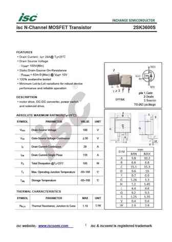
isc N-Channel MOSFET Transistor 2SK3600S FEATURES Drain Current I = 29A@ T =25 D C Drain Source Voltage V = 100V(Min) DSS Static Drain-Source On-Resistance R = 62m (Max) @ V = 10V DS(on) GS 100% avalanche tested Minimum Lot-to-Lot variations for robust device performance and reliable operation DESCRIPTION motor drive, DC-DC converter, power switch and soleno
2sk3681.pdf
isc N-Channel MOSFET Transistor 2SK3681 FEATURES Static Drain-Source On-Resistance R = 160m (Max) DS(on) With low gate drive requirements 100% avalanche tested Minimum Lot-to-Lot variations for robust device performance and reliable operation APPLICATIONS Switching applications ABSOLUTE MAXIMUM RATINGS(T =25 ) a SYMBOL PARAMETER VALUE UNIT V Drain-Source Volta
2sk3603-01mr.pdf

isc N-Channel MOSFET Transistor 2SK3603-01MR FEATURES Drain Current I = 23A@ T =25 D C Drain Source Voltage V = 150V(Min) DSS Static Drain-Source On-Resistance R = 105m (Max) @ V = 10V DS(on) GS 100% avalanche tested Minimum Lot-to-Lot variations for robust device performance and reliable operation DESCRIPTION motor drive, DC-DC converter, power switch and s
2sk3684-01l.pdf
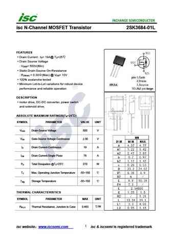
isc N-Channel MOSFET Transistor 2SK3684-01L FEATURES Drain Current I = 19A@ T =25 D C Drain Source Voltage V = 500V(Min) DSS Static Drain-Source On-Resistance R = 0.38 (Max) @ V = 10V DS(on) GS 100% avalanche tested Minimum Lot-to-Lot variations for robust device performance and reliable operation DESCRIPTION motor drive, DC-DC converter, power switch and so
2sk3607-01mr.pdf

isc N-Channel MOSFET Transistor 2SK3607-01MR FEATURES Drain Current I = 18A@ T =25 D C Drain Source Voltage V = 200V(Min) DSS Static Drain-Source On-Resistance R = 170m (Max) @ V = 10V DS(on) GS 100% avalanche tested Minimum Lot-to-Lot variations for robust device performance and reliable operation DESCRIPTION motor drive, DC-DC converter, power switch and s
2sk3650-01s.pdf

isc N-Channel MOSFET Transistor 2SK3650-01S FEATURES Drain Current I = 33A@ T =25 D C Drain Source Voltage V = 150V(Min) DSS Static Drain-Source On-Resistance R = 70m (Max) @ V = 10V DS(on) GS 100% avalanche tested Minimum Lot-to-Lot variations for robust device performance and reliable operation DESCRIPTION motor drive, DC-DC converter, power switch and sol
2sk3676-01s.pdf
isc N-Channel MOSFET Transistor 2SK3676-01S FEATURES Drain Current I = 6.0A@ T =25 D C Drain Source Voltage V = 900V(Min) DSS Static Drain-Source On-Resistance R = 2.5 (Max) @ V = 10V DS(on) GS 100% avalanche tested Minimum Lot-to-Lot variations for robust device performance and reliable operation DESCRIPTION motor drive, DC-DC converter, power switch and so
2sk3644-01.pdf
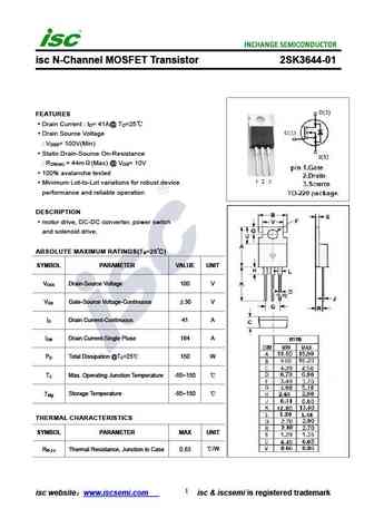
isc N-Channel MOSFET Transistor 2SK3644-01 FEATURES Drain Current I = 41A@ T =25 D C Drain Source Voltage V = 100V(Min) DSS Static Drain-Source On-Resistance R = 44m (Max) @ V = 10V DS(on) GS 100% avalanche tested Minimum Lot-to-Lot variations for robust device performance and reliable operation DESCRIPTION motor drive, DC-DC converter, power switch and sole
2sk3687-01mr.pdf

isc N-Channel MOSFET Transistor 2SK3687-01MR FEATURES Drain Current I = 16A@ T =25 D C Drain Source Voltage V = 600V(Min) DSS Static Drain-Source On-Resistance R = 0.57 (Max) @ V = 10V DS(on) GS 100% avalanche tested Minimum Lot-to-Lot variations for robust device performance and reliable operation DESCRIPTION motor drive, DC-DC converter, power switch and s
2sk3699-01mr.pdf

isc N-Channel MOSFET Transistor 2SK3699-01MR FEATURES Drain Current I = 3.7A@ T =25 D C Drain Source Voltage V = 900V(Min) DSS Static Drain-Source On-Resistance R = 4.3 (Max) @ V = 10V DS(on) GS 100% avalanche tested Minimum Lot-to-Lot variations for robust device performance and reliable operation DESCRIPTION motor drive, DC-DC converter, power switch and s
2sk3615d.pdf

isc N-Channel MOSFET Transistor 2SK3615D FEATURES Drain Current I = 12A@ T =25 D C Drain Source Voltage V = 60V(Min) DSS Static Drain-Source On-Resistance R = 60m (Max) @ V = 10V DS(on) GS 100% avalanche tested Minimum Lot-to-Lot variations for robust device performance and reliable operation DESCRIPTION motor drive, DC-DC converter, power switch and solenoi
2sk3645-01mr.pdf

isc N-Channel MOSFET Transistor 2SK3645-01MR FEATURES Drain Current I = 41A@ T =25 D C Drain Source Voltage V = 100V(Min) DSS Static Drain-Source On-Resistance R = 44m (Max) @ V = 10V DS(on) GS 100% avalanche tested Minimum Lot-to-Lot variations for robust device performance and reliable operation DESCRIPTION motor drive, DC-DC converter, power switch and so
2sk3618d.pdf

isc N-Channel MOSFET Transistor 2SK3618D FEATURES Drain Current I = 8A@ T =25 D C Drain Source Voltage V = 100V(Min) DSS Static Drain-Source On-Resistance R = 130m (Max) @ V = 10V DS(on) GS 100% avalanche tested Minimum Lot-to-Lot variations for robust device performance and reliable operation DESCRIPTION motor drive, DC-DC converter, power switch and soleno
2sk3610-01.pdf

isc N-Channel MOSFET Transistor 2SK3610-01 FEATURES Drain Current I = 14A@ T =25 D C Drain Source Voltage V = 250V(Min) DSS Static Drain-Source On-Resistance R = 260m (Max) @ V = 10V DS(on) GS 100% avalanche tested Minimum Lot-to-Lot variations for robust device performance and reliable operation DESCRIPTION motor drive, DC-DC converter, power switch and sol
2sk3608s.pdf
isc N-Channel MOSFET Transistor 2SK3608S FEATURES Drain Current I = 13A@ T =25 D C Drain Source Voltage V = 200V(Min) DSS Static Drain-Source On-Resistance R = 170m (Max) @ V = 10V DS(on) GS 100% avalanche tested Minimum Lot-to-Lot variations for robust device performance and reliable operation DESCRIPTION motor drive, DC-DC converter, power switch and solen
2sk3688-01sj.pdf

isc N-Channel MOSFET Transistor 2SK3688-01SJ FEATURES Drain Current I = 16A@ T =25 D C Drain Source Voltage V = 600V(Min) DSS Static Drain-Source On-Resistance R = 0.57 (Max) @ V = 10V DS(on) GS 100% avalanche tested Minimum Lot-to-Lot variations for robust device performance and reliable operation DESCRIPTION motor drive, DC-DC converter, power switch and s
2sk3612s.pdf
isc N-Channel MOSFET Transistor 2SK3612S FEATURES Drain Current I = 14A@ T =25 D C Drain Source Voltage V = 250V(Min) DSS Static Drain-Source On-Resistance R = 260m (Max) @ V = 10V DS(on) GS 100% avalanche tested Minimum Lot-to-Lot variations for robust device performance and reliable operation DESCRIPTION motor drive, DC-DC converter, power switch and solen
2sk3689-01.pdf

isc N-Channel MOSFET Transistor 2SK3689-01 FEATURES Drain Current I = 16A@ T =25 D C Drain Source Voltage V = 600V(Min) DSS Static Drain-Source On-Resistance R = 0.57 (Max) @ V = 10V DS(on) GS 100% avalanche tested Minimum Lot-to-Lot variations for robust device performance and reliable operation DESCRIPTION motor drive, DC-DC converter, power switch and sol
2sk3684-01s.pdf

isc N-Channel MOSFET Transistor 2SK3684-01S FEATURES Drain Current I = 19A@ T =25 D C Drain Source Voltage V = 500V(Min) DSS Static Drain-Source On-Resistance R = 0.38 (Max) @ V = 10V DS(on) GS 100% avalanche tested Minimum Lot-to-Lot variations for robust device performance and reliable operation DESCRIPTION motor drive, DC-DC converter, power switch and so
2sk3694-01l.pdf

isc N-Channel MOSFET Transistor 2SK3694-01L FEATURES Drain Current I = 17A@ T =25 D C Drain Source Voltage V = 450V(Min) DSS Static Drain-Source On-Resistance R = 0.38 (Max) @ V = 10V DS(on) GS 100% avalanche tested Minimum Lot-to-Lot variations for robust device performance and reliable operation DESCRIPTION motor drive, DC-DC converter, power switch and so
2sk3618i.pdf

isc N-Channel MOSFET Transistor 2SK3618I FEATURES Drain Current I = 8A@ T =25 D C Drain Source Voltage V = 100V(Min) DSS Static Drain-Source On-Resistance R = 130m (Max) @ V = 10V DS(on) GS 100% avalanche tested Minimum Lot-to-Lot variations for robust device performance and reliable operation DESCRIPTION motor drive, DC-DC converter, power switch and soleno
2sk3694-01s.pdf

isc N-Channel MOSFET Transistor 2SK3694-01S FEATURES Drain Current I = 17A@ T =25 D C Drain Source Voltage V = 450V(Min) DSS Static Drain-Source On-Resistance R = 0.38 (Max) @ V = 10V DS(on) GS 100% avalanche tested Minimum Lot-to-Lot variations for robust device performance and reliable operation DESCRIPTION motor drive, DC-DC converter, power switch and so
2sk3693-01mr.pdf

isc N-Channel MOSFET Transistor 2SK3693-01MR FEATURES Drain Current I = 17A@ T =25 D C Drain Source Voltage V = 450V(Min) DSS Static Drain-Source On-Resistance R = 0.38 (Max) @ V = 10V DS(on) GS 100% avalanche tested Minimum Lot-to-Lot variations for robust device performance and reliable operation DESCRIPTION motor drive, DC-DC converter, power switch and s
2sk3633.pdf
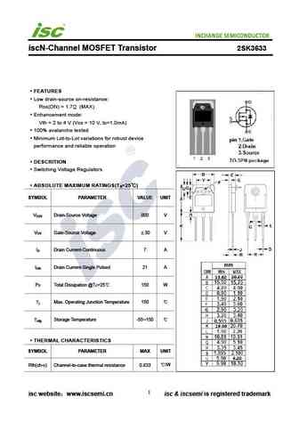
iscN-Channel MOSFET Transistor 2SK3633 FEATURES Low drain-source on-resistance RDS(ON) = 1.7 (MAX) Enhancement mode Vth = 2 to 4 V (VDS = 10 V, ID=1.0mA) 100% avalanche tested Minimum Lot-to-Lot variations for robust device performance and reliable operation DESCRITION Switching Voltage Regulators ABSOLUTE MAXIMUM RATINGS(T =25 ) a SYMBOL PARAMETER VALUE UNIT
2sk3679-01mr.pdf
isc N-Channel MOSFET Transistor 2SK3679-01MR FEATURES Drain Current I = 9.0A@ T =25 D C Drain Source Voltage V = 900V(Min) DSS Static Drain-Source On-Resistance R = 1.58 (Max) @ V = 10V DS(on) GS 100% avalanche tested Minimum Lot-to-Lot variations for robust device performance and reliable operation DESCRIPTION motor drive, DC-DC converter, power switch and
2sk3600l.pdf

isc N-Channel MOSFET Transistor 2SK3600L FEATURES Drain Current I = 29A@ T =25 D C Drain Source Voltage V = 100V(Min) DSS Static Drain-Source On-Resistance R = 62m (Max) @ V = 10V DS(on) GS 100% avalanche tested Minimum Lot-to-Lot variations for robust device performance and reliable operation DESCRIPTION motor drive, DC-DC converter, power switch and soleno
2sk3682-01.pdf

isc N-Channel MOSFET Transistor 2SK3682-01 FEATURES Drain Current I = 19A@ T =25 D C Drain Source Voltage V = 500V(Min) DSS Static Drain-Source On-Resistance R = 0.38 (Max) @ V = 10V DS(on) GS 100% avalanche tested Minimum Lot-to-Lot variations for robust device performance and reliable operation DESCRIPTION motor drive, DC-DC converter, power switch and sol
2sk3674-01sj.pdf

isc N-Channel MOSFET Transistor 2SK3674-01SJ FEATURES Drain Current I = 7.0A@ T =25 D C Drain Source Voltage V = 900V(Min) DSS Static Drain-Source On-Resistance R = 2.0 (Max) @ V = 10V DS(on) GS 100% avalanche tested Minimum Lot-to-Lot variations for robust device performance and reliable operation DESCRIPTION motor drive, DC-DC converter, power switch and s
2sk3604l.pdf

isc N-Channel MOSFET Transistor 2SK3604L FEATURES Drain Current I = 23A@ T =25 D C Drain Source Voltage V = 150V(Min) DSS Static Drain-Source On-Resistance R = 105m (Max) @ V = 10V DS(on) GS 100% avalanche tested Minimum Lot-to-Lot variations for robust device performance and reliable operation DESCRIPTION motor drive, DC-DC converter, power switch and solen
2sk3678-01.pdf

isc N-Channel MOSFET Transistor 2SK3678-01 FEATURES Drain Current I = 9.0A@ T =25 D C Drain Source Voltage V = 900V(Min) DSS Static Drain-Source On-Resistance R = 1.58 (Max) @ V = 10V DS(on) GS 100% avalanche tested Minimum Lot-to-Lot variations for robust device performance and reliable operation DESCRIPTION motor drive, DC-DC converter, power switch and so
2sk3688-01l.pdf

isc N-Channel MOSFET Transistor 2SK3688-01L FEATURES Drain Current I = 16A@ T =25 D C Drain Source Voltage V = 600V(Min) DSS Static Drain-Source On-Resistance R = 0.57 (Max) @ V = 10V DS(on) GS 100% avalanche tested Minimum Lot-to-Lot variations for robust device performance and reliable operation DESCRIPTION motor drive, DC-DC converter, power switch and so
2sk3675-01.pdf

isc N-Channel MOSFET Transistor 2SK3675-01 FEATURES Drain Current I = 7.0A@ T =25 D C Drain Source Voltage V = 900V(Min) DSS Static Drain-Source On-Resistance R = 2.0 (Max) @ V = 10V DS(on) GS 100% avalanche tested Minimum Lot-to-Lot variations for robust device performance and reliable operation DESCRIPTION motor drive, DC-DC converter, power switch and sol
2sk3684-01sj.pdf
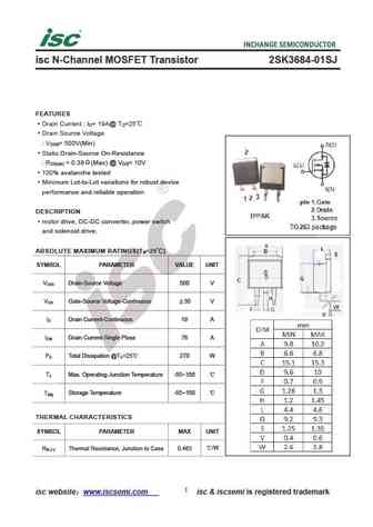
isc N-Channel MOSFET Transistor 2SK3684-01SJ FEATURES Drain Current I = 19A@ T =25 D C Drain Source Voltage V = 500V(Min) DSS Static Drain-Source On-Resistance R = 0.38 (Max) @ V = 10V DS(on) GS 100% avalanche tested Minimum Lot-to-Lot variations for robust device performance and reliable operation DESCRIPTION motor drive, DC-DC converter, power switch and s
2sk3698-01.pdf
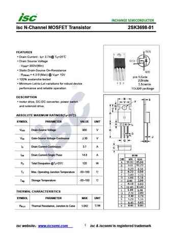
isc N-Channel MOSFET Transistor 2SK3698-01 FEATURES Drain Current I = 3.7A@ T =25 D C Drain Source Voltage V = 900V(Min) DSS Static Drain-Source On-Resistance R = 4.3 (Max) @ V = 10V DS(on) GS 100% avalanche tested Minimum Lot-to-Lot variations for robust device performance and reliable operation DESCRIPTION motor drive, DC-DC converter, power switch and sol
2sk3602-01.pdf

isc N-Channel MOSFET Transistor 2SK3602-01 FEATURES Drain Current I = 23A@ T =25 D C Drain Source Voltage V = 150V(Min) DSS Static Drain-Source On-Resistance R = 105m (Max) @ V = 10V DS(on) GS 100% avalanche tested Minimum Lot-to-Lot variations for robust device performance and reliable operation DESCRIPTION motor drive, DC-DC converter, power switch and sol
2sk3617i.pdf

isc N-Channel MOSFET Transistor 2SK3617I FEATURES Drain Current I = 6A@ T =25 D C Drain Source Voltage V = 100V(Min) DSS Static Drain-Source On-Resistance R = 225m (Max) @ V = 10V DS(on) GS 100% avalanche tested Minimum Lot-to-Lot variations for robust device performance and reliable operation DESCRIPTION motor drive, DC-DC converter, power switch and soleno
2sk3650-01l.pdf

isc N-Channel MOSFET Transistor 2SK3650-01L FEATURES Drain Current I = 33A@ T =25 D C Drain Source Voltage V = 150V(Min) DSS Static Drain-Source On-Resistance R = 70m (Max) @ V = 10V DS(on) GS 100% avalanche tested Minimum Lot-to-Lot variations for robust device performance and reliable operation DESCRIPTION motor drive, DC-DC converter, power switch and sol
2sk3676-01l.pdf
isc N-Channel MOSFET Transistor 2SK3676-01L FEATURES Drain Current I = 6.0A@ T =25 D C Drain Source Voltage V = 900V(Min) DSS Static Drain-Source On-Resistance R = 2.5 (Max) @ V = 10V DS(on) GS 100% avalanche tested Minimum Lot-to-Lot variations for robust device performance and reliable operation DESCRIPTION motor drive, DC-DC converter, power switch and so
Otros transistores... 2SK3506, 2SK3543, 2SK3561, 2SK3562, 2SK3563, 2SK3567, 2SK3568, 2SK3569, IRFB4110, 2SK3662, 2SK3667, 2SK3669, 2SK3797, 2SK3844, 2SK3846, 2SK3847, 2SK3869
Parámetros del MOSFET. Cómo se afectan entre sí.
🌐 : EN ES РУ

Liste
Recientemente añadidas las descripciónes de los transistores:
MOSFET: BC3134KT | BC3134K | BC2302W | BC2302T-2.8A | BC2302-2.8A | BC2301W | BC2301T-2.8A | CB3139KTB | CB2301DW | BC8205 | BC3415 | BC3407 | BC3401 | BC3400 | BC2301 | BC1012W
Popular searches
s9018 | 2n3904 equivalent | ksa1220 | s9015 | mje3055t datasheet | a733 | irf9630 | mj2955