RJK03E6DPA Datasheet. Equivalente. Reemplazo. Hoja de especificaciones. Principales características
Número de Parte: RJK03E6DPA
Tipo de FET: MOSFET
Polaridad de transistor: N
ESPECIFICACIONES MÁXIMAS
Pdⓘ - Máxima disipación de potencia: 35 W
|Vds|ⓘ - Voltaje máximo drenador-fuente: 30 V
|Vgs|ⓘ - Voltaje máximo fuente-puerta: 12 V
|Id|ⓘ - Corriente continua de drenaje: 35 A
Tjⓘ - Temperatura máxima de unión: 150 °C
CARACTERÍSTICAS ELÉCTRICAS
trⓘ - Tiempo de subida: 5.4 nS
Cossⓘ - Capacitancia de salida: 320 pF
RDSonⓘ - Resistencia estado encendido drenaje a fuente: 0.0046 Ohm
Encapsulados: WPAK
Búsqueda de reemplazo de RJK03E6DPA MOSFET
- Selecciónⓘ de transistores por parámetros
RJK03E6DPA datasheet
rej03g1930 rjk03e6dpads.pdf

Preliminary Datasheet RJK03E6DPA Silicon N Channel Power MOS FET with Schottky Barrier Diode REJ03G1930-0210 Power Switching Rev.2.10 May 20, 2010 Features High speed switching Capable of 4.5 V gate drive Low drive current High density mounting Low on-resistance RDS(on) = 3.8 m typ. (at VGS = 8 V) Pb-free Halogen-free Outline RENESA
rej03g1928 rjk03e4dpads.pdf
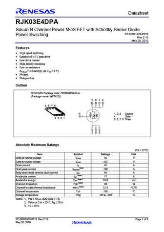
Preliminary Datasheet RJK03E4DPA Silicon N Channel Power MOS FET with Schottky Barrier Diode REJ03G1928-0210 Power Switching Rev.2.10 May 20, 2010 Features High speed switching Capable of 4.5 V gate drive Low drive current High density mounting Low on-resistance RDS(on) = 2.8 m typ. (at VGS = 8 V) Pb-free Halogen-free Outline RENESA
rej03g1933 rjk03e9dpads.pdf

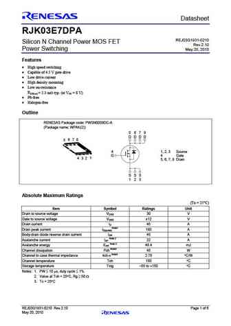
Preliminary Datasheet RJK03E9DPA REJ03G1933-0210 Silicon N Channel Power MOS FET Rev.2.10 Power Switching May 20, 2010 Features High speed switching Capable of 4.5 V gate drive Low drive current High density mounting Low on-resistance RDS(on) = 3.5 m typ. (at VGS = 8 V) Pb-free Halogen-free Outline RENESAS Package code PWSN0008DC-A
rej03g1932 rjk03e8dpads.pdf
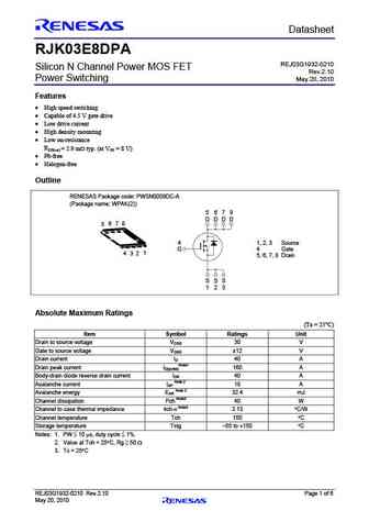
Preliminary Datasheet RJK03E8DPA REJ03G1932-0210 Silicon N Channel Power MOS FET Rev.2.10 Power Switching May 20, 2010 Features High speed switching Capable of 4.5 V gate drive Low drive current High density mounting Low on-resistance RDS(on) = 2.9 m typ. (at VGS = 8 V) Pb-free Halogen-free Outline RENESAS Package code PWSN0008DC-A
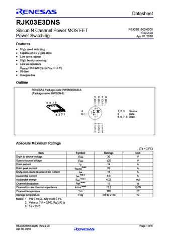


Otros transistores... RJK03C2DPB, RJK03C5DPA, RJK03E0DNS, RJK03E1DNS, RJK03E2DNS, RJK03E3DNS, RJK03E4DPA, RJK03E5DPA, 20N50, RJK03E7DPA, RJK03E8DPA, RJK03E9DPA, RJK03F0DPA, RJK03F6DNS, RJK03F7DNS, RJK03F8DNS, RJK03F9DNS
History: NCEP11N10AQU
🌐 : EN ES РУ

Liste
Recientemente añadidas las descripciónes de los transistores:
MOSFET: ASDM40N60KQ | ASDM40N40E | ASDM40N100P | ASDM40DN20E | ASDM3416EZA | ASDM3415ZA | ASDM3401ZA | ASDM3401 | ASDM3400ZA | ASDM30P30BE | RM50P30DF | CRTT095N12N | CRSS028N10N | CRST030N10N | CRJQ80N65F | ASDM20N20KQ
Popular searches
irf840 | irf740 | c945 transistor | irf640n | 2n3904 | bc547 datasheet | k3797 mosfet | bs170 datasheet