AO3407 Datasheet. Equivalente. Reemplazo. Hoja de especificaciones. Principales características
Número de Parte: AO3407 📄📄
Tipo de FET: MOSFET
Polaridad de transistor: P
ESPECIFICACIONES MÁXIMAS
Pdⓘ - Máxima disipación de potencia: 1.4 W
|Vds|ⓘ - Voltaje máximo drenador-fuente: 30 V
|Vgs|ⓘ - Voltaje máximo fuente-puerta: 20 V
|Id|ⓘ - Corriente continua de drenaje: 5.3 A
Tjⓘ - Temperatura máxima de unión: 150 °C
CARACTERÍSTICAS ELÉCTRICAS
trⓘ - Tiempo de subida: 2.33 nS
Cossⓘ - Capacitancia de salida: 90 pF
RDSonⓘ - Resistencia estado encendido drenaje a fuente: 0.0645 Ohm
Encapsulados: SOT23
📄📄 Copiar
Búsqueda de reemplazo de AO3407 MOSFET
- Selecciónⓘ de transistores por parámetros
AO3407 datasheet
..1. Size:2288K 1
ao3407 a7 a79t x7kv code psot23.pdf 
SMD Type MOSFET P-Channel MOSFET AO3407A (KO3407A) SOT-23-3 Unit mm +0.2 2.9 -0.1 +0.1 0.4 -0.1 3 Features VDS (V) =-30V ID =-4.3 A (VGS =-10V) 1 2 RDS(ON) 48m (VGS =-10V) +0.02 +0.1 0.15 -0.02 0.95-0.1 +0.1 1.9-0.2 RDS(ON) 78m (VGS =-4.5V) 1. Gate 2. Source 3. Drain D D G G S S Absolute Maximum Ratings Ta = 25 Paramete
..2. Size:1986K htsemi
ao3407.pdf
AO3407 30V P-Channel Enhancement Mode MOSFET V = -30V DS R , V DS(ON) gs@-10V, I 4.1A
..3. Size:447K aosemi
ao3407.pdf
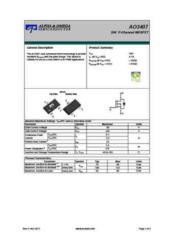
AO3407 30V P-Channel MOSFET General Description Product Summary VDS -30V The AO3407 uses advanced trench technology to provide excellent RDS(ON) with low gate charge. This device is ID (at VGS=10V) -4.1A suitable for use as a load switch or in PWM applications. RDS(ON) (at VGS=10V)
..4. Size:1220K shenzhen
ao3407.pdf
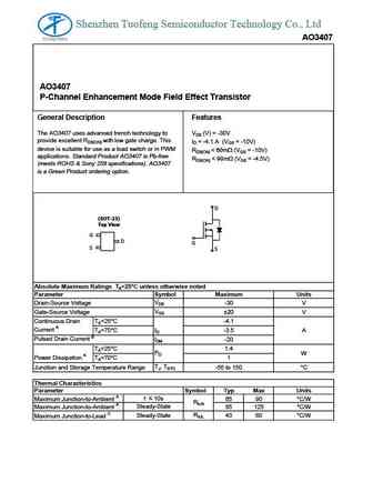
Shenzhen Tuofeng Semiconductor Technology Co., Ltd AO3407 AO3407 P-Channel Enhancement Mode Field Effect Transistor General Description Features The AO3407 uses advanced trench technology to VDS (V) = -30V provide excellent RDS(ON) with low gate charge. This ID = -4.1 A (VGS = -10V) device is suitable for use as a load switch or in PWM RDS(ON)
..5. Size:1542K kexin
ao3407.pdf
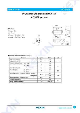
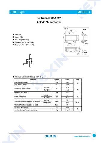
SMD Type IC SMD Type MOSFET P-Channel Enhancement MOSFET AO3407 (KO3407) SOT-23 Unit mm +0.1 2.9 -0.1 +0.1 0.4 -0.1 Features 3 VDS (V) = -30V ID = -4.1 A 1 2 RDS(ON) 52m (VGS = -10V) D +0.1 +0.05 0.95 -0.1 0.1 -0.01 +0.1 RDS(ON) 87m (VGS = -4.5V) 1.9 -0.1 1.Base 1. Gate 2.Emitter 2. Source G 3. Drain 3.collector S Absolute Maximum Ratings Ta = 25 Parameter Sy
..6. Size:1572K kexin
ao3407 ko3407.pdf

SMD Type IC SMD Type MOSFET P-Channel Enhancement MOSFET AO3407 (KO3407) SOT-23-3 Unit mm +0.2 2.9-0.1 +0.1 0.4 -0.1 3 Features VDS (V) = -30V ID = -4.1 A 1 2 +0.02 +0.1 0.15 -0.02 RDS(ON) 52m (VGS = -10V) 0.95 -0.1 D 1.9+0.1 -0.2 RDS(ON) 87m (VGS = -4.5V) 1. Gate 2. Source G 3. Drain S Absolute Maximum Ratings Ta = 25 Parameter Symbol Rating Unit Drain-Sourc
..7. Size:493K guangdong hottech
ao3407.pdf
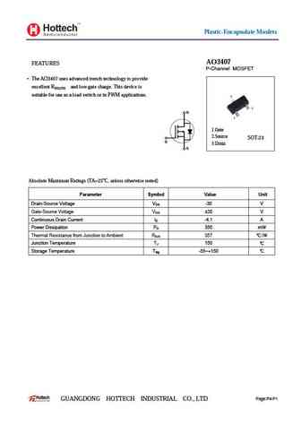
Plastic-Encapsulate Mosfets AO3407 FEATURES P-Channel MOSFET The AO3407 uses advanced trench technology to provide excellent RDS(ON) and low gate charge. This device is suitable for use as a load switch or in PWM applications. D D 1.Gate 2.Source SOT-23 G G 3.Drain S S Absolute Maximum Ratings (TA=25oC, unless otherwise noted) Parameter Symbol Value Unit Drain-Source Voltage
..8. Size:1487K mdd
ao3407.pdf
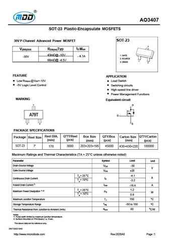
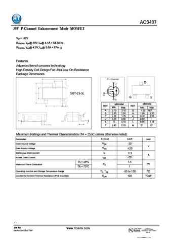
AO3407 SOT-23 Plastic-Encapsulate MOSFETS SOT-23 30V P-Channel Advanced Power MOSFET 3 ID Max V(BR)DSS RDS(on)Typ 43m @ -10V 1. GATE - 4.1A -30V 2. SOURCE 66m @ -4.5V 1 3. DRAIN 2 FEATURE APPLICATION Low RDS(on) @VGS=-10V Load Switch -5V Logic Level Control Switching circuits High-speed line driver Power Management Functions M
..9. Size:500K cn puolop
ao3407.pdf
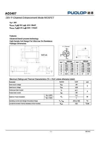
AO3407 -30V P-Channel Enhancement Mode MOSFET V = -30V DS R , V DS(ON) gs@-10V, I -4.1A
..10. Size:782K cn shikues
ao3407.pdf
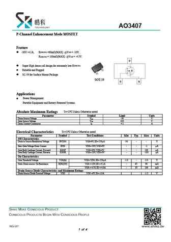
AO3407 P-Channel Enhancement Mode MOSFET Feature DS(ON) GS -30V/-4.1A, R =80m (MAX) @V = -10V. DS(ON) GS R = 100m (MAX) @V = -4.5V. . DS(ON) Super High dense cell design for extremely low R Reliable and Rugged SC-59 for Surface Mount Package SOT-59 Applications Power Management Portable Equipment and Battery Powered Systems. A T =25 Unless Ot
..11. Size:999K cn alj
ao3407.pdf
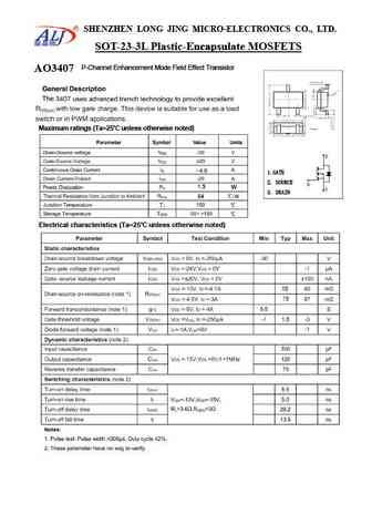
SHENZHEN LONG JING MICRO-ELECTRONICS CO., LTD. SOT-23-3L Plastic-Encapsulate MOSFETS Encapsu P-Channel Enhancement Mode Field Effect Transistor A O34 0 7 Maximum ratings (Ta=25 unless otherwise noted) 4.6 1.GATE 2. SOURCE 1.5 W 3. DRAIN 84 Electrical characteristics (Ta=25 unless otherwise noted) 55 75 1.5
..12. Size:2101K cn twgmc
ao3407.pdf
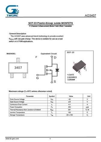
AO3407 SI2305 AO3401 SI2301 SOT-23 Plastic-Encap sulate MOSFETS P-Channel Enhancement Mode Field Effect Transistor P-Channel Enhancement Mode Field Effect Transistor P-Channel Enhancement Mode Field Effect Transistor P-Channel Enhancement Mode Field Effect Transistor P-Channel Enhancement Mode Field Effect Transistor SI2301 General Description The BC3407 uses advanced trench techno
..13. Size:866K cn vbsemi
ao3407.pdf
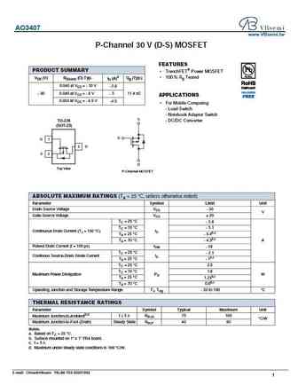
AO3407 www.VBsemi.tw P-Channel 30 V (D-S) MOSFET FEATURES PRODUCT SUMMARY TrenchFET Power MOSFET 100 % Rg Tested VDS (V) RDS(on) ( ) Typ. ID (A)a Qg (Typ.) 0.046 at VGS = - 10 V - 5.6 0.049 at VGS = - 6 V - 5 11.4 nC - 30 APPLICATIONS 0.054 at VGS = - 4.5 V -4.5 For Mobile Computing - Load Switch - Notebook Adaptor Switch S TO-236 - DC/DC Converter (SOT-23)
0.1. Size:484K aosemi
ao3407a.pdf
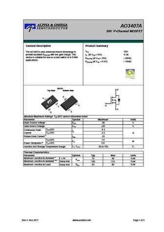
AO3407A 30V P-Channel MOSFET General Description Product Summary VDS -30V The AO3407A uses advanced trench technology to provide excellent RDS(ON) with low gate charge. This ID (at VGS=-10V) -4.3A device is suitable for use as a load switch or in PWM RDS(ON) (at VGS=-10V)
0.2. Size:2288K kexin
ao3407a-3.pdf

SMD Type MOSFET P-Channel MOSFET AO3407A (KO3407A) SOT-23-3 Unit mm +0.2 2.9 -0.1 +0.1 0.4 -0.1 3 Features VDS (V) =-30V ID =-4.3 A (VGS =-10V) 1 2 RDS(ON) 48m (VGS =-10V) +0.02 +0.1 0.15 -0.02 0.95-0.1 +0.1 1.9-0.2 RDS(ON) 78m (VGS =-4.5V) 1. Gate 2. Source 3. Drain D D G G S S Absolute Maximum Ratings Ta = 25 Paramete
0.3. Size:2287K kexin
ao3407a.pdf
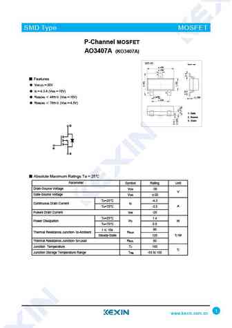
SMD Type MOSFET P-Channel MOSFET AO3407A (KO3407A) SOT-23 Unit mm 2.9+0.1 -0.1 +0.1 0.4-0.1 3 Features VDS (V) =-30V ID =-4.3 A (VGS =-10V) 1 2 +0.1 +0.05 0.95 -0.1 RDS(ON) 48m (VGS =-10V) 0.1 -0.01 +0.1 1.9 -0.1 RDS(ON) 78m (VGS =-4.5V) 1. Gate 2. Source 3. Drain D D G G S S Absolute Maximum Ratings Ta = 25 Parameter Sy
0.4. Size:1559K kexin
ao3407hf.pdf
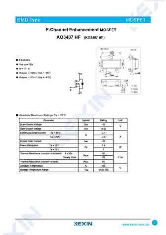
SMD Type IC SMD Type MOSFET P-Channel Enhancement MOSFET AO3407 HF (KO3407 HF) SOT-23-3 Unit mm +0.2 2.9-0.1 +0.1 0.4 -0.1 3 Features VDS (V) = -30V ID = -4.1 A 1 2 +0.02 +0.1 0.15 -0.02 RDS(ON) 52m (VGS = -10V) 0.95 -0.1 D 1.9+0.1 -0.2 RDS(ON) 87m (VGS = -4.5V) 1. Gate 2. Source G 3. Drain S Absolute Maximum Ratings Ta = 25 Parameter Symbol Rating Unit Drain-
0.5. Size:1572K kexin
ao3407-3.pdf
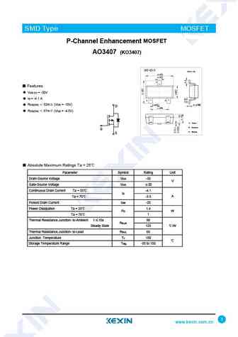
SMD Type IC SMD Type MOSFET P-Channel Enhancement MOSFET AO3407 (KO3407) SOT-23-3 Unit mm +0.2 2.9-0.1 +0.1 0.4 -0.1 3 Features VDS (V) = -30V ID = -4.1 A 1 2 +0.02 +0.1 0.15 -0.02 RDS(ON) 52m (VGS = -10V) 0.95 -0.1 D 1.9+0.1 -0.2 RDS(ON) 87m (VGS = -4.5V) 1. Gate 2. Source G 3. Drain S Absolute Maximum Ratings Ta = 25 Parameter Symbol Rating Unit Drain-Sourc
0.6. Size:276K lzg
ao3407g.pdf
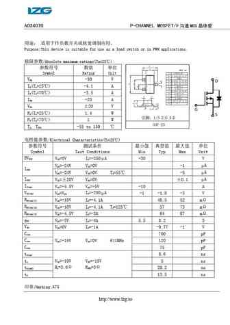
AO3407G P-CHANNEL MOSFET/P MOS Purpose This device is suitable for use as a load switch or in PWM applications. /Absolute maximum ratings(Ta=25 ) Symbol Rating Unit V -30 V DS I (T =25 ) -4.1 A D a I (T =70 ) -3.5 A D a I -20 A DM V 20 V GS P (
0.7. Size:2084K umw-ic
ao3407a.pdf
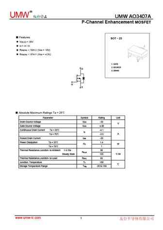
R UMW UMW AO3407A UMW AO3407A UMW AO3407A P-Channel Enhancement MOSFET Features SOT 23 VDS (V) = -30V ID = -4.1 A RDS(ON) 52m (VGS = -10V) RDS(ON) 87m (VGS = -4.5V) 1. GATE 2. SOURCE D 3. DRAIN G S Absolute Maximum Ratings Ta = 25 Parameter Symbol Rating Unit Drain-Source Voltage VDS -30 V Gate-Source Voltage VGS 20 Continuous Drain Current Ta = 25 -4.1
0.8. Size:476K huashuo
ao3407a.pdf
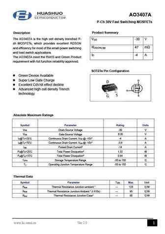
AO3407A P-Ch 30V Fast Switching MOSFETs Product Summary Description The AO3407A is the high cell density trenched P- V -30 V DS ch MOSFETs, which provides excellent RDSON R 47 m DS(ON),typ and efficiency for most of the small power switching and load switch applications. I -4 A D The AO3407A meet the RoHS and Green Product requirement with full function reliability a
Otros transistores... PT8205A, PT8822, PT4410, PT9926, SI2301, SI2305, XP152A12COMR, AO3401, STF13NM60N, PT4435, SM103, SM104, SMY50, SMY51, SMY52, SMY60, U105D