CEP07N7 MOSFET Equivalente. Reemplazo. Hoja de especificaciones. Principales características
Número de Parte: CEP07N7
Tipo de FET: MOSFET
Polaridad de transistor: N
ESPECIFICACIONES MÁXIMAS
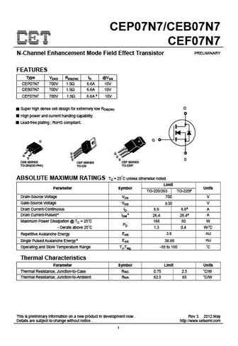
Pdⓘ - Máxima
disipación de potencia: 166 W
|Vds|ⓘ - Voltaje máximo drenador-fuente: 700 V
|Vgs|ⓘ - Voltaje máximo fuente-puerta: 30 V
|Id|ⓘ - Corriente continua
de drenaje: 6.6 A
Tjⓘ - Temperatura máxima de unión: 150 °C
CARACTERÍSTICAS ELÉCTRICAS
trⓘ - Tiempo
de subida: 19 nS
Cossⓘ - Capacitancia de salida: 125 pF
RDSonⓘ - Resistencia estado encendido drenaje a fuente: 1.5 Ohm
Encapsulados: TO220
Búsqueda de reemplazo de CEP07N7 MOSFET
- Selecciónⓘ de transistores por parámetros
CEP07N7 datasheet
..1. Size:434K cet
cep07n7 ceb07n7 cef07n7.pdf 

CEP07N7/CEB07N7 CEF07N7 PRELIMINARY N-Channel Enhancement Mode Field Effect Transistor FEATURES Type VDSS RDS(ON) ID @VGS CEP07N7 700V 1.5 6.6A 10V CEB07N7 700V 1.5 6.6A 10V CEF07N7 700V 1.5 6.6A d 10V D Super high dense cell design for extremely low RDS(ON). High power and current handing capability. Lead-free plating ; RoHS compliant. G S CEB SERIES CEP SERIES CEF SER
8.1. Size:432K cet
cep07n65 ceb07n65 cef07n65.pdf 

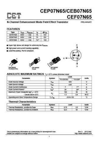
CEP07N65/CEB07N65 CEF07N65 PRELIMINARY N-Channel Enhancement Mode Field Effect Transistor FEATURES Type VDSS RDS(ON) ID @VGS CEP07N65 650V 1.3 7A 10V CEB07N65 650V 1.3 7A 10V CEF07N65 650V 1.3 7A d 10V D Super high dense cell design for extremely low RDS(ON). High power and current handing capability. Lead-free plating ; RoHS compliant. G S CEB SERIES CEP SERIES CEF SER
8.2. Size:375K cet
cep07n65a ceb07n65a cef07n65a.pdf 

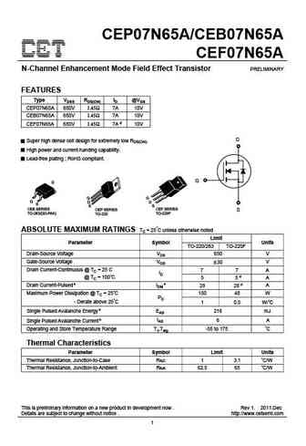
CEP07N65A/CEB07N65A CEF07N65A N-Channel Enhancement Mode Field Effect Transistor PRELIMINARY FEATURES Type VDSS RDS(ON) ID @VGS CEP07N65A 650V 1.45 7A 10V CEB07N65A 650V 1.45 7A 10V CEF07N65A 650V 1.45 7A d 10V D Super high dense cell design for extremely low RDS(ON). High power and current handing capability. Lead-free plating ; RoHS compliant. G CEB SERIES CEP SERIES CE
9.1. Size:331K ncepower
ncep075n85agu.pdf 

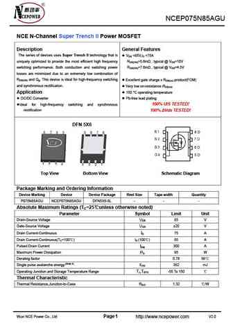
NCEP075N85AGU NCE N-Channel Super Trench II Power MOSFET Description General Features The series of devices uses Super Trench II technology that is VDS =85V,ID =75A uniquely optimized to provide the most efficient high frequency RDS(ON)=5.6m , typical @ VGS=10V switching performance. Both conduction and switching power RDS(ON)=7.6m , typical @ VGS=4.5V losses are minimiz
9.2. Size:760K ncepower
ncep075n85gu.pdf 

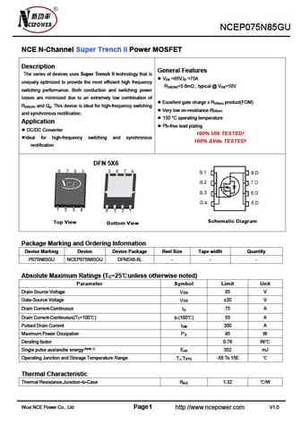
NCEP075N85GU NCE N-Channel Super Trench II Power MOSFET Description General Features The series of devices uses Super Trench II technology that is V =85V,I =75A DS D uniquely optimized to provide the most efficient high frequency R =5.6m , typical @ V =10V DS(ON) GS switching performance. Both conduction and switching power losses are minimized due to an extremely low combinati
9.3. Size:305K ncepower
ncep072n10.pdf 

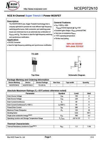
http //www.ncepower.com NCEP072N10 NCE N-Channel Super Trench II Power MOSFET Description General Features The NCEP072N10 uses Super Trench II technology that is VDS =100V,ID =90A uniquely optimized to provide the most efficient high frequency RDS(ON)=6.8m (typical) @ VGS=10V switching performance. Both conduction and switching power Excellent gate charge x RDS(on) p
9.4. Size:397K ncepower
ncep070n10agu.pdf 

NCEP070N10AGU NCE N-Channel Super Trench II Power MOSFET Description General Features The series of devices uses Super Trench II technology that is VDS =100V,ID =80A uniquely optimized to provide the most efficient high frequency RDS(ON)=6.1m , typical@ VGS=10V switching performance. Both conduction and switching power RDS(ON)=8.35m , typical@ VGS=4.5V losses are minimiz
9.5. Size:335K ncepower
ncep070n12.pdf 

NCEP070N12,NCEP070N12D NCE N-Channel Super Trench II Power MOSFET Description General Features The series of devices uses Super Trench II technology that is VDS =120V,ID =100A uniquely optimized to provide the most efficient high frequency RDS(ON)=6.5m , typical (TO-220)@ VGS=10V switching performance. Both conduction and switching power RDS(ON)=6.3m , typical (TO-26
9.6. Size:335K ncepower
ncep070n12 ncep070n12d.pdf 

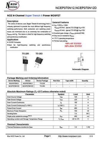
NCEP070N12,NCEP070N12D NCE N-Channel Super Trench II Power MOSFET Description General Features The series of devices uses Super Trench II technology that is VDS =120V,ID =100A uniquely optimized to provide the most efficient high frequency RDS(ON)=6.5m , typical (TO-220)@ VGS=10V switching performance. Both conduction and switching power RDS(ON)=6.3m , typical (TO-26
9.7. Size:335K ncepower
ncep070n12d.pdf 

NCEP070N12,NCEP070N12D NCE N-Channel Super Trench II Power MOSFET Description General Features The series of devices uses Super Trench II technology that is VDS =120V,ID =100A uniquely optimized to provide the most efficient high frequency RDS(ON)=6.5m , typical (TO-220)@ VGS=10V switching performance. Both conduction and switching power RDS(ON)=6.3m , typical (TO-26
9.8. Size:462K ncepower
ncep078n10ak.pdf 

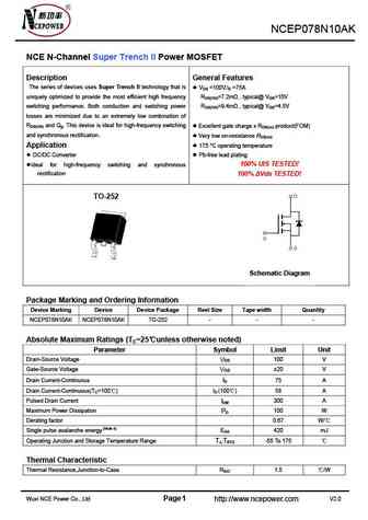
NCEP078N10AK NCE N-Channel Super Trench II Power MOSFET Description General Features The series of devices uses Super Trench II technology that is VDS =100V,ID =75A uniquely optimized to provide the most efficient high frequency RDS(ON)=7.2m , typical@ VGS=10V switching performance. Both conduction and switching power RDS(ON)=9.4m , typical@ VGS=4.5V losses are minimized
9.9. Size:627K ncepower
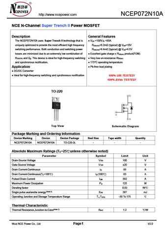
ncep072n10a.pdf 

http //www.ncepower.com NCEP072N10A NCE N-Channel Super Trench II Power MOSFET Description General Features The NCEP072N10A uses Super Trench II technology that is V =100V,I =88A DS D uniquely optimized to provide the most efficient high frequency R =6.2m (typical) @ V =10V DS(ON) GS switching performance. Both conduction and switching power R =8.4m (typical) @ V =4.5V DS(ON) GS
9.10. Size:377K ncepower
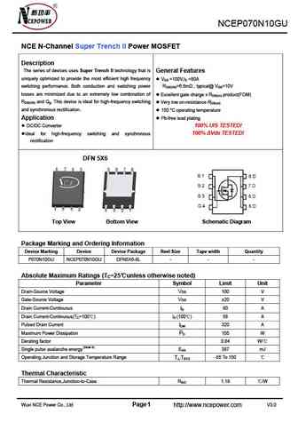
ncep070n10gu.pdf 

NCEP070N10GU NCE N-Channel Super Trench II Power MOSFET Description The series of devices uses Super Trench II technology that is General Features uniquely optimized to provide the most efficient high frequency VDS =100V,ID =80A switching performance. Both conduction and switching power RDS(ON)=6.6m , typical@ VGS=10V losses are minimized due to an extremely low combinati
9.11. Size:428K ncepower
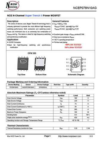
ncep078n10ag.pdf 

NCEP078N10AG NCE N-Channel Super Trench II Power MOSFET Description General Features The series of devices uses Super Trench II technology that is VDS =100V,ID =75A uniquely optimized to provide the most efficient high frequency RDS(ON)=7.0m , typical@ VGS=10V switching performance. Both conduction and switching power RDS(ON)=9.2m , typical@ VGS=4.5V losses are minimized
9.12. Size:1009K ncepower
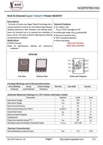
ncep078n10g.pdf 

NCEP078N10G NCE N-Channel Super Trench II Power MOSFET Description The series of devices uses Super Trench II technology that is General Features uniquely optimized to provide the most efficient high frequency V =100V,I =75A DS D switching performance. Both conduction and switching power R =7.4m , typical@ V =10V DS(ON) GS losses are minimized due to an extremely low combination
Otros transistores... CEP03N8, CEP04N6, CEP04N65, CEP04N7G, CEP05N65, CEP06N7, CEP07N65, CEP07N65A, IRF1010E, CEB13N5A, CEF13N5A, CEP13N5A, CEB08N8, CEF08N8, CEP08N8, CEB20A03, CEP20A03
