FDG311N MOSFET Equivalente. Reemplazo. Hoja de especificaciones. Principales características
Número de Parte: FDG311N
Tipo de FET: MOSFET
Polaridad de transistor: N
ESPECIFICACIONES MÁXIMAS
Pdⓘ - Máxima disipación de potencia: 0.75 W
|Vds|ⓘ - Voltaje máximo drenador-fuente: 20 V
|Vgs|ⓘ - Voltaje máximo fuente-puerta: 8 V
|Id|ⓘ - Corriente continua de drenaje: 1.9 A
Tjⓘ - Temperatura máxima de unión: 150 °C
CARACTERÍSTICAS ELÉCTRICAS
trⓘ - Tiempo de subida: 9 nS
Cossⓘ - Capacitancia de salida: 55 pF
RDSonⓘ - Resistencia estado encendido drenaje a fuente: 0.115 Ohm
Encapsulados: SC70-6
Búsqueda de reemplazo de FDG311N MOSFET
- Selecciónⓘ de transistores por parámetros
FDG311N datasheet
fdg311n.pdf
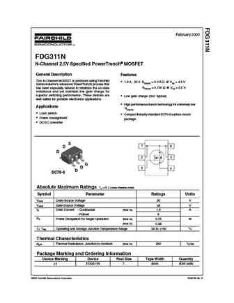
February 2000 FDG311N N-Channel 2.5V Specified PowerTrench MOSFET General Description Features This N-Channel MOSFET is produced using Fairchild 1.9 A, 20 V. RDS(ON) = 0.115 @ VGS = 4.5 V Semiconductor's advanced PowerTrench process that RDS(ON) = 0.150 @ VGS = 2.5 V. has been especially tailored to minimize the on-state resistance and yet maintain lo
fdg311n.pdf

Is Now Part of To learn more about ON Semiconductor, please visit our website at www.onsemi.com Please note As part of the Fairchild Semiconductor integration, some of the Fairchild orderable part numbers will need to change in order to meet ON Semiconductor s system requirements. Since the ON Semiconductor product management systems do not have the ability to manage part nomenclatur
fdg313n d87z.pdf

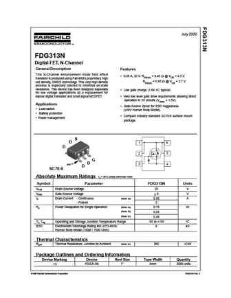
July 2000 FDG313N Digital FET, N-Channel General Description Features This N-Channel enhancement mode field effect 0.95 A, 25 V. RDS(on) = 0.45 @ VGS = 4.5 V transistor is produced using Fairchild's proprietary, high RDS(on) = 0.60 @ VGS = 2.7 V. cell density, DMOS technology. This very high density process is especially tailored to minimize on-state resistance. This devic
fdg315n.pdf
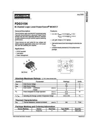
July 2000 FDG315N N-Channel Logic Level PowerTrench MOSFET General Description Features This N-Channel Logic Level MOSFET is produced using 2 A, 30 V. RDS(ON) = 0.12 @ VGS = 10 V Fairchild Semiconductor's advanced PowerTrench RDS(ON) = 0.16 @ VGS = 4.5 V. process that has been especially tailored to minimize on-state resistance and yet maintain super

Otros transistores... FDD5690, FDD6030L, FDD6612A, FDD6670A, FDD6680, FDD6680A, FDD6690A, AS3402, 8N60, FDG312P, FDG313N, FDG314P, FDG315N, FDG316P, FDG6301N, FDG6302P, FDG6303N
🌐 : EN ES РУ

Liste
Recientemente añadidas las descripciónes de los transistores:
MOSFET: AUP060N055 | AUP056N10 | AUP056N08BGL | AUP052N085 | AUP045N12 | AUP039N10 | AUP034N10 | AUP034N06 | AUP033N08BG | AUP026N085 | AUN084N10 | AUN065N10 | AUN063N10 | AUN062N08BG | AUN060N08AG | AUN053N10
Popular searches
2sc828 replacement | 2sd669 datasheet | c102 transistor | bt152 datasheet | 2sa1302 datasheet | mpsa13 transistor equivalent | кт817г характеристики | 2sc1972