CEP05P03 MOSFET Equivalente. Reemplazo. Hoja de especificaciones. Principales características
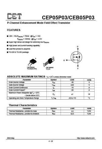
Número de Parte: CEP05P03
Tipo de FET: MOSFET
Polaridad de transistor: P
ESPECIFICACIONES MÁXIMAS
Pdⓘ - Máxima
disipación de potencia: 47 W
|Vds|ⓘ - Voltaje máximo drenador-fuente: 30 V
|Vgs|ⓘ - Voltaje máximo fuente-puerta: 20 V
|Id|ⓘ - Corriente continua
de drenaje: 18 A
Tjⓘ - Temperatura máxima de unión: 175 °C
CARACTERÍSTICAS ELÉCTRICAS
trⓘ - Tiempo
de subida: 11 nS
Cossⓘ - Capacitancia de salida: 420 pF
RDSonⓘ - Resistencia estado encendido drenaje a fuente: 0.07 Ohm
Encapsulados: TO220
Búsqueda de reemplazo de CEP05P03 MOSFET
- Selecciónⓘ de transistores por parámetros
CEP05P03 datasheet
..1. Size:176K cet
cep05p03 ceb05p03.pdf 

CEP05P03/CEB05P03 P-Channel Enhancement Mode Field Effect Transistor FEATURES -30V, -18A,RDS(ON) = 70m @VGS = -10V. RDS(ON) = 120m @VGS = -4.5V. Super high dense cell design for extremely low RDS(ON). High power and current handing capability. D Lead free product is acquired. TO-220 & TO-263 package. G CEB SERIES CEP SERIES S TO-263(DD-PAK) TO-220 ABSOLUTE MAXIMUM RATINGS
9.1. Size:427K cet
cep05n65 ceb05n65 cef05n65.pdf 

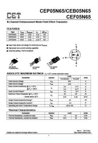
CEP05N65/CEB05N65 CEF05N65 N-Channel Enhancement Mode Field Effect Transistor FEATURES Type VDSS RDS(ON) ID @VGS CEP05N65 650V 2.4 4.5A 10V CEB05N65 650V 2.4 4.5A 10V CEF05N65 650V 2.4 4.5A d 10V D Super high dense cell design for extremely low RDS(ON). High power and current handing capability. Lead-free plating ; RoHS compliant. G S CEB SERIES CEP SERIES CEF SERIES TO
9.2. Size:344K cet
ceb05n8 cef05n8 cep05n8.pdf 

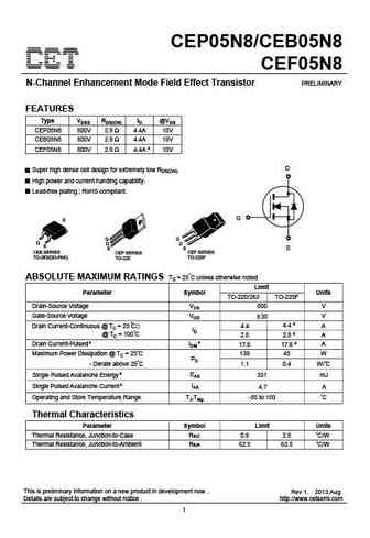
CEP05N8/CEB05N8 CEF05N8 N-Channel Enhancement Mode Field Effect Transistor PRELIMINARY FEATURES Type VDSS RDS(ON) ID @VGS CEP05N8 800V 2.9 4.4A 10V CEB05N8 800V 2.9 4.4A 10V CEF05N8 800V 2.9 4.4A d 10V D Super high dense cell design for extremely low RDS(ON). High power and current handing capability. Lead-free plating ; RoHS compliant. G S CEB SERIES CEP SERIES CEF S
9.3. Size:1315K ncepower
ncep050n12d.pdf 

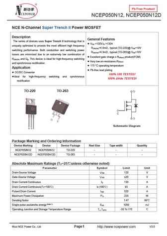
Pb Free Product NCEP050N12, NCEP050N12D NCE N-Channel Super Trench II Power MOSFET Description General Features The series of devices uses Super Trench II technology that is V =120V,I =130A DS D uniquely optimized to provide the most efficient high frequency R =4.5m , typical (TO-220)@ V =10V DS(ON) GS switching performance. Both conduction and switching power R =4.3m , typi
9.4. Size:311K ncepower
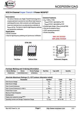
ncep055n12ag.pdf 

NCEP055N12AG NCE N-Channel Super Trench II Power MOSFET Description General Features The series of devices uses Super Trench II technology that is VDS =120V,ID =110A uniquely optimized to provide the most efficient high frequency RDS(ON)=5.2m , typical @ VGS=10V switching performance. Both conduction and switching power RDS(ON)=6.4m , typical @ VGS=4.5V losses are m
9.5. Size:1315K ncepower
ncep050n12.pdf 

Pb Free Product NCEP050N12, NCEP050N12D NCE N-Channel Super Trench II Power MOSFET Description General Features The series of devices uses Super Trench II technology that is V =120V,I =130A DS D uniquely optimized to provide the most efficient high frequency R =4.5m , typical (TO-220)@ V =10V DS(ON) GS switching performance. Both conduction and switching power R =4.3m , typi
9.6. Size:396K ncepower
ncep050n85 ncep050n85d.pdf 

NCEP050N85, NCEP050N85D NCE N-Channel Super Trench II Power MOSFET Description The series of devices uses Super Trench II technology that is General Features uniquely optimized to provide the most efficient high frequency VDS =85V,ID =120A switching performance. Both conduction and switching power RDS(ON)=4.7m , typical (TO-220)@ VGS=10V losses are minimized due to an ext
9.7. Size:329K ncepower
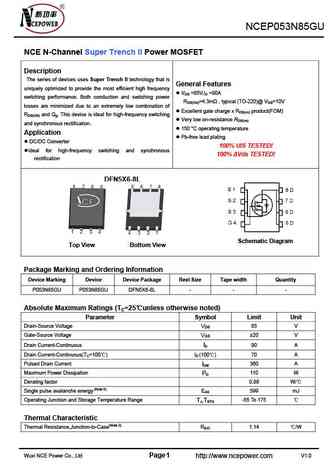
ncep053n85gu.pdf 

NCEP053N85GU NCE N-Channel Super Trench II Power MOSFET Description The series of devices uses Super Trench II technology that is General Features uniquely optimized to provide the most efficient high frequency VDS =85V,ID =90A switching performance. Both conduction and switching power RDS(ON)=4.3m , typical (TO-220)@ VGS=10V losses are minimized due to an extremely low
9.8. Size:342K ncepower
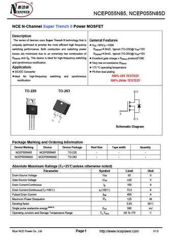
ncep055n85.pdf 

NCEP055N85, NCEP055N85D NCE N-Channel Super Trench II Power MOSFET Description The series of devices uses Super Trench II technology that is General Features uniquely optimized to provide the most efficient high frequency VDS =85V,ID =100A switching performance. Both conduction and switching power RDS(ON)=4.8m , typical (TO-220)@ VGS=10V losses are minimized due to an ext
9.9. Size:342K ncepower
ncep055n85 ncep055n85d.pdf 

NCEP055N85, NCEP055N85D NCE N-Channel Super Trench II Power MOSFET Description The series of devices uses Super Trench II technology that is General Features uniquely optimized to provide the most efficient high frequency VDS =85V,ID =100A switching performance. Both conduction and switching power RDS(ON)=4.8m , typical (TO-220)@ VGS=10V losses are minimized due to an ext
9.10. Size:345K ncepower
ncep058n85.pdf 

NCEP058N85, NCEP058N85D NCE N-Channel Super Trench II Power MOSFET Description The series of devices uses Super Trench II technology that is General Features uniquely optimized to provide the most efficient high frequency VDS =85V,ID =95A switching performance. Both conduction and switching power RDS(ON)=5.4m , typical (TO-220)@ VGS=10V losses are minimized due to an extr
9.11. Size:420K ncepower
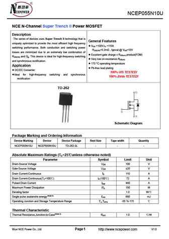
ncep055n10u.pdf 

NCEP055N10U NCE N-Channel Super Trench II Power MOSFET Description The series of devices uses Super Trench II technology that is General Features uniquely optimized to provide the most efficient high frequency VDS =100V,ID =110A switching performance. Both conduction and switching power RDS(ON)=5.2m , typical @ VGS=10V losses are minimized due to an extremely low combin
9.12. Size:395K ncepower
ncep050n85.pdf 

NCEP050N85, NCEP050N85D NCE N-Channel Super Trench II Power MOSFET Description The series of devices uses Super Trench II technology that is General Features uniquely optimized to provide the most efficient high frequency VDS =85V,ID =115A switching performance. Both conduction and switching power RDS(ON)=4.7m , typical (TO-220)@ VGS=10V losses are minimized due to an ext
9.13. Size:323K ncepower
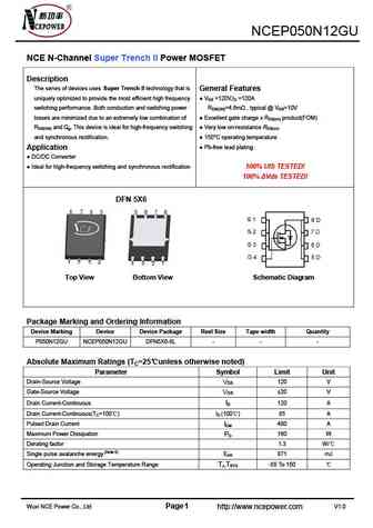
ncep050n12gu.pdf 

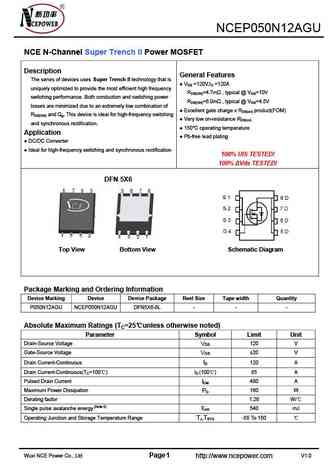
NCEP050N12GU NCE N-Channel Super Trench II Power MOSFET Description The series of devices uses Super Trench II technology that is General Features uniquely optimized to provide the most efficient high frequency VDS =120V,ID =120A switching performance. Both conduction and switching power RDS(ON)=4.6m , typical @ VGS=10V losses are minimized due to an extremely low combinatio
9.14. Size:736K ncepower
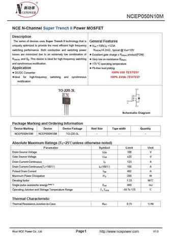
ncep050n10m.pdf 

NCEP050N10M NCE N-Channel Super Trench II Power MOSFET Description The series of devices uses Super Trench II technology that is General Features uniquely optimized to provide the most efficient high frequency V =100V,I =123A DS D switching performance. Both conduction and switching power R =4.2m , typical @ V =10V DS(ON) GS losses are minimized due to an extremely low combinati
9.15. Size:395K ncepower
ncep050n85d.pdf 

NCEP050N85, NCEP050N85D NCE N-Channel Super Trench II Power MOSFET Description The series of devices uses Super Trench II technology that is General Features uniquely optimized to provide the most efficient high frequency VDS =85V,ID =115A switching performance. Both conduction and switching power RDS(ON)=4.7m , typical (TO-220)@ VGS=10V losses are minimized due to an ext
9.16. Size:405K ncepower
ncep055n10.pdf 

NCEP055N10, NCEP055N10D NCE N-Channel Super Trench II Power MOSFET Description The series of devices uses Super Trench II technology that is General Features uniquely optimized to provide the most efficient high frequency VDS =100V,ID =110A switching performance. Both conduction and switching power RDS(ON)=5.4m , typical (TO-220)@ VGS=10V losses are minimized due to an ex
9.17. Size:342K ncepower
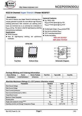
ncep055n30gu.pdf 

http //www.ncepower.com NCEP055N30GU NCE N-Channel Super Trench II Power MOSFET Description General Features The series of devices uses Super Trench II technology that is VDS =30V,ID =55A uniquely optimized to provide the most efficient high frequency RDS(ON)=4.2m (typical) @ VGS=10V switching performance. Both conduction and switching power RDS(ON)=7.4m (typical) @
9.18. Size:328K ncepower
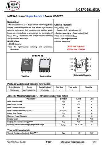
ncep058n85gu.pdf 

NCEP058N85GU NCE N-Channel Super Trench II Power MOSFET Description The series of devices uses Super Trench II technology that is General Features uniquely optimized to provide the most efficient high frequency VDS =85V,ID =90A switching performance. Both conduction and switching power RDS(ON)=4.8m , typical@ VGS=10V losses are minimized due to an extremely low combinatio
9.19. Size:345K ncepower
ncep058n85d.pdf 

NCEP058N85, NCEP058N85D NCE N-Channel Super Trench II Power MOSFET Description The series of devices uses Super Trench II technology that is General Features uniquely optimized to provide the most efficient high frequency VDS =85V,ID =95A switching performance. Both conduction and switching power RDS(ON)=5.4m , typical (TO-220)@ VGS=10V losses are minimized due to an extr
9.20. Size:363K ncepower
ncep055n60gu.pdf 

http //www.ncepower.com NCEP055N60GU NCE N-Channel Super Trench II Power MOSFET Description General Features The NCEP055N60GU uses Super Trench II technology that is VDS =60V,ID =75A uniquely optimized to provide the most efficient high frequency RDS(ON)=4.2m (Typ.) @ VGS=10V switching performance. Both conduction and switching power Excellent gate charge x RDS(on) p
9.21. Size:396K ncepower
ncep050n85m.pdf 

NCEP050N85M, NCEP050N85MD NCE N-Channel Super Trench II Power MOSFET Description The series of devices uses Super Trench II technology that is General Features uniquely optimized to provide the most efficient high frequency VDS =85V,ID =115A switching performance. Both conduction and switching power RDS(ON)=4.7m , typical (TO-220)@ VGS=10V losses are minimized due to an e
9.22. Size:337K ncepower
ncep055n10g.pdf 

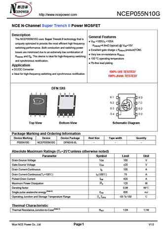
http //www.ncepower.com NCEP055N10G NCE N-Channel Super Trench II Power MOSFET Description General Features The NCEP055N10G uses Super Trench II technology that is VDS =100V,ID =105A uniquely optimized to provide the most efficient high frequency RDS(ON)=4.9m (typical) @ VGS=10V switching performance. Both conduction and switching power Excellent gate charge x RDS(on
9.23. Size:790K ncepower
ncep055n10m.pdf 

NCEP055N10M, NCEP055N10MD NCE N-Channel Super Trench II Power MOSFET Description The series of devices uses Super Trench II technology that is General Features uniquely optimized to provide the most efficient high frequency V =100V,I =110A DS D switching performance. Both conduction and switching power R =5.4m , typical (TO-220)@ V =10V DS(ON) GS losses are minimized due to an e
9.24. Size:405K ncepower
ncep055n10d.pdf 

NCEP055N10, NCEP055N10D NCE N-Channel Super Trench II Power MOSFET Description The series of devices uses Super Trench II technology that is General Features uniquely optimized to provide the most efficient high frequency VDS =100V,ID =110A switching performance. Both conduction and switching power RDS(ON)=5.4m , typical (TO-220)@ VGS=10V losses are minimized due to an ex
9.25. Size:405K ncepower
ncep055n10 ncep055n10d.pdf 

NCEP055N10, NCEP055N10D NCE N-Channel Super Trench II Power MOSFET Description The series of devices uses Super Trench II technology that is General Features uniquely optimized to provide the most efficient high frequency VDS =100V,ID =110A switching performance. Both conduction and switching power RDS(ON)=5.4m , typical (TO-220)@ VGS=10V losses are minimized due to an ex
9.26. Size:358K ncepower
ncep055n12d.pdf 

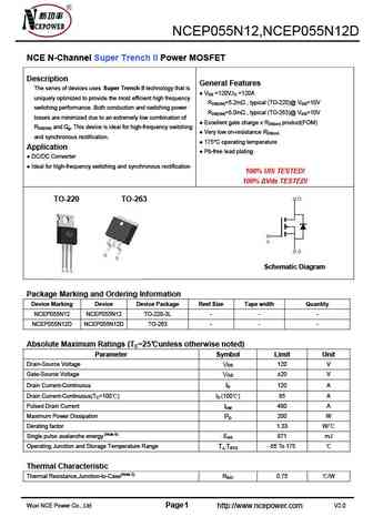
NCEP055N12,NCEP055N12D NCE N-Channel Super Trench II Power MOSFET Description General Features The series of devices uses Super Trench II technology that is VDS =120V,ID =120A uniquely optimized to provide the most efficient high frequency RDS(ON)=5.2m , typical (TO-220)@ VGS=10V switching performance. Both conduction and switching power RDS(ON)=5.0m , typical (TO-263
9.27. Size:1315K ncepower
ncep050n12 ncep050n12d.pdf 

Pb Free Product NCEP050N12, NCEP050N12D NCE N-Channel Super Trench II Power MOSFET Description General Features The series of devices uses Super Trench II technology that is V =120V,I =130A DS D uniquely optimized to provide the most efficient high frequency R =4.5m , typical (TO-220)@ V =10V DS(ON) GS switching performance. Both conduction and switching power R =4.3m , typi
9.28. Size:326K ncepower
ncep050n85g.pdf 

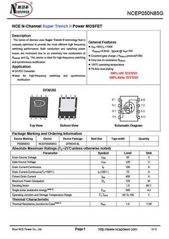
NCEP050N85G NCE N-Channel Super Trench II Power MOSFET Description The series of devices uses Super Trench II technology that is General Features uniquely optimized to provide the most efficient high frequency VDS =85V,ID =100A switching performance. Both conduction and switching power RDS(ON)=4.6m , typical @ VGS=10V losses are minimized due to an extremely low combina
9.29. Size:625K ncepower
ncep058n85m.pdf 

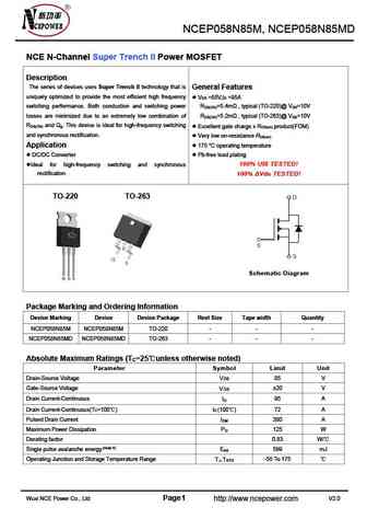
NCEP058N85M, NCEP058N85MD NCE N-Channel Super Trench II Power MOSFET Description The series of devices uses Super Trench II technology that is General Features uniquely optimized to provide the most efficient high frequency V =85V,I =95A DS D switching performance. Both conduction and switching power R =5.4m , typical (TO-220)@ V =10V DS(ON) GS losses are minimized due to an ext
9.30. Size:358K ncepower
ncep055n12.pdf 

NCEP055N12,NCEP055N12D NCE N-Channel Super Trench II Power MOSFET Description General Features The series of devices uses Super Trench II technology that is VDS =120V,ID =120A uniquely optimized to provide the most efficient high frequency RDS(ON)=5.2m , typical (TO-220)@ VGS=10V switching performance. Both conduction and switching power RDS(ON)=5.0m , typical (TO-263
9.31. Size:654K ncepower
ncep050n10mg.pdf 

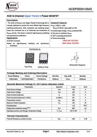
NCEP050N10MG NCE N-Channel Super Trench II Power MOSFET Description The series of devices uses Super Trench II technology that is General Features uniquely optimized to provide the most efficient high frequency V =100V,I =120A DS D switching performance. Both conduction and switching power R =4.45m , typical @ V =10V DS(ON) GS losses are minimized due to an extremely low combina
9.32. Size:342K ncepower
ncep055n85d.pdf 

NCEP055N85, NCEP055N85D NCE N-Channel Super Trench II Power MOSFET Description The series of devices uses Super Trench II technology that is General Features uniquely optimized to provide the most efficient high frequency VDS =85V,ID =100A switching performance. Both conduction and switching power RDS(ON)=4.8m , typical (TO-220)@ VGS=10V losses are minimized due to an ext
9.33. Size:358K ncepower
ncep055n12 ncep055n12d.pdf 

NCEP055N12,NCEP055N12D NCE N-Channel Super Trench II Power MOSFET Description General Features The series of devices uses Super Trench II technology that is VDS =120V,ID =120A uniquely optimized to provide the most efficient high frequency RDS(ON)=5.2m , typical (TO-220)@ VGS=10V switching performance. Both conduction and switching power RDS(ON)=5.0m , typical (TO-263
9.34. Size:286K ncepower
ncep055n12g.pdf 

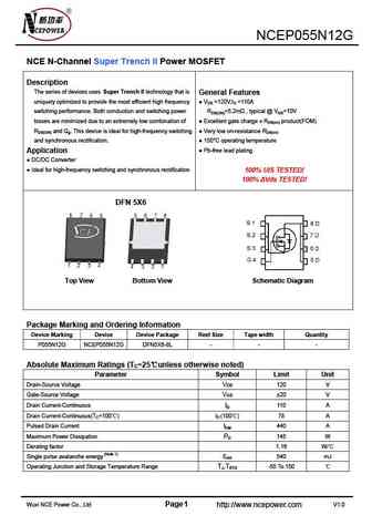
NCEP055N12G NCE N-Channel Super Trench II Power MOSFET Description The series of devices uses Super Trench II technology that is General Features uniquely optimized to provide the most efficient high frequency VDS =120V,ID =110A switching performance. Both conduction and switching power RDS(ON)=5.2m , typical @ VGS=10V losses are minimized due to an extremely low combination
9.35. Size:952K ncepower
ncep050n10md.pdf 

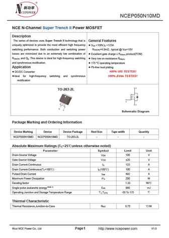
NCEP050N10MD NCE N-Channel Super Trench II Power MOSFET Description The series of devices uses Super Trench II technology that is General Features uniquely optimized to provide the most efficient high frequency V =100V,I =123A DS D switching performance. Both conduction and switching power R =4.0m , typical @ V =10V DS(ON) GS losses are minimized due to an extremely low combinat
9.36. Size:326K ncepower
ncep058n85 ncep058n85d.pdf 

NCEP058N85, NCEP058N85D NCE N-Channel Super Trench II Power MOSFET Description The series of devices uses Super Trench II technology that is General Features uniquely optimized to provide the most efficient high frequency VDS =85V,ID =95A switching performance. Both conduction and switching power RDS(ON)=5.4m , typical (TO-220)@ VGS=10V losses are minimized due to an extr
9.37. Size:304K ncepower
ncep050n12agu.pdf 

NCEP050N12AGU NCE N-Channel Super Trench II Power MOSFET Description General Features The series of devices uses Super Trench II technology that is VDS =120V,ID =120A uniquely optimized to provide the most efficient high frequency RDS(ON)=4.7m , typical @ VGS=10V switching performance. Both conduction and switching power RDS(ON)=6.0m , typical @ VGS=4.5V losses are
Otros transistores... CEM6867, CEM8311, CEM8435A, CEM9407A, CEM9435, CEM9435A, CEM9953A, CEN2301, EMB04N03H, CEP12P10, CEP14P20, CEP15P15, CEP20P06, CEP20P10, CEP30P03, CEP35P10, CEP50P03
