CES2307 MOSFET Equivalente. Reemplazo. Hoja de especificaciones. Principales características
Número de Parte: CES2307
Tipo de FET: MOSFET
Polaridad de transistor: P
ESPECIFICACIONES MÁXIMAS
Pdⓘ - Máxima
disipación de potencia: 1.25 W
|Vds|ⓘ - Voltaje máximo drenador-fuente: 30 V
|Vgs|ⓘ - Voltaje máximo fuente-puerta: 20 V
|Id|ⓘ - Corriente continua
de drenaje: 3.2 A
Tjⓘ - Temperatura máxima de unión: 150 °C
CARACTERÍSTICAS ELÉCTRICAS
trⓘ - Tiempo
de subida: 5 nS
Cossⓘ - Capacitancia de salida: 130 pF
RDSonⓘ - Resistencia estado encendido drenaje a fuente: 0.078 Ohm
Encapsulados: SOT23
Búsqueda de reemplazo de CES2307 MOSFET
- Selecciónⓘ de transistores por parámetros
CES2307 datasheet
..1. Size:493K cet
ces2307.pdf 
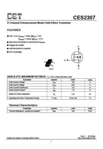
CES2307 P-Channel Enhancement Mode Field Effect Transistor FEATURES -30V, -3.2A, RDS(ON) = 78m @VGS = -10V. RDS(ON) = 120m @VGS = -4.5V. High dense cell design for extremely low RDS(ON). Rugged and reliable. D Lead free product is acquired. SOT-23 package. G D S G S SOT-23 ABSOLUTE MAXIMUM RATINGS TA = 25 C unless otherwise noted Parameter Symbol Limit Units Drain-Sourc
..2. Size:870K cn vbsemi
ces2307.pdf
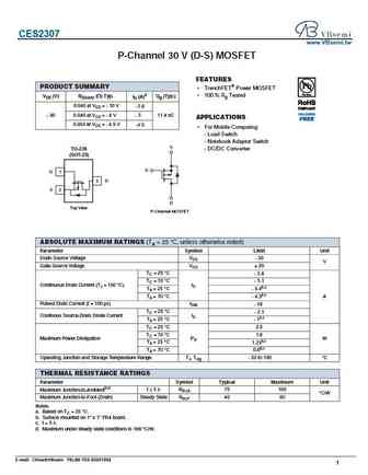
CES2307 www.VBsemi.tw P-Channel 30 V (D-S) MOSFET FEATURES PRODUCT SUMMARY TrenchFET Power MOSFET 100 % Rg Tested VDS (V) RDS(on) ( ) Typ. ID (A)a Qg (Typ.) 0.046 at VGS = - 10 V - 5.6 0.049 at VGS = - 6 V - 5 11.4 nC - 30 APPLICATIONS 0.054 at VGS = - 4.5 V -4.5 For Mobile Computing - Load Switch - Notebook Adaptor Switch S TO-236 - DC/DC Converter (SOT-23)
0.1. Size:424K cet
ces2307a.pdf
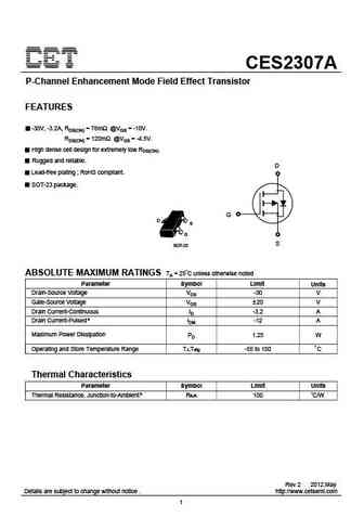
CES2307A P-Channel Enhancement Mode Field Effect Transistor FEATURES -30V, -3.2A, RDS(ON) = 78m @VGS = -10V. RDS(ON) = 120m @VGS = -4.5V. High dense cell design for extremely low RDS(ON). Rugged and reliable. D Lead-free plating ; RoHS compliant. SOT-23 package. G D S G S SOT-23 ABSOLUTE MAXIMUM RATINGS TA = 25 C unless otherwise noted Parameter Symbol Limit Units Drain
8.1. Size:395K cet
ces2301.pdf

CES2301 P-Channel Enhancement Mode Field Effect Transistor FEATURES -20V, -2.8A, RDS(ON) = 100m @VGS = -4.5V. RDS(ON) = 150m @VGS = -2.5V. High dense cell design for extremely low RDS(ON). Rugged and reliable. D Lead free product is acquired. SOT-23 package. G D S G S SOT-23 ABSOLUTE MAXIMUM RATINGS TA = 25 C unless otherwise noted Parameter Symbol Limit Units Drain-Sou
8.2. Size:405K cet
ces2302.pdf
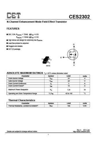
CES2302 N-Channel Enhancement Mode Field Effect Transistor FEATURES 20V, 3.0A, RDS(ON) = 72m @VGS = 4.5V. RDS(ON) = 110m @VGS = 2.5V. High dense cell design for extremely low RDS(ON). Lead free product is acquired. D Rugged and reliable. SOT-23 package. G D S G S SOT-23 ABSOLUTE MAXIMUM RATINGS TA = 25 C unless otherwise noted Parameter Symbol Limit Units Drain-Source V
8.3. Size:132K cet
ces2303.pdf
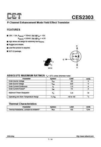
CES2303 P-Channel Enhancement Mode Field Effect Transistor FEATURES -30V, -1.9A, RDS(ON) = 150m (typ) @VGS = -10V. RDS(ON) = 230m (typ) @VGS = -4.5V. High dense cell design for extremely low RDS(ON). Rugged and reliable. D Lead free product is acquired. SOT-23 package. G D S G S SOT-23 ABSOLUTE MAXIMUM RATINGS TA = 25 C unless otherwise noted Parameter Symbol Limit Units
8.4. Size:156K cet
ces2308.pdf

CES2308 N-Channel Enhancement Mode Field Effect Transistor PRELIMINARY FEATURES 20V, 5.4A, RDS(ON) = 27m @VGS = 4.5V. RDS(ON) = 36m @VGS = 2.5V. High dense cell design for extremely low RDS(ON). Rugged and reliable. D Lead free product is acquired. SOT-23 package. G D S G S SOT-23 ABSOLUTE MAXIMUM RATINGS TA = 25 C unless otherwise noted Parameter Symbol Limit Units Drai
8.5. Size:560K cet
ces2306.pdf
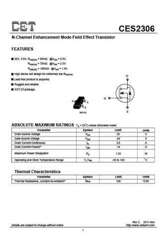
CES2306 N-Channel Enhancement Mode Field Effect Transistor FEATURES 20V, 3.6A, RDS(ON) = 60m @VGS = 4.5V. RDS(ON) = 70m @VGS = 2.5V. RDS(ON) = 100m @VGS = 1.8V. High dense cell design for extremely low RDS(ON). D Lead free product is acquired. Rugged and reliable. SOT-23 package. G D S G S SOT-23 ABSOLUTE MAXIMUM RATINGS TA = 25 C unless otherwise noted Parameter Sy
8.6. Size:156K cet
ces2308(esd).pdf
_0001.jpg)
CES2308 N-Channel Enhancement Mode Field Effect Transistor PRELIMINARY FEATURES 20V, 5.4A, RDS(ON) = 27m @VGS = 4.5V. RDS(ON) = 36m @VGS = 2.5V. High dense cell design for extremely low RDS(ON). Rugged and reliable. D Lead free product is acquired. SOT-23 package. G D S G S SOT-23 ABSOLUTE MAXIMUM RATINGS TA = 25 C unless otherwise noted Parameter Symbol Limit Units Drai
8.7. Size:265K cet
ces2305.pdf
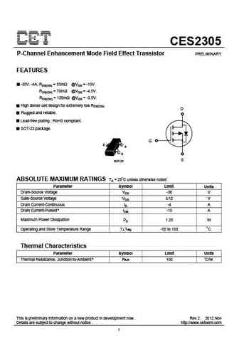
CES2305 P-Channel Enhancement Mode Field Effect Transistor PRELIMINARY FEATURES -30V, -4A, RDS(ON) = 55m @VGS = -10V. RDS(ON) = 70m @VGS = -4.5V. RDS(ON) = 120m @VGS = -2.5V. High dense cell design for extremely low RDS(ON). D Rugged and reliable. Lead-free plating ; RoHS compliant. SOT-23 package. G D S G S SOT-23 ABSOLUTE MAXIMUM RATINGS TA = 25 C unless otherwise
8.8. Size:133K cet
ces2309.pdf
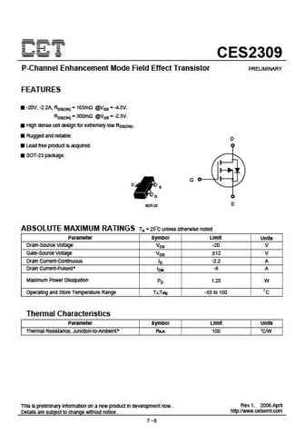
CES2309 P-Channel Enhancement Mode Field Effect Transistor PRELIMINARY FEATURES -20V, -2.2A, RDS(ON) = 165m @VGS = -4.5V. RDS(ON) = 300m @VGS = -2.5V. High dense cell design for extremely low RDS(ON). Rugged and reliable. D Lead free product is acquired. SOT-23 package. G D S G S SOT-23 ABSOLUTE MAXIMUM RATINGS TA = 25 C unless otherwise noted Parameter Symbol Limit Unit
8.9. Size:870K cn vbsemi
ces2301.pdf
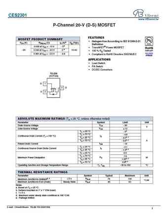
CES2301 www.VBsemi.tw P-Channel 20-V (D-S) MOSFET FEATURES MOSFET PRODUCT SUMMARY Halogen-free According to IEC 61249-2-21 VDS (V) RDS(on) ( )ID (A)a Qg (Typ.) Definition 0.035 at VGS = - 10 V - 5e TrenchFET Power MOSFET e - 20 0.043 at VGS = - 4.5 V - 5 10 nC 100 % Rg Tested 0.061 at VGS = - 2.5 V - 4.8 Compliant to RoHS Directive 2002/95/EC APPLICATIONS
8.10. Size:1706K cn vbsemi
ces2302.pdf
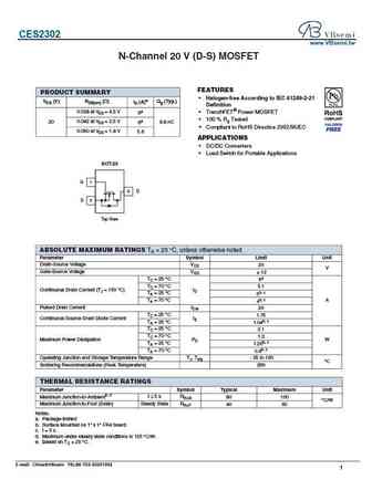
CES2302 www.VBsemi.tw N-Channel 20 V (D-S) MOSFET FEATURES PRODUCT SUMMARY Halogen-free According to IEC 61249-2-21 VDS (V) RDS(on) ( ) ID (A)e Qg (Typ.) Definition 0.028 at VGS = 4.5 V TrenchFET Power MOSFET 6a 100 % Rg Tested 20 0.042 at VGS = 2.5 V 6a 8.8 nC Compliant to RoHS Directive 2002/95/EC 0.050 at VGS = 1.8 V 5.6 APPLICATIONS DC/DC C
Otros transistores... CEP30P03, CEP35P10, CEP50P03, CEP6601, CEP95P04, CES2301, CES2303, CES2305, IRF540N, CES2307A, CES2309, CES2313, CES2313A, CES2317, CES2321, CES2321A, CES2323
