MMBFJ201 Datasheet. Equivalente. Reemplazo. Hoja de especificaciones. Principales características
Número de Parte: MMBFJ201 📄📄
Tipo de FET: JFET
Polaridad de transistor: N
ESPECIFICACIONES MÁXIMAS
Pdⓘ - Máxima disipación de potencia: 0.35 W
|Vds|ⓘ - Voltaje máximo drenador-fuente: 40 V
|Vgs|ⓘ - Voltaje máximo fuente-puerta: 1.5 V
|Id|ⓘ - Corriente continua de drenaje: 0.001 A
Tjⓘ - Temperatura máxima de unión: 150 °C
CARACTERÍSTICAS ELÉCTRICAS
Encapsulados: SOT-23
📄📄 Copiar
Búsqueda de reemplazo de MMBFJ201 MOSFET
- Selecciónⓘ de transistores por parámetros
MMBFJ201 datasheet
..1. Size:783K fairchild semi
j201 j202 mmbfj201 mmbfj202 mmbfj203.pdf 
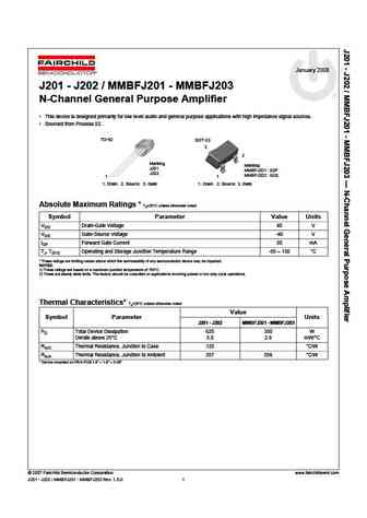
January 2008 J201 - J202 / MMBFJ201 - MMBFJ203 N-Channel General Purpose Amplifier This device is designed primarily for low level audio and general purpose applications with high impedance signal sources. Sourced from Process 52. TO-92 SOT-23 3 2 Marking Marking J201 MMBFJ201 62P J202 MMBFJ202 62Q 1 1 1. Drain 2. Source 3. Gate 1. Drain 2. Source 3. Gate Absolute
8.1. Size:407K fairchild semi
mmbfj270.pdf
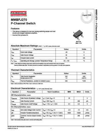
August 2008 MMBFJ270 P-Channel Switch Features This device is designed for low level analog switching sample and hold G circuits and chopper stabilized amplifiers. Sourced from process 88. S D SOT-23 Mark 61S Absolute Maximum Ratings (Note1) Ta = 25 C unless otherwise noted Symbol Parameter Value Units VDG Drain-Gate Voltage -30 V VGS Gate-Source Voltage 30 V IGF Fo
8.2. Size:191K fairchild semi
mmbfj271.pdf
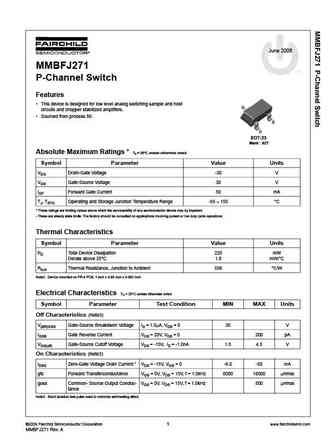
June 2006 MMBFJ271 tm P-Channel Switch Features This device is designed for low level analog switching sample and hold G circuits and chopper stabilized amplifiers. Sourced from process 88. S D SOT-23 Mark 62T Absolute Maximum Ratings * Ta = 25 C unless otherwise noted Symbol Parameter Value Units VDG Drain-Gate Voltage -30 V VGS Gate-Source Voltage 30 V IGF Forwar
9.1. Size:165K motorola
mmbfj309 mmbfj310.pdf
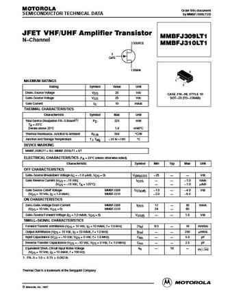
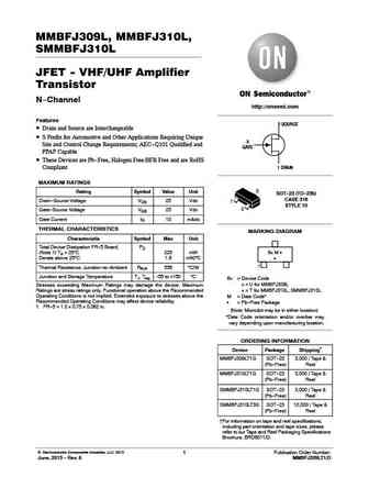
MOTOROLA Order this document SEMICONDUCTOR TECHNICAL DATA by MMBFJ309LT1/D JFET VHF/UHF Amplifier Transistor MMBFJ309LT1 N Channel 2 SOURCE MMBFJ310LT1 3 GATE 1 DRAIN 3 1 MAXIMUM RATINGS 2 Rating Symbol Value Unit Drain Source Voltage VDS 25 Vdc CASE 318 08, STYLE 10 Gate Source Voltage VGS 25 Vdc SOT 23 (TO 236AB) Gate Current IG 10 mAdc THERMAL CHARACTERISTICS
9.2. Size:76K motorola
mmbfj175.pdf
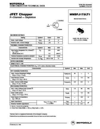
MOTOROLA Order this document SEMICONDUCTOR TECHNICAL DATA by MMBFJ175LT1/D JFET Chopper MMBFJ175LT1 P Channel Depletion Motorola Preferred Device 2 SOURCE 3 GATE 3 1 DRAIN 1 2 MAXIMUM RATINGS Rating Symbol Value Unit CASE 318 08, STYLE 10 SOT 23 (TO 236AB) Drain Gate Voltage VDG 25 V Reverse Gate Source Voltage VGS(r) 25 V THERMAL CHARACTERISTICS Charact
9.3. Size:56K motorola
mmbfj175lt1rev0d.pdf

MOTOROLA Order this document SEMICONDUCTOR TECHNICAL DATA by MMBFJ175LT1/D JFET Chopper MMBFJ175LT1 P Channel Depletion Motorola Preferred Device 2 SOURCE 3 GATE 3 1 DRAIN 1 2 MAXIMUM RATINGS Rating Symbol Value Unit CASE 318 08, STYLE 10 SOT 23 (TO 236AB) Drain Gate Voltage VDG 25 V Reverse Gate Source Voltage VGS(r) 25 V THERMAL CHARACTERISTICS Charact
9.4. Size:57K motorola
mmbfj177lt1rev0d.pdf
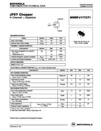
MOTOROLA Order this document SEMICONDUCTOR TECHNICAL DATA by MMBFJ177LT1/D JFET Chopper P Channel Depletion MMBFJ177LT1 2 SOURCE 3 GATE 1 DRAIN 3 1 MAXIMUM RATINGS 2 Rating Symbol Value Unit Drain Gate Voltage VDG 25 Vdc CASE 318 08, STYLE 10 SOT 23 (TO 236AB) Reverse Gate Source Voltage VGS(r) 25 Vdc THERMAL CHARACTERISTICS Characteristic Symbol Max Unit
9.5. Size:128K fairchild semi
mmbfj108.pdf

J108/J109/J110/MMBFJ108 N-Channel Switch 3 This device is designed for digital switching applications where very low on resistance is mandatory. 2 Sourced from Process 58. TO-92 1 SuperSOT-3 1 Marking I8 1. Drain 2. Source 3. Gate 1. Drain 2. Source 3. Gate Absolute Maximum Ratings * TA=25 C unless otherwise noted Symbol Parameter Value Units VDG Drain-Gate Voltage 25
9.6. Size:207K fairchild semi
j309 j310 mmbfj309 mmbfj310.pdf
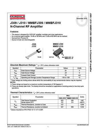
December 2010 J309 / J310 / MMBFJ309 / MMBFJ310 N-Channel RF Amplifier Features This device is designed for VHF/UHF amplifier, oscillator and mixer applications. As a common gate amplifier, 16 dB at 100 MHz and 12 dB at 450 MHz can be realized. Sourced from Process 92. Source & Drain are interchangeable. J309 MMBFJ309 J310 MMBFJ310 G S SOT-23 G TO-92 Mark MMBFJ309
9.7. Size:120K fairchild semi
mmbfj305.pdf
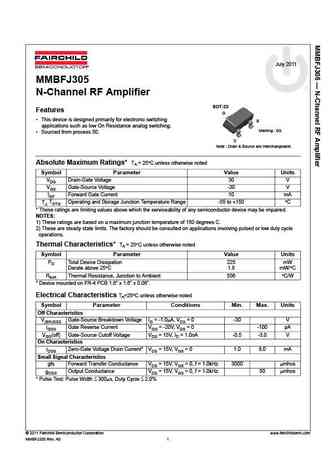
July 2011 MMBFJ305 N-Channel RF Amplifier SOT-23 Features G This device is designed primarily for electronic switching S applications such as low On Resistance analog switching. Marking 6Q Sourced from process 50. D Note Drain & Source are interchangeable. Absolute Maximum Ratings* TA = 25 C unless otherwise noted Symbol Parameter Value Units VDG Drain-Gate Voltage
9.8. Size:728K fairchild semi
j174 j175 j176 j177 mmbfj175 mmbfj176 mmbfj177.pdf
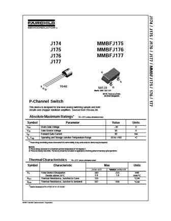
J174 MMBFJ175 J175 MMBFJ176 J176 MMBFJ177 J177 G S S TO-92 D SOT-23 G D Mark 6W / 6X / 6Y NOTE Source & Drain are interchangeable P-Channel Switch This device is designed for low level analog switching sample and hold circuits and chopper stabilized amplifiers. Sourced from Process 88. Absolute Maximum Ratings* TA = 25 C unless otherwise noted Symbol Parameter Value Units
9.9. Size:129K fairchild semi
j108 j109 j110 mmbfj108.pdf
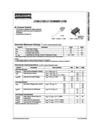
J108/J109/J110/MMBFJ108 N-Channel Switch 3 This device is designed for digital switching applications where very low on resistance is mandatory. 2 Sourced from Process 58. TO-92 1 SuperSOT-3 1 Marking I8 1. Drain 2. Source 3. Gate 1. Drain 2. Source 3. Gate Absolute Maximum Ratings * TA=25 C unless otherwise noted Symbol Parameter Value Units VDG Drain-Gate Voltage 25
9.10. Size:178K fairchild semi
mmbfj110.pdf
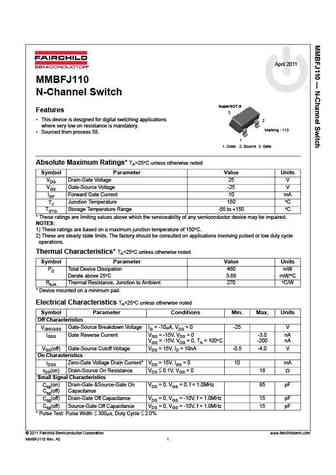
April 2011 MMBFJ110 N-Channel Switch SuperSOT-3 Features 3 This device is designed for digital switching applications 2 where very low on resistance is mandatory. Marking 110 Sourced from process 58. 1 1. Drain 2. Source 3. Gate Absolute Maximum Ratings* TA=25 C unless otherwise noted Symbol Parameter Value Units VDG Drain-Gate Voltage 25 V VGS Gate-Source Voltage -
9.11. Size:151K fairchild semi
mmbfj111 mmbfj112 mmbfj113.pdf
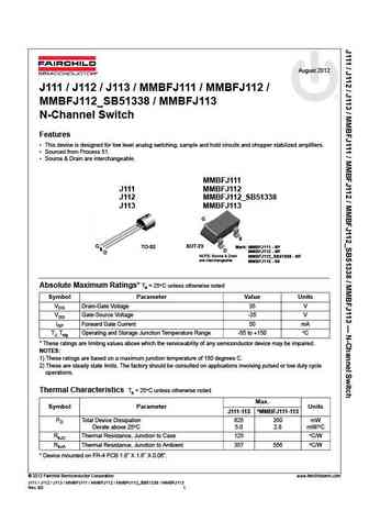
August 2012 J111 / J112 / J113 / MMBFJ111 / MMBFJ112 / MMBFJ112_SB51338 / MMBFJ113 N-Channel Switch Features This device is designed for low level analog switching, sample and hold circuits and chopper stabilized amplifiers. Sourced from Process 51. Source & Drain are interchangeable. MMBFJ111 J111 MMBFJ112 J112 MMBFJ112_SB51338 J113 MMBFJ113 G S SOT-23 G TO-92 Mark
9.12. Size:488K fairchild semi
j111 j112 j113 mmbfj111 mmbfj112 mmbfj113.pdf
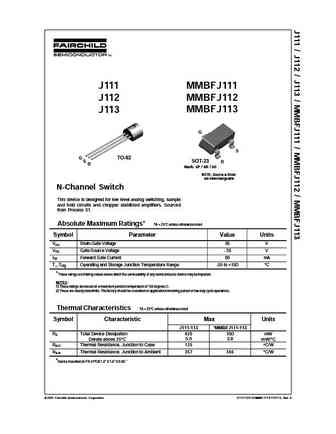
J111 MMBFJ111 J112 MMBFJ112 J113 MMBFJ113 G S G TO-92 S SOT-23 D D Mark 6P / 6R / 6S NOTE Source & Drain are interchangeable N-Channel Switch This device is designed for low level analog switching, sample and hold circuits and chopper stabilized amplifiers. Sourced from Process 51. Absolute Maximum Ratings* TA = 25 C unless otherwise noted Symbol Parameter Value Units VDG D
9.13. Size:152K fairchild semi
mmbfj310.pdf
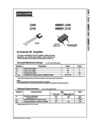
J309 MMBFJ309 J310 MMBFJ310 G S G TO-92 S SOT-23 NOTE Source & Drain D D are interchangeable Mark 6U / 6T N-Channel RF Amplifier This device is designed for VHF/UHF amplifier, oscillator and mixer applications. As a common gate amplifier, 16 dB at 100 MHz and 12 dB at 450 MHz can be realized. Sourced from Process 92. Absolute Maximum Ratings* TA = 25 C unless otherwise noted
9.14. Size:109K onsemi
mmbfj177lt1-d.pdf
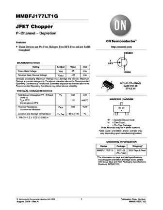
MMBFJ177LT1G JFET Chopper P-Channel - Depletion Features These Devices are Pb-Free, Halogen Free/BFR Free and are RoHS http //onsemi.com Compliant 2 SOURCE 3 MAXIMUM RATINGS GATE Rating Symbol Value Unit Drain-Gate Voltage VDG 25 Vdc 1 DRAIN Reverse Gate-Source Voltage VGS(r) -25 Vdc Stresses exceeding Maximum Ratings may damage the device. Maximum Ratings are stress ratings
9.15. Size:144K onsemi
mmbfj309lt1 mmbfj310lt1.pdf
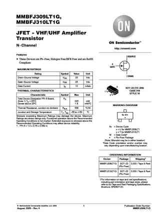
MMBFJ309LT1G, MMBFJ310LT1G JFET - VHF/UHF Amplifier Transistor N-Channel http //onsemi.com Features 2 SOURCE These Devices are Pb-Free, Halogen Free/BFR Free and are RoHS Compliant 3 GATE MAXIMUM RATINGS Rating Symbol Value Unit 1 DRAIN Drain-Source Voltage VDS 25 Vdc Gate-Source Voltage VGS 25 Vdc Gate Current IG 10 mAdc 3 SOT-23 (TO-236) THERMAL CHARACTERISTICS CASE 31
9.16. Size:101K onsemi
smmbfj310lt1g smmbfj310lt3g.pdf
MMBFJ309L, MMBFJ310L, SMMBFJ310L JFET - VHF/UHF Amplifier Transistor N-Channel http //onsemi.com Features 2 SOURCE Drain and Source are Interchangeable S Prefix for Automotive and Other Applications Requiring Unique 3 Site and Control Change Requirements; AEC-Q101 Qualified and GATE PPAP Capable These Devices are Pb-Free, Halogen Free/BFR Free and are RoHS 1 DRAIN Co
9.17. Size:105K onsemi
mmbfj175lt1.pdf
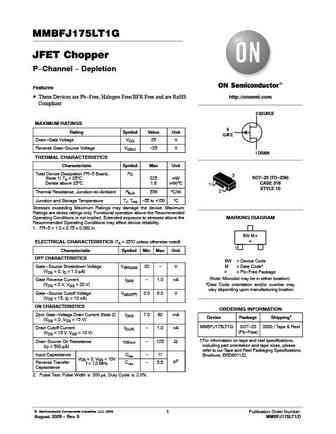
MMBFJ175LT1G JFET Chopper P-Channel - Depletion Features These Devices are Pb-Free, Halogen Free/BFR Free and are RoHS http //onsemi.com Compliant 2 SOURCE MAXIMUM RATINGS 3 Rating Symbol Value Unit GATE Drain-Gate Voltage VDG 25 V Reverse Gate-Source Voltage VGS(r) -25 V 1 DRAIN THERMAL CHARACTERISTICS Characteristic Symbol Max Unit Total Device Dissipation FR-5 Board, PD
Otros transistores... J175, J176, J177, MMBFJ175, MMBFJ176, MMBFJ177, J201, J202, 20N60, MMBFJ202, J210, MMBFJ210, MMBFJ211, MMBFJ212, J270, J271, J304
