J271 MOSFET Equivalente. Reemplazo. Hoja de especificaciones. Principales características
Número de Parte: J271
Tipo de FET: JFET
Polaridad de transistor: P
ESPECIFICACIONES MÁXIMAS
Pdⓘ - Máxima disipación de potencia: 0.35 W
|Vds|ⓘ - Voltaje máximo drenador-fuente: 30 V
|Vgs|ⓘ - Voltaje máximo fuente-puerta: 4.5 V
|Id|ⓘ - Corriente continua de drenaje: 0.05 A
Tjⓘ - Temperatura máxima de unión: 150 °C
CARACTERÍSTICAS ELÉCTRICAS
RDSonⓘ - Resistencia estado encendido drenaje a fuente: 50 Ohm
Encapsulados: TO-92
Búsqueda de reemplazo de J271 MOSFET
- Selecciónⓘ de transistores por parámetros
J271 datasheet
j271.pdf
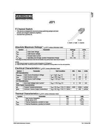
J271 P-Channel Switch This device is designed for low level analog switching sample and hold circuits and chopper stabilized amplifiers. Sourced from process 88. TO-92 1 1. Drain 2. Gate 3. Source Absolute Maximum Ratings* Ta=25 C unless otherwise noted Symbol Parameter Ratings Units VDG Drain-Gate Voltage 30 V VGS Gate-Source Voltage 30 V IGF Forward Gate Current 50 mA
j270 sst270 j271 sst271.pdf
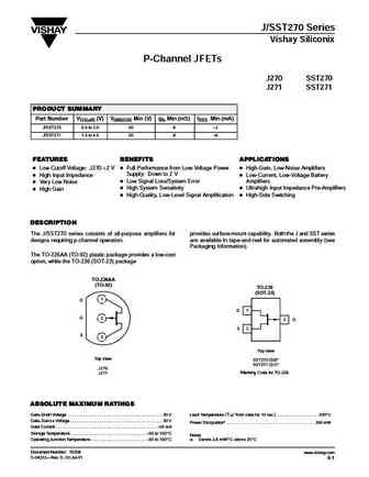
J/SST270 Series Vishay Siliconix P-Channel JFETs J270 SST270 J271 SST271 PRODUCT SUMMARY Part Number VGS(off) (V) V(BR)GSS Min (V) gfs Min (mS) IDSS Min (mA) J/SST270 0.5 to 2.0 30 6 2 J/SST271 1.5 to 4.5 30 8 6 FEATURES BENEFITS APPLICATIONS D Low Cutoff Voltage J270
j270 j271 sst270 sst271.pdf
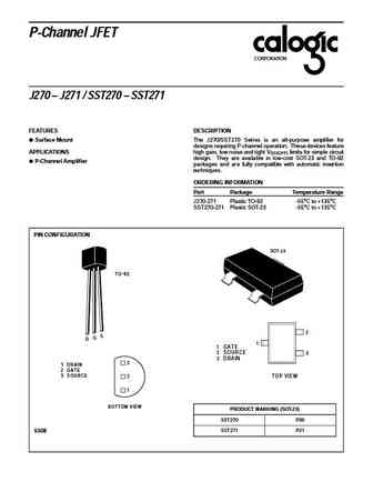
P-Channel JFET CORPORATION J270 J271 / SST270 SST271 FEATURES DESCRIPTION Surface Mount The J270/SST270 Series is an all-purpose amplifier for designs requiring P-channel operation. These devices feature APPLICATIONS high gain, low noise and tight V limits for simple circuit GS(OFF) design. They are available in low-cost SOT-23 and TO-92 P-Channel Amplifier p
mmbfj271.pdf
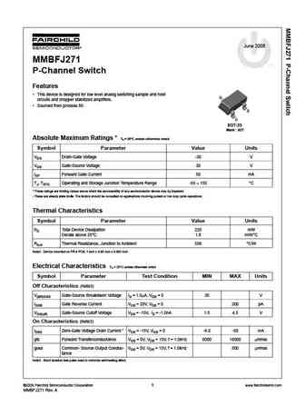
June 2006 MMBFJ271 tm P-Channel Switch Features This device is designed for low level analog switching sample and hold G circuits and chopper stabilized amplifiers. Sourced from process 88. S D SOT-23 Mark 62T Absolute Maximum Ratings * Ta = 25 C unless otherwise noted Symbol Parameter Value Units VDG Drain-Gate Voltage -30 V VGS Gate-Source Voltage 30 V IGF Forwar
Otros transistores... J202 , MMBFJ201 , MMBFJ202 , J210 , MMBFJ210 , MMBFJ211 , MMBFJ212 , J270 , IRF1404 , J304 , J305 , KSK30 , KSK595H , KSK596 , LS4117 , LS4118 , LS4119 .
🌐 : EN ES РУ

Liste
Recientemente añadidas las descripciónes de los transistores:
MOSFET: ASU70R600E | ASU65R850E | ASU65R550E | ASU65R350E | ASR65R120EFD | ASR65R046EFD | ASQ65R046EFD | ASM65R280E | ASM60R330E | ASE70R950E | ASD80R750E | ASD70R950E | ASD70R600E | ASD70R380E | ASD65R850E | ASD65R550E
Popular searches
c945 transistor | irf640n | 2n3904 | bc547 datasheet | k3797 mosfet | bs170 datasheet | tip41c | irfp460