MMBF4093 MOSFET Equivalente. Reemplazo. Hoja de especificaciones. Principales características
Número de Parte: MMBF4093
Tipo de FET: JFET
Polaridad de transistor: N
ESPECIFICACIONES MÁXIMAS
Pdⓘ - Máxima disipación de potencia: 0.35
W
|Vds|ⓘ - Voltaje máximo drenador - fuente: 40
V
|Vgs|ⓘ - Voltaje máximo fuente - puerta: 5
V
|Id|ⓘ - Corriente continua de drenaje: 0.008
A
Tjⓘ - Temperatura máxima de unión: 150
°C
CARACTERÍSTICAS ELÉCTRICAS
Rds(on)ⓘ - Resistencia estado encendido drenaje a fuente: 80
Ohm
Paquete / Cubierta:
SOT-23
Búsqueda de reemplazo de MMBF4093 MOSFET
-
Selección ⓘ de transistores por parámetros
Principales características: MMBF4093
..1. Size:55K fairchild semi
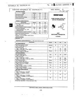
pn4091 pn4092 pn4093 mmbf4091 mmbf4092 mmbf4093.pdf 
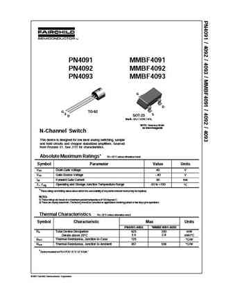
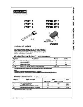
PN4091 MMBF4091 PN4092 MMBF4092 PN4093 MMBF4093 G D G TO-92 S S SOT-23 D Mark 61J / 61K / 61L NOTE Source & Drain are interchangeable N-Channel Switch This device is designed for low level analog switching, sample and hold circuits and chopper stabalized amplifiers. Sourced from Process 51. See J111 for characteristics. Absolute Maximum Ratings* TA = 25 C unless otherwise no
9.2. Size:292K motorola
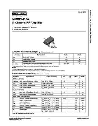
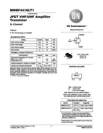
mmbf4416lt1rev0d.pdf 
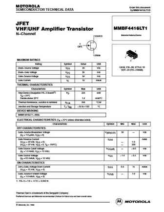
MOTOROLA Order this document SEMICONDUCTOR TECHNICAL DATA by MMBF4416LT1/D JFET MMBF4416LT1 VHF/UHF Amplifier Transistor N Channel Motorola Preferred Device 2 SOURCE 3 GATE 3 1 DRAIN 1 MAXIMUM RATINGS 2 Rating Symbol Value Unit CASE 318 08, STYLE 10 Drain Source Voltage VDS 30 Vdc SOT 23 (TO 236AB) Drain Gate Voltage VDG 30 Vdc Gate Source Voltage VGS 30 Vdc
9.3. Size:139K motorola
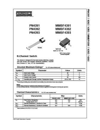
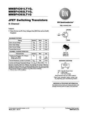
mmbf4391lt1 mmbf4392lt1 mmbf4393lt1.pdf 
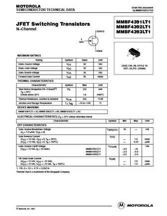
MOTOROLA Order this document SEMICONDUCTOR TECHNICAL DATA by MMBF4391LT1/D MMBF4391LT1 JFET Switching Transistors MMBF4392LT1 N Channel 2 SOURCE MMBF4393LT1 3 GATE 3 1 DRAIN 1 MAXIMUM RATINGS 2 Rating Symbol Value Unit Drain Source Voltage VDS 30 Vdc CASE 318 08, STYLE 10 Drain Gate Voltage VDG 30 Vdc SOT 23 (TO 236AB) Gate Source Voltage VGS 30 Vdc Forward
9.4. Size:128K fairchild semi
pn4117 pn4118 pn4119 mmbf4117 mmbf4118 mmbf4119.pdf 
PN4117 MMBF4117 PN4118 MMBF4118 PN4119 MMBF4119 G S G TO-92 S SOT-23 D D Mark 61A / 61C / 61E NOTE Source & Drain are interchangeable N-Channel Switch This device is designed for low current DC and audio applications. These devices provide excellent performance as input stages for sub-picoamp instrumentation or any high impedance signal sources. Sourced from Process 53. Abso
9.5. Size:49K fairchild semi
mmbf4416a.pdf 
March 2005 MMBF4416A N-Channel RF Amplifier This device is designed for RF amplifiers. Sourced from process 50. G S SOT-23 D Mark 6BG Absolute Maximum Ratings* Ta = 25 C unless otherwise noted Symbol Parameter Value Units VDG Drain-Gate Voltage 35 V VGS Gate-Source Voltage -35 V IGF Forward Gate Current 10 mA TJ, TSTG Operating and Storage Junction Temperature Range - 5
9.6. Size:708K fairchild semi
pn4391 pn4392 pn4393 mmbf4391 mmbf4392 mmbf4393.pdf 
PN4391 MMBF4391 PN4392 MMBF4392 PN4393 MMBF4393 G S G TO-92 S SOT-23 D D Mark 6J / 6K / 6G NOTE Source & Drain are interchangeable N-Channel Switch This device is designed for low level analog switching, sample and hold circuits and chopper stabalized amplifiers. Sourced from Process 51. See J111 for characteristics. Absolute Maximum Ratings* TA = 25 C unless otherwise noted
9.7. Size:100K fairchild semi
mmbf4416.pdf 
April 2009 MMBF4416 N-Channel RF Amplifiers This device is designed for RF amplifiers. G Sourced from process 50. S SOT-23 D Mark 6A Absolute Maximum Ratings TA=25 C unless otherwise noted Symbol Parameter Value Units VDG Drain-Gate Voltage 30 V VGS Gate-Source Voltage -30 V IGF Forward Gate Current 10 mA TJ, TSTG Junction and Storage Temperature Range -55 to +150 C
9.8. Size:279K onsemi
mmbf4391 mmbf4392 mmbf4393.pdf 
Is Now Part of To learn more about ON Semiconductor, please visit our website at www.onsemi.com Please note As part of the Fairchild Semiconductor integration, some of the Fairchild orderable part numbers will need to change in order to meet ON Semiconductor s system requirements. Since the ON Semiconductor product management systems do not have the ability to manage part nomenclatur
9.9. Size:127K onsemi
mmbf4391lt1 mmbf4392lt1g mmbf4393lt1g.pdf 
MMBF4391LT1G, MMBF4392LT1G, MMBF4393LT1G JFET Switching Transistors N-Channel http //onsemi.com Features 2 SOURCE These Devices are Pb-Free, Halogen Free/BFR Free and are RoHS Compliant 3 GATE MAXIMUM RATINGS 1 DRAIN Rating Symbol Value Unit Drain-Source Voltage VDS 30 Vdc Drain-Gate Voltage VDG 30 Vdc 3 Gate-Source Voltage VGS 30 Vdc 1 Forward Gate Current IG(f) 50 mAdc
9.10. Size:149K onsemi
mmbf4416lt1.pdf 
MMBF4416LT1 Preferred Device JFET VHF/UHF Amplifier Transistor N-Channel http //onsemi.com Features Pb-Free Package is Available 2 SOURCE MAXIMUM RATINGS 3 Rating Symbol Value Unit GATE Drain-Source Voltage VDS 30 Vdc Drain-Gate Voltage VDG 30 Vdc 1 DRAIN Gate-Source Voltage VGS 30 Vdc Gate Current IG 10 mAdc THERMAL CHARACTERISTICS 3 SOT-23 (TO-236) Characteristic Sym
Otros transistores... KSK30
, KSK595H
, KSK596
, LS4117
, LS4118
, LS4119
, MMBF4091
, MMBF4092
, 2N7000
, PN4091
, PN4092
, PN4093
, MMBF4117
, MMBF4118
, MMBF4119
, MMBF4391
, MMBF4392
.
History: NTTFS4941NTAG
| IPP050N06NG