8N90 MOSFET Equivalente. Reemplazo. Hoja de especificaciones. Principales características
Número de Parte: 8N90
Tipo de FET: MOSFET
Polaridad de transistor: N
ESPECIFICACIONES MÁXIMAS
Pdⓘ - Máxima
disipación de potencia: 147 W
|Vds|ⓘ - Voltaje máximo drenador-fuente: 900 V
|Vgs|ⓘ - Voltaje máximo fuente-puerta: 30 V
|Id|ⓘ - Corriente continua
de drenaje: 8 A
Tjⓘ - Temperatura máxima de unión: 150 °C
CARACTERÍSTICAS ELÉCTRICAS
trⓘ - Tiempo
de subida: 110 nS
Cossⓘ - Capacitancia de salida: 130 pF
RDSonⓘ - Resistencia estado encendido drenaje a fuente: 1.3 Ohm
Encapsulados: TO-220
Búsqueda de reemplazo de 8N90 MOSFET
- Selecciónⓘ de transistores por parámetros
8N90 datasheet
..1. Size:181K utc
8n90.pdf 
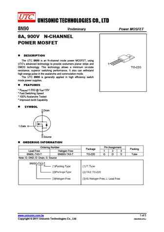
UNISONIC TECHNOLOGIES CO., LTD 8N90 Preliminary Power MOSFET 8A, 900V N-CHANNEL POWER MOSFET DESCRIPTION The UTC 8N90 is an N-channel mode power MOSFET, using UTC s advanced technology to provide costumers planar stripe and DMOS technology. This technology allows a minimum on-state resistance, superior switching performance. It also can withstand high energy pulse in the ava
0.2. Size:865K fairchild semi
fqp8n90c fqpf8n90c.pdf
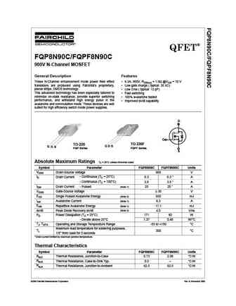
QFET FQP8N90C/FQPF8N90C 900V N-Channel MOSFET General Description Features These N-Channel enhancement mode power field effect 6.3A, 900V, RDS(on) = 1.9 @VGS = 10 V transistors are produced using Fairchild s proprietary, Low gate charge ( typical 35 nC) planar stripe, DMOS technology. Low Crss ( typical 12 pF) This advanced technology has been especially tailored to
0.3. Size:807K fairchild semi
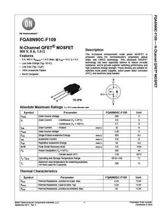
fqa8n90c f109.pdf
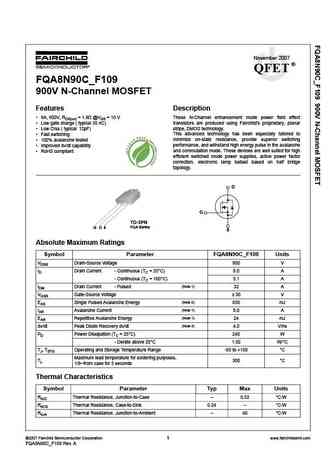
November 2007 QFET FQA8N90C_F109 900V N-Channel MOSFET Features Description 8A, 900V, RDS(on) = 1.9 @VGS = 10 V These N-Channel enhancement mode power field effect Low gate charge ( typical 35 nC) transistors are produced using Fairchild s proprietary, planar stripe, DMOS technology. Low Crss ( typical 12pF) This advanced technology has been especially tailored to
0.4. Size:690K fairchild semi
fqa8n90c.pdf
TM QFET FQA8N90C 900V N-Channel MOSFET General Description Features These N-Channel enhancement mode power field effect 8A, 900V, RDS(on) = 1.9 @VGS = 10 V transistors are produced using Fairchild s proprietary, Low gate charge ( typical 35 nC) planar stripe, DMOS technology. Low Crss ( typical 12 pF) This advanced technology has been especially tailored to Fast s
0.5. Size:430K fairchild semi
fqb8n90ctm.pdf
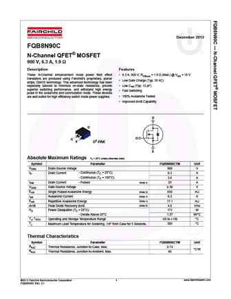
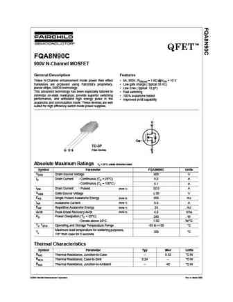
December 2013 FQB8N90C N-Channel QFET MOSFET 900 V, 6.3 A, 1.9 Description Features These N-Channel enhancement mode power field effect 6.3 A, 900 V, RDS(on) = 1.9 (Max.) @ VGS = 10 V transistors are produced using Fairchild s proprietary, planar Low Gate Charge (Typ. 35 nC) stripe, DMOS technology. This advanced technology has been Low Crss (Typ. 12 pF) especia
0.6. Size:935K samsung
ssf8n90a.pdf
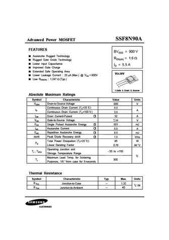
Advanced Power MOSFET FEATURES BVDSS = 900 V Avalanche Rugged Technology RDS(on) = 1.6 Rugged Gate Oxide Technology Lower Input Capacitance ID = 5.5 A Improved Gate Charge Extended Safe Operating Area Lower Leakage Current 25 A (Max.) @ VDS = 900V Low RDS(ON) 1.247 (Typ.) 1 2 3 1.Gate 2. Drain 3. Source Absolute Maximum Ratings Symbol Characteristic Valu
0.7. Size:937K samsung
ssh8n90a.pdf
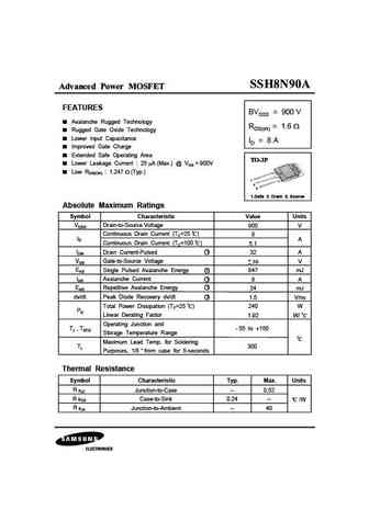
Advanced Power MOSFET FEATURES BVDSS = 900 V Avalanche Rugged Technology RDS(on) = 1.6 Rugged Gate Oxide Technology Lower Input Capacitance ID = 8 A Improved Gate Charge Extended Safe Operating Area Lower Leakage Current 25 A (Max.) @ VDS = 900V Low RDS(ON) 1.247 (Typ.) 1 2 3 1.Gate 2. Drain 3. Source Absolute Maximum Ratings Symbol Characteristic Value
0.8. Size:89K ixys
ixgh28n90b.pdf

IXGH 28N90B VCES = 900 V HiPerFASTTM IGBT IXGT 28N90B IC25 = 51 A VCE(SAT) = 2.7 V Preliminary data sheet tfi(typ) = 130 ns Symbol Test Conditions Maximum Ratings TO-247 AD (IXGH) VCES TJ = 25 C to 150 C 900 V VCGR TJ = 25 C to 150 C; RGE = 1 MW 900 V C (TAB) VGES Continuous 20 V G C VGEM Transient 30 V E IC25 TC = 25 C51 A IC110 TC = 110 C28 A TO-268 (D3) ICM TC =
0.9. Size:178K ixys
ixyp8n90c3.pdf
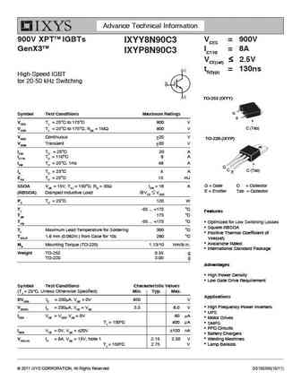
Advance Technical Information 900V XPTTM IGBTs VCES = 900V IXYY8N90C3 GenX3TM IC110 = 8A IXYP8N90C3 VCE(sat) 2.5V tfi(typ) = 130ns High-Speed IGBT for 20-50 kHz Switching TO-252 (IXYY) G Symbol Test Conditions Maximum Ratings E VCES TJ = 25 C to 175 C 900 V C (Tab) VCGR TJ = 25 C to 175 C, RGE = 1M 900 V VGES Continuous 20 V TO-220 (IXYP) VG
0.10. Size:336K ixys
ixya8n90c3d1.pdf

Preliminary Technical Information 900V XPTTM IGBTs VCES = 900V IXYA8N90C3D1 GenX3TM w/Diode IC110 = 8A IXYP8N90C3D1 VCE(sat) 2.5V tfi(typ) = 130ns High-Speed IGBT for 20-50 kHz Switching TO-263 AA (IXYA) G Symbol Test Conditions Maximum Ratings E VCES TJ = 25 C to 175 C 900 V C (Tab) VCGR TJ = 25 C to 175 C, RGE = 1M 900 V VGES Continuous 20 V
0.11. Size:89K ixys
ixgt28n90b.pdf
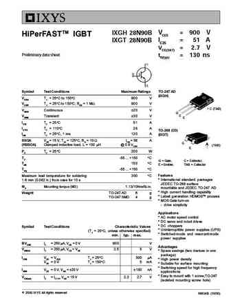
IXGH 28N90B VCES = 900 V HiPerFASTTM IGBT IXGT 28N90B IC25 = 51 A VCE(SAT) = 2.7 V Preliminary data sheet tfi(typ) = 130 ns Symbol Test Conditions Maximum Ratings TO-247 AD (IXGH) VCES TJ = 25 C to 150 C 900 V VCGR TJ = 25 C to 150 C; RGE = 1 MW 900 V C (TAB) VGES Continuous 20 V G C VGEM Transient 30 V E IC25 TC = 25 C51 A IC110 TC = 110 C28 A TO-268 (D3) ICM TC =
0.12. Size:178K ixys
ixyy8n90c3.pdf

Advance Technical Information 900V XPTTM IGBTs VCES = 900V IXYY8N90C3 GenX3TM IC110 = 8A IXYP8N90C3 VCE(sat) 2.5V tfi(typ) = 130ns High-Speed IGBT for 20-50 kHz Switching TO-252 (IXYY) G Symbol Test Conditions Maximum Ratings E VCES TJ = 25 C to 175 C 900 V C (Tab) VCGR TJ = 25 C to 175 C, RGE = 1M 900 V VGES Continuous 20 V TO-220 (IXYP) VG
0.13. Size:336K ixys
ixyp8n90c3d1.pdf
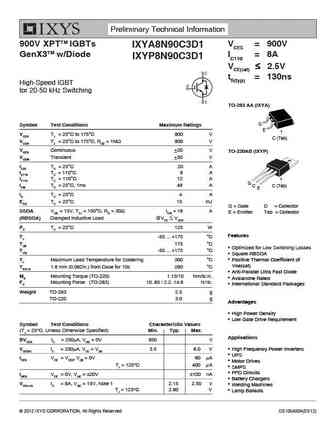
Preliminary Technical Information 900V XPTTM IGBTs VCES = 900V IXYA8N90C3D1 GenX3TM w/Diode IC110 = 8A IXYP8N90C3D1 VCE(sat) 2.5V tfi(typ) = 130ns High-Speed IGBT for 20-50 kHz Switching TO-263 AA (IXYA) G Symbol Test Conditions Maximum Ratings E VCES TJ = 25 C to 175 C 900 V C (Tab) VCGR TJ = 25 C to 175 C, RGE = 1M 900 V VGES Continuous 20 V
0.15. Size:1275K onsemi
fqa8n90c-f109.pdf
FQA8N90C-F109 N-Channel QFET MOSFET Description 900 V, 8 A, 1.9 This N-Channel enhancement mode power MOSFET is Features produced using ON Semiconductor s proprietary planar 8 A, 900 V, RDS(on) = 1.9 (Max.) @ VGS = 10 V, ID = 4 V stripe and DMOS technology. This advanced MOSFET technology has been especially tailored to reduce on-state Low Gate Charge (Typ. 3
0.16. Size:538K onsemi
fqb8n90c.pdf

Is Now Part of To learn more about ON Semiconductor, please visit our website at www.onsemi.com Please note As part of the Fairchild Semiconductor integration, some of the Fairchild orderable part numbers will need to change in order to meet ON Semiconductor s system requirements. Since the ON Semiconductor product management systems do not have the ability to manage part nomenclatur
0.17. Size:647K crhj
cs8n90 a8.pdf
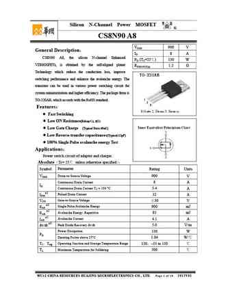
Silicon N-Channel Power MOSFET R CS8N90 A8 VDSS 900 V General Description ID 8 A CS8N90 A8, the silicon N-channel Enhanced PD (TC=25 ) 130 W VDMOSFETs, is obtained by the self-aligned planar RDS(ON)Typ 1.2 Technology which reduce the conduction loss, improve switching performance and enhance the avalanche energy. The transistor can be used in various power sw
0.18. Size:770K crhj
cs8n90f a9hd.pdf

Silicon N-Channel Power MOSFET R CS8N90F A9HD VDSS 900 V General Description ID 8 A CS8N90F A9HD, the silicon N-channel Enhanced PD (TC=25 ) 57 W VDMOSFETs, is obtained by the self-aligned planar RDS(ON)Typ 1.3 Technology which reduce the conduction loss, improve switching performance and enhance the avalanche energy. The transistor can be used in various
0.19. Size:652K crhj
cs8n90f a9.pdf
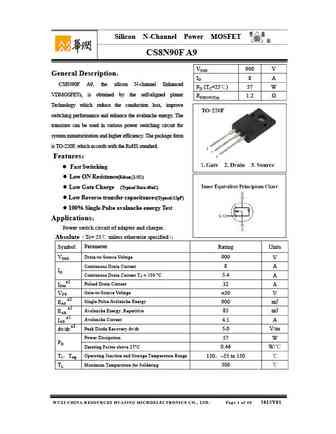
Silicon N-Channel Power MOSFET R CS8N90F A9 VDSS 900 V General Description ID 8 A CS8N90F A9, the silicon N-channel Enhanced PD (TC=25 ) 57 W VDMOSFETs, is obtained by the self-aligned planar RDS(ON)Typ 1.2 Technology which reduce the conduction loss, improve switching performance and enhance the avalanche energy. The transistor can be used in various powe
0.20. Size:614K samwin
swj8n90ku.pdf
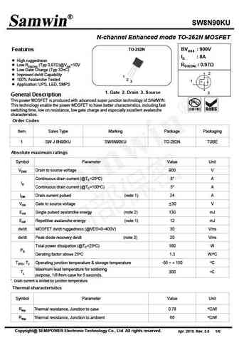
SW8N90KU N-channel Enhanced mode TO-262N MOSFET TO-262N BVDSS 900V Features ID 8A High ruggedness RDS(ON) 0.97 Low RDS(ON) (Typ 0.97 )@VGS=10V Low Gate Charge (Typ 32nC) 2 Improved dv/dt Capability 1 100% Avalanche Tested 2 1 3 Application UPS, LED, SMPS 1. Gate 2. Drain 3. Source 3 General Description This power MOSFET
0.21. Size:1305K way-on
wmj18n90d1.pdf
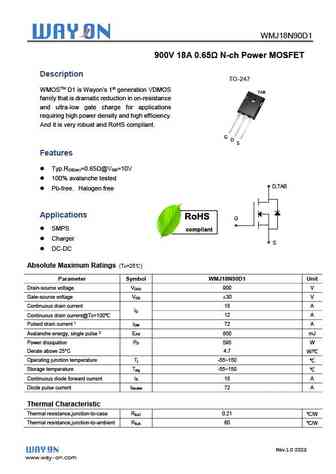
WMJ18N90D1 900V 18A 0.65 N-ch Power MOSFET Description TO-247 WMOSTM D1 is Wayon s 1st generation VDMOS TAB family that is dramatic reduction in on-resistance and ultra-low gate charge for applications requiring high power density and high efficiency. And it is very robust and RoHS compliant. G D S Features Typ.R =0.65 @V =10V DS(on) GS 100% avalanc
0.22. Size:770K wuxi china
cs8n90fa9hd.pdf

Silicon N-Channel Power MOSFET R CS8N90F A9HD VDSS 900 V General Description ID 8 A CS8N90F A9HD, the silicon N-channel Enhanced PD (TC=25 ) 57 W VDMOSFETs, is obtained by the self-aligned planar RDS(ON)Typ 1.3 Technology which reduce the conduction loss, improve switching performance and enhance the avalanche energy. The transistor can be used in various
0.23. Size:666K convert
cs8n90f cs8n90p.pdf
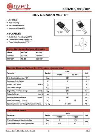
nvert Suzhou Convert Semiconductor Co ., Ltd. CS8N90F, CS8N90P 900V N-Channel MOSFET FEATURES Fast switching 100% avalanche tested Improved dv/dt capability APPLICATIONS Switch Mode Power Supply (SMPS) Uninterruptible Power Supply (UPS) Power Factor Correction (PFC) Device Marking and Package Information Device Package Marking CS8N90F TO-220F CS8N90F CS8N9
0.24. Size:581K cn scilicon
sfp070n90c3 sfb068n90c3.pdf
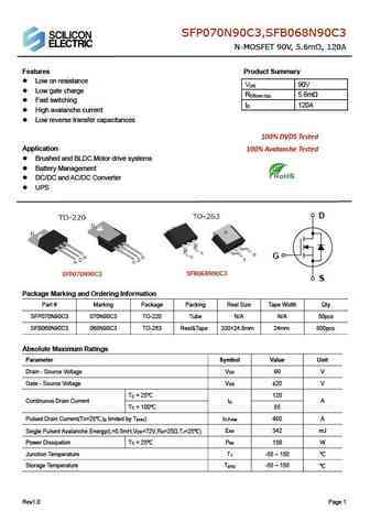
SFP070N90C3,SFB068N90C3 N-MOSFET 90V, 5.6m , 120A Features Product Summary Low on resistance V 90V DS Low gate charge R 5.6m DS(on) typ. Fast switching I 120A D High avalanche current Low reverse transfer capacitances 100% DVDS Tested Application 100% Avalanche Tested Brushed and BLDC Motor drive systems Battery Management DC/DC and A
0.25. Size:217K inchange semiconductor
8n90a.pdf
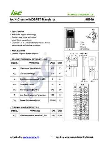
isc N-Channel MOSFET Transistor 8N90A DESCRIPTION Avalanche rugged technology Rugged gate oxide technology Lower input capacitance Minimum Lot-to-Lot variations for robust device performance and reliable operation APPLICATIONS General purpose power amplifier ABSOLUTE MAXIMUM RATINGS(T =25 ) C SYMBOL PARAMETER VALUE UNIT V Drain-Source Voltage (V =0) 900 V DSS GS
Otros transistores... STK001SF
, STK003SF
, STK004SF
, SUF1002
, SUF2001
, SUF3001
, SUM201MN
, SUM202MN
, IRF1404
, 9N90
, 10N90
, 11N90
, 12N90
, 9N95
, 9N100
, 1N90
, 2N90
.