9N90 Datasheet. Equivalente. Reemplazo. Hoja de especificaciones. Principales características
Número de Parte: 9N90 📄📄
Tipo de FET: MOSFET
Polaridad de transistor: N
ESPECIFICACIONES MÁXIMAS
Pdⓘ - Máxima disipación de potencia: 240 W
|Vds|ⓘ - Voltaje máximo drenador-fuente: 900 V
|Vgs|ⓘ - Voltaje máximo fuente-puerta: 30 V
|Id|ⓘ - Corriente continua de drenaje: 9 A
Tjⓘ - Temperatura máxima de unión: 150 °C
CARACTERÍSTICAS ELÉCTRICAS
trⓘ - Tiempo de subida: 120 nS
Cossⓘ - Capacitancia de salida: 175 pF
RDSonⓘ - Resistencia estado encendido drenaje a fuente: 1.05 Ohm
📄📄 Copiar
Búsqueda de reemplazo de 9N90 MOSFET
- Selecciónⓘ de transistores por parámetros
9N90 datasheet
9n90.pdf
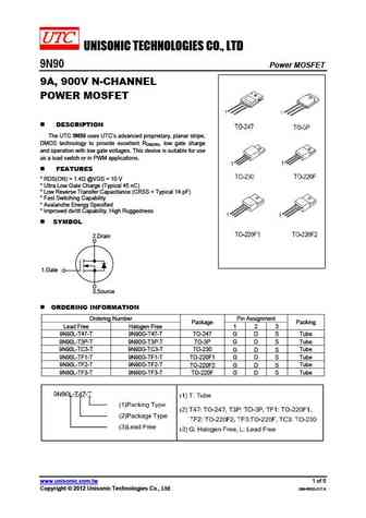
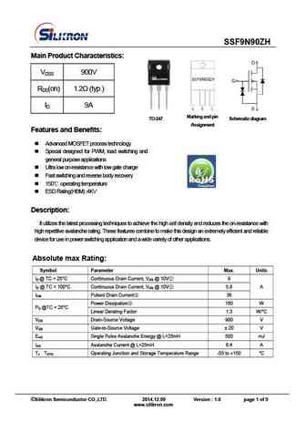
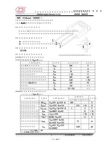
UNISONIC TECHNOLOGIES CO., LTD 9N90 Power MOSFET 9A, 900V N-CHANNEL POWER MOSFET DESCRIPTION The UTC 9N90 uses UTC s advanced proprietary, planar stripe, DMOS technology to provide excellent RDS(ON), low gate charge and operation with low gate voltages. This device is suitable for use as a load switch or in PWM applications. FEATURES * RDS(ON) = 1.4 @VGS = 10 V *
9n90.pdf
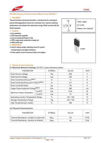
9N90 9A 900V N-channel Enhancement Mode Power MOSFET 1 Description These N-channel enhanced vdmosfets, is obtained by the self-aligned V DSS = 900V planar technology which reduce the conduction loss, improve switching I = 9.0A D performance and enhance the avalanche energy. Which accords with the RoHS standard. R DS(on) TYP) = 920m 2 Features Fast switching ESD impro
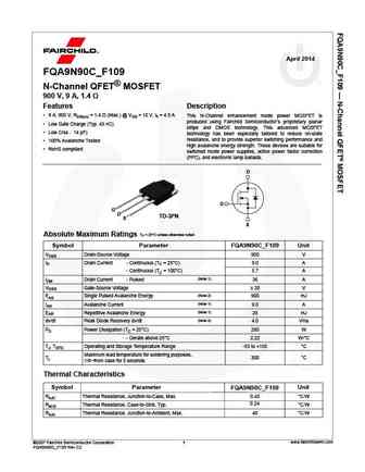
fqa9n90c.pdf
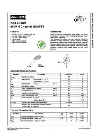
July 2007 QFET FQA9N90C 900V N-Channel MOSFET Features Description 9A, 900V, RDS(on) = 1.4 @VGS = 10 V These N-Channel enhancement mode power field effect Low gate charge ( typical 45 nC) transistors are produced using Fairchild s proprietary, planar stripe, DMOS technology. Low Crss ( typical 14pF) This advanced technology has been especially tailored to Fa
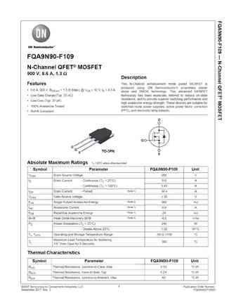
fqa9n90 f109.pdf
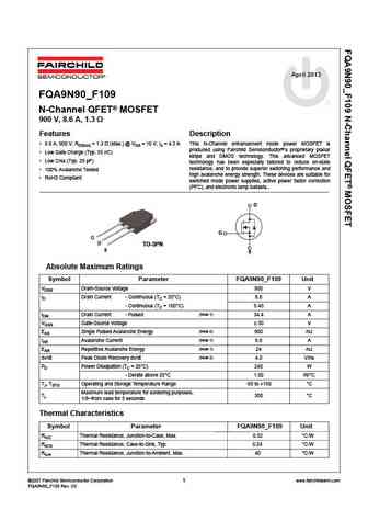
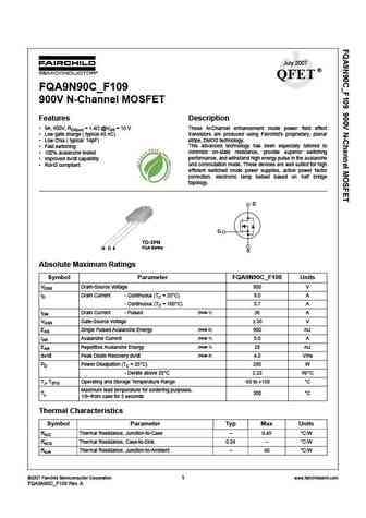
April 2013 FQA9N90_F109 N-Channel QFET MOSFET 900 V, 8.6 A, 1.3 Features Description 8.6 A, 900 V, RDS(on) = 1.3 (Max.) @ VGS = 10 V, ID = 4.3 A This N-Channel enhancement mode power MOSFET is produced using Fairchild Semiconductor s proprietary planar Low Gate Charge (Typ. 55 nC) stripe and DMOS technology. This advanced MOSFET Low Crss (Typ. 25 pF) techn
fqpf9n90ct.pdf

TM QFET FQP9N90C/FQPF9N90C 900V N-Channel MOSFET General Description Features These N-Channel enhancement mode power field effect 8.0 A, 900V, RDS(on) = 1.4 @VGS = 10 V transistors are produced using Fairchild s proprietary, Low gate charge ( typical 45nC) planar stripe, DMOS technology. Low Crss ( typical 14pF) This advanced technology has been especially tailored to
fqp9n90c fqpf9n90c.pdf
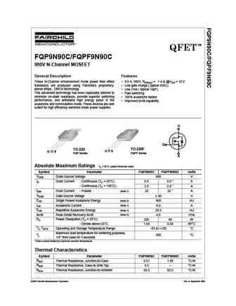
TM QFET FQP9N90C/FQPF9N90C 900V N-Channel MOSFET General Description Features These N-Channel enhancement mode power field effect 8.0 A, 900V, RDS(on) = 1.4 @VGS = 10 V transistors are produced using Fairchild s proprietary, Low gate charge ( typical 45nC) planar stripe, DMOS technology. Low Crss ( typical 14pF) This advanced technology has been especially tailored to
ssh9n90a.pdf
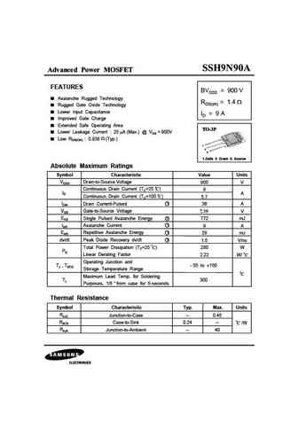
Advanced Power MOSFET FEATURES BVDSS = 900 V Avalanche Rugged Technology RDS(on) = 1.4 Rugged Gate Oxide Technology Lower Input Capacitance ID = 9 A Improved Gate Charge Extended Safe Operating Area Lower Leakage Current 25 A (Max.) @ VDS = 900V Low RDS(ON) 0.938 (Typ.) 1 2 3 1.Gate 2. Drain 3. Source Absolute Maximum Ratings Symbol Characteristic Value Un
ssf9n90a.pdf
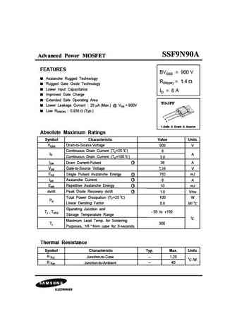
Advanced Power MOSFET FEATURES BVDSS = 900 V Avalanche Rugged Technology RDS(on) = 1.4 Rugged Gate Oxide Technology Lower Input Capacitance ID = 6 A Improved Gate Charge Extended Safe Operating Area Lower Leakage Current 25 A (Max.) @ VDS = 900V Low RDS(ON) 0.938 (Typ.) 1 2 3 1.Gate 2. Drain 3. Source Absolute Maximum Ratings Symbol Characteristic Value
ixfn39n90.pdf
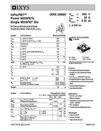
VDSS = 900 V IXFN 39N90 HiPerFETTM ID25 = 39 A Power MOSFETs RDS(on) = 0.22 Single MOSFET Die D trr 250 ns N-Channel Enhancement Mode G Avalanche Rated, High dv/dt, Low t rr S S Symbol Test Conditions Maximum Ratings miniBLOC, SOT-227 B (IXFN) VDSS TJ = 25 C to 150 C 900 V E153432 VDGR TJ = 25 C to 150 C; RGS = 1 M 900
fqa9n90c f109.pdf
April 2014 FQA9N90C_F109 N-Channel QFET MOSFET 900 V, 9 A, 1.4 Features Description 9 A, 900 V, RDS(on) = 1.4 (Max.) @ VGS = 10 V, ID = 4.5 A This N-Channel enhancement mode power MOSFET is produced using Fairchild Semiconductor s proprietary planar Low Gate Charge (Typ. 45 nC) stripe and DMOS technology. This advanced MOSFET Low Crss . 14 pF) technology
fqp9n90c fqpf9n90c.pdf

Is Now Part of To learn more about ON Semiconductor, please visit our website at www.onsemi.com Please note As part of the Fairchild Semiconductor integration, some of the Fairchild orderable part numbers will need to change in order to meet ON Semiconductor s system requirements. Since the ON Semiconductor product management systems do not have the ability to manage part nomenclatur
9n90l-tc3-t 9n90g-tc3-t 9n90l-tf1-t 9n90g-tf1-t 9n90l-tf2-t 9n90g-tf2-t 9n90l-t3p-t 9n90g-t3p-t 9n90l-t3n-t 9n90g-t3n-t 9n90l-t47-t 9n90g-t47-t.pdf
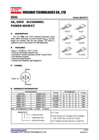
UNISONIC TECHNOLOGIES CO., LTD 9N90 Power MOSFET 9A, 900V N-CHANNEL POWER MOSFET DESCRIPTION The UTC 9N90 uses UTC s advanced proprietary, planar stripe, DMOS technology to provide excellent RDS(ON), low gate charge and operation with low gate voltages. This device is suitable for use as a load switch or in PWM applications. FEATURES * RDS(ON)
9n90l.pdf

UNISONIC TECHNOLOGIES CO., LTD 9N90 Power MOSFET 900V N-CHANNEL MOSFET DESCRIPTION 1 The UTC 9N90 uses UTC s advanced proprietary, planar TO-247 stripe, DMOS technology to provide excellent RDS(ON), low gate charge and operation with low gate voltages. This device is suitable for use as a load switch or in PWM applications. FEATURES * RDS(ON) = 1.4 @VGS = 10 V
fmr09n90e.pdf
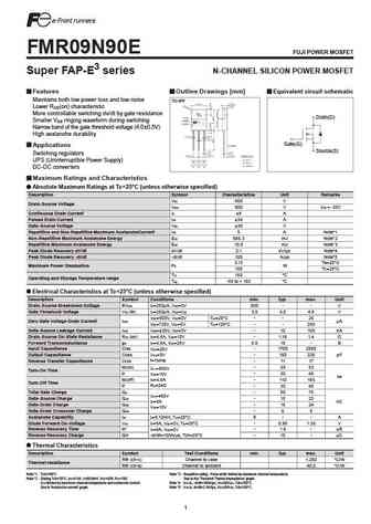
FMR09N90E FUJI POWER MOSFET Super FAP-E3 series N-CHANNEL SILICON POWER MOSFET Features Outline Drawings [mm] Equivalent circuit schematic Maintains both low power loss and low noise TO-3PF Lower R (on) characteristic DS More controllable switching dv/dt by gate resistance Drain(D) Smaller V ringing waveform during switching GS Narrow band of the gate threshold voltage (4.0 0.5V) H
fmh09n90e.pdf
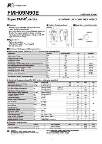
FMH09N90E FUJI POWER MOSFET Super FAP-E3 series N-CHANNEL SILICON POWER MOSFET Features Outline Drawings [mm] Equivalent circuit schematic Maintains both low power loss and low noise TO-3P(Q) Lower R (on) characteristic DS More controllable switching dv/dt by gate resistance Drain(D) Smaller V ringing waveform during switching GS Narrow band of the gate threshold voltage (4.0 0.5V)
fmv09n90e.pdf
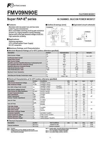
FMV09N90E FUJI POWER MOSFET Super FAP-E3 series N-CHANNEL SILICON POWER MOSFET Features Outline Drawings [mm] Equivalent circuit schematic Maintains both low power loss and low noise TO-220F(SLS) Lower R (on) characteristic DS More controllable switching dv/dt by gate resistance Drain(D) Smaller V ringing waveform during switching GS Narrow band of the gate threshold voltage (4.0 0.
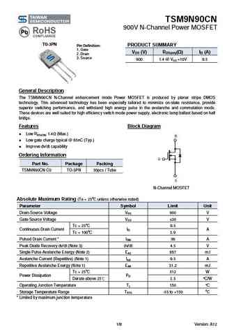
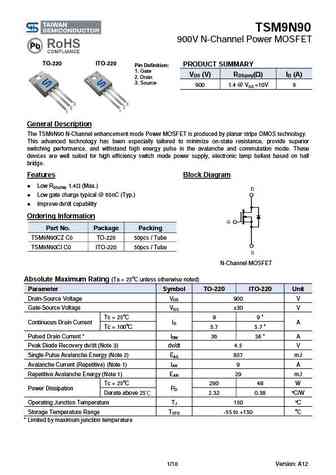
tsm9n90cn.pdf
TSM9N90CN 900V N-Channel Power MOSFET TO-3PN PRODUCT SUMMARY Pin Definition 1. Gate VDS (V) RDS(on)( ) ID (A) 2. Drain 3. Source 900 1.4 @ VGS =10V 9.5 General Description The TSM9N90CN N-Channel enhancement mode Power MOSFET is produced by planar stripe DMOS technology. This advanced technology has been especially tailored to minimize on-state resistance, provide
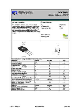
tsm9n90ci tsm9n90cz.pdf
TSM9N90 900V N-Channel Power MOSFET TO-220 ITO-220 PRODUCT SUMMARY Pin Definition 1. Gate VDS (V) RDS(on)( ) ID (A) 2. Drain 3. Source 900 1.4 @ VGS =10V 9 General Description The TSM9N90 N-Channel enhancement mode Power MOSFET is produced by planar stripe DMOS technology. This advanced technology has been especially tailored to minimize on-state resistance, provide
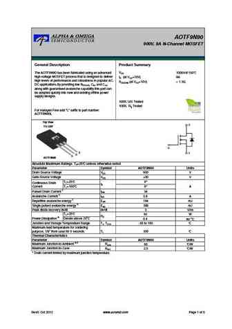
aok9n90.pdf
AOK9N90 900V,9A N-Channel MOSFET General Description Product Summary VDS 1000@150 The AOK9N90 is fabricated using an advanced high voltage MOSFET process that is designed to deliver high ID (at VGS=10V) 9A levels of performance and robustness in popular AC-DC RDS(ON) (at VGS=10V)
aotf9n90.pdf
AOTF9N90 900V, 9A N-Channel MOSFET General Description Product Summary VDS 1000V@150 The AOTF9N90 has been fabricated using an advanced high voltage MOSFET process that is designed to deliver ID (at VGS=10V) 9A high levels of performance and robustness in popular AC- RDS(ON) (at VGS=10V)
ap09n90cw-hf.pdf
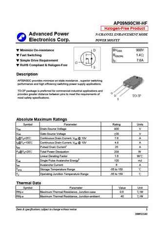
AP09N90CW-HF Halogen-Free Product Advanced Power N-CHANNEL ENHANCEMENT MODE Electronics Corp. POWER MOSFET Minimize On-resistance D BVDSS 900V Fast Switching RDS(ON) 1.4 Simple Drive Requirement ID 7.6A G RoHS Compliant & Halogen-Free S Description AP09N90C provides minimize on-state resistance , superior switching performance and high efficiency switching power su
ap09n90w.pdf
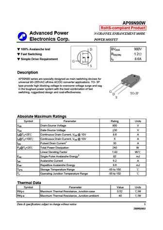
AP09N90W RoHS-compliant Product Advanced Power N-CHANNEL ENHANCEMENT MODE Electronics Corp. POWER MOSFET 100% Avalanche test D BVDSS 900V Fast Switching RDS(ON) 1.2 Simple Drive Requirement ID 8.6A G S Description AP09N90 series are specially designed as main switching devices for universal 90 265VAC off-line AC/DC converter applications. TO- 3P type provide high block
ap09n90cw.pdf
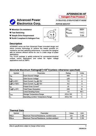
AP09N90CW-HF Halogen-Free Product Advanced Power N-CHANNEL ENHANCEMENT MODE Electronics Corp. POWER MOSFET Minimize On-resistance D BVDSS 900V Fast Switching RDS(ON) 1.4 Simple Drive Requirement ID 7.6A G RoHS Compliant & Halogen-Free S Description AP09N90C series are from Advanced Power innovated design and silicon process technology to achieve the lowest possible
jcs9n90ft jcs9n90wt jcs9n90abt jcs9n90bt.pdf
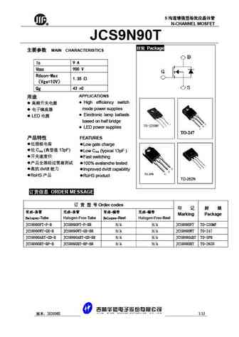
N R N-CHANNEL MOSFET JCS9N90T Package MAIN CHARACTERISTICS ID 9 A VDSS 900 V Rdson-Max 1.35 Vgs=10V Qg 43 nC APPLICATIONS High efficiency switch mode power supplies Electronic lamp ballasts LED based on half bridge LED
jcs9n90ft.pdf
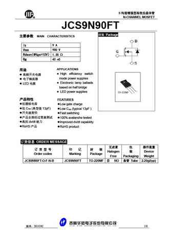
N R N-CHANNEL MOSFET JCS9N90FT Package MAIN CHARACTERISTICS ID 9 A VDSS 900 V Rdson 1.35 @Vgs=10V Qg 43 nC APPLICATIONS High efficiency switch mode power supplies Electronic lamp ballasts LED based on half bridge LED power
9n90b 9n90c.pdf
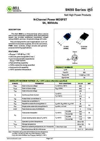
RoHS 9N90 Series RoHS SEMICONDUCTOR Nell High Power Products N-Channel Power MOSFET 9A, 900Volts DESCRIPTION D The Nell 9N90 is a three-terminal silicon device with current conduction capability of 9A, fast switching speed, low on-state resistance, breakdown voltage rating of 900V, and max. threshold voltage of 5 volts. They are designed for use in applications such as G G D
hfh9n90.pdf
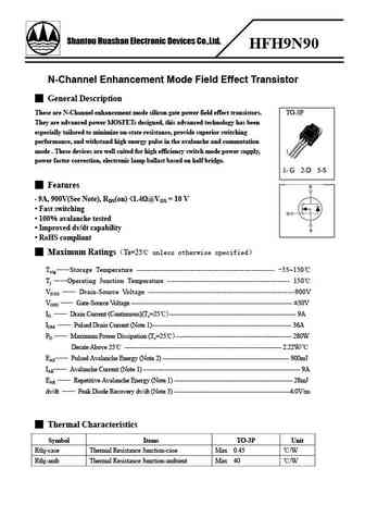
Shantou Huashan Electronic Devices Co.,Ltd. HFH9N90 N-Channel Enhancement Mode Field Effect Transistor General Description These are N-Channel enhancement mode silicon gate power field effect transistors. TO-3P They are advanced power MOSFETs designed, this advanced technology has been especially tailored to minimize on-state resistance, provide superior switching performance
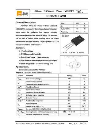
cs9n90f a9d.pdf

Silicon N-Channel Power MOSFET R CS9N90F A9D General Description VDSS 900 V CS9N90F A9HD the silicon N-channel Enhanced ID 9 A PD(TC=25 ) 60 W VDMOSFETs, is obtained by the self-aligned planar Technology RDS(ON)Typ 0.9 which reduce the conduction loss, improve switching performance and enhance the avalanche energy. The transistor can be used in various powe
cs9n90 anhd.pdf
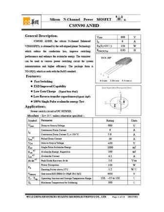
Silicon N-Channel Power MOSFET R CS9N90 ANHD General Description VDSS 900 V CS9N90 ANHD, the silicon N-channel Enhanced ID 9 A PD(TC=25 ) 150 W VDMOSFETs, is obtained by the self-aligned planar Technology RDS(ON)Typ 0.95 which reduce the conduction loss, improve switching performance and enhance the avalanche energy. The transistor can be used in various pow
9n90b.pdf
9N90B 9A 900V N-channel Enhancement Mode Power MOSFET 1 Description These N-channel enhanced vdmosfets, is obtained by the self-aligned V DSS = 900V planar technology which reduce the conduction loss, improve switching I = 9.0A D performance and enhance the avalanche energy. Which accords with the RoHS standard. R DS(on) TYP) = 920m 2 Features Fast switching ESD impr
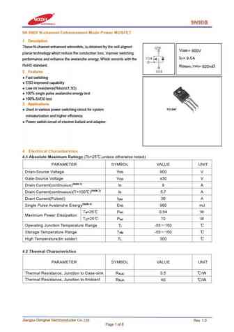
msw9n90.pdf
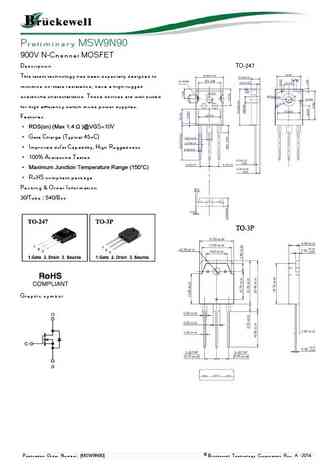
Preliminary MSW9N90 900V N-Channel MOSFET Description TO-247 This latest technology has been especially designed to minimize on-state resistance, have a high rugged avalanche characteristics. These devices are well suited for high efficiency switch mode power supplies. Features RDS(on) (Max 1.4 )@VGS=10V Gate Charge (Typical 45nC) Improved dv/dt Capability, Hi
msf9n90.pdf

MSF9N90 900V N-Channel MOSFET Description The MSF9N90 is a N-channel enhancement-mode MOSFET, providing the designer with the best combination of fast switching, ruggedized device design, low on-resistance and cost effectiveness. The TO-220F package is universally preferred for all commercial-industrial applications Features RDS(on) (Max 1.4 )@VGS=10V Gate Charg
ms9n90.pdf
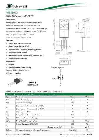
MS9N90 900V N-Channel MOSFET Description The MS9N90 is a N-channel enhancement-mode MOSFET, providing the designer with the best combination of fast switching, ruggedized device design, low on-resistance and cost effectiveness. The TO-220 package is universally preferred for all commercial-industrial applications Features RDS(on) (Max 1.4 )@VGS=10V Gate Charge (
wfw9n90w.pdf
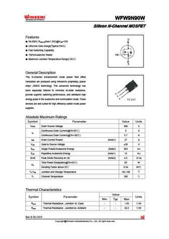
WFW9N90W WFW9N90W WFW9N90W WFW9N90W Silicon N-Channel MOSFET Silicon N-Channel MOSFET Silicon N-Channel MOSFET Silicon N-Channel MOSFET Features 9A,900V, R (Max1.35 )@V =10V DS(on) GS Ultra-low Gate charge(Typical 58nC) Fast Switching Capability 100%Avalanche Tested Maximum Junction Temperature Range(150 ) General Description This N-Channel enhancement mo
wfw9n90.pdf
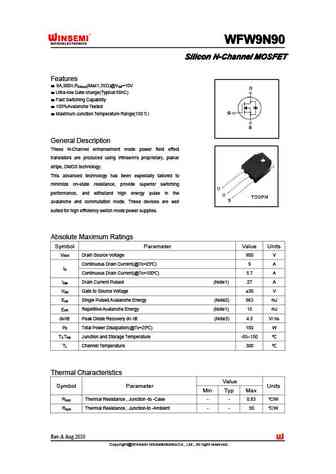
WFW9N90 WFW9N90 WFW9N90 WFW9N90 Silicon N-Channel MOSFET Silicon N-Channel MOSFET Silicon N-Channel MOSFET Silicon N-Channel MOSFET Features 9A,900V,R (Max1.35 )@V =10V DS(on) GS Ultra-low Gate charge(Typical 58nC) Fast Switching Capability 100%Avalanche Tested Maximum Junction Temperature Range(150 ) General Description These N-Channel enhancement mode p
wff9n90.pdf
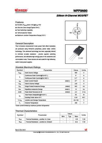
WFF9N90 WFF9N90 WFF9N90 WFF9N90 Silicon N-Channel MOSFET Silicon N-Channel MOSFET Silicon N-Channel MOSFET Silicon N-Channel MOSFET Features 9A,900V, R (Max1.35 )@V =10V DS(on) GS Ultra-low Gate charge(Typical 58nC) Fast Switching Capability 100%Avalanche Tested Maximum Junction Temperature Range(150 ) General Description This N-Channel enhancement mode p
bl9n90-a bl9n90-w bl9n90-f.pdf
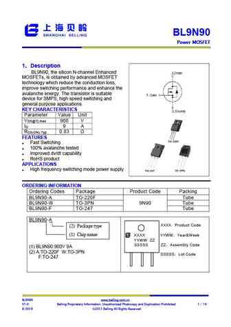
BL9N90 Power MOSFET Power MOSFET Power MOSFET Power MOSFET 1 Description BL9N90, the silicon N-channel Enhanced MOSFETs, is obtained by advanced MOSFET technology which reduce the conduction loss, improve switching performance and enhance the avalanche energy. The transistor is suitable device for SMPS, high speed switching and general purpose applications
jfpc9n90c jffm9n90c.pdf
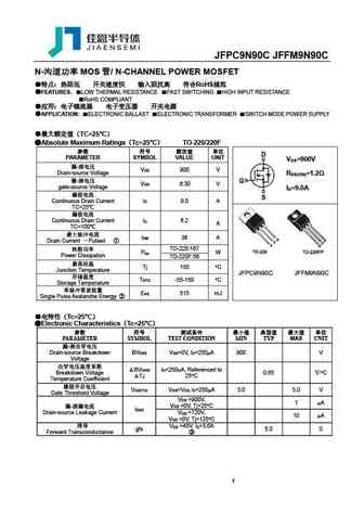
JFPC9N90C JFFM9N90C N- MOS / N-CHANNEL POWER MOSFET RoHS FEATURES LOW THERMAL RESISTANCE FAST SWITCHING HIGH INPUT RESISTANCE RoHS COMPLIANT APPLICATION ELECTRONIC BALLAST ELECTRONIC TRANSFORMER SWITCH MODE POWER SU
slw9n90c.pdf
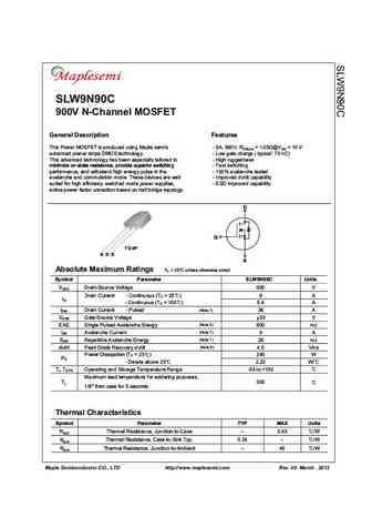
This Power MOSFET is produced using Maple semi s - 9A, 900V, RDS(on) = 1.05 @VGS = 10 V advanced planar stripe DMOS technology. - Low gate charge ( typical 70 nC) This advanced technology has been especially tailored to - High ruggedness minimize on-state resistance, provide superior switching Fast switching minimize on state r
ptw09n90.pdf
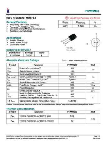
PTW09N90 900V N-Channel MOSFET General Features BVDSS RDS(ON),typ. ID Proprietary New Planar Technology 900V 1.12 9A RDS(ON),typ.=1.12 @VGS=10V Low Gate Charge Minimize Switching Loss Fast Recovery Body Diode Applications Adaptor Charger SMPS Power Supply LCD Panel Power Ordering Information Part Number Package Brand PTW09N90 TO-3P Absolute Maximum Rat
ptp09n90 pta09n90.pdf
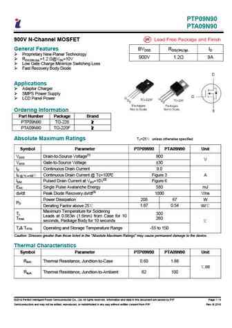
PTP09N90 PTA09N90 900V N-Channel MOSFET General Features BVDSS RDS(ON),typ. ID Proprietary New Planar Technology 900V 1.2 9A RDS(ON),typ.=1.2 @VGS=10V Low Gate Charge Minimize Switching Loss Fast Recovery Body Diode Applications Adaptor Charger SMPS Power Supply LCD Panel Power Ordering Information Part Number Package Brand PTP09N90 TO-220 PTA09N90
hfs9n90a.pdf
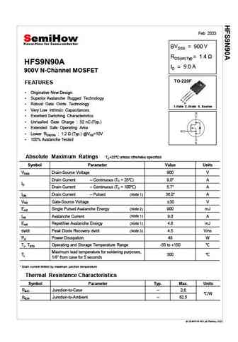
Feb 2023 BVDSS = 900 V RDS(on) Typ = 1.4 HFS9N90A ID = 9.0 A 900V N-Channel MOSFET TO-220F FEATURES Originative New Design Superior Avalanche Rugged Technology 1 2 3 Robust Gate Oxide Technology 1.Gate 2. Drain 3. Source Very Low Intrinsic Capacitances Excellent Switching Characteristics Unrivalled Gate Charge 52 nC (Typ.) Extended Safe Operat
hfa9n90.pdf
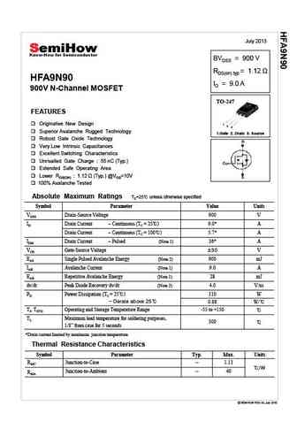
July 2013 BVDSS = 900 V RDS(on) typ HFA9N90 ID = 9.0 A 900V N-Channel MOSFET TO-247 FEATURES Originative New Design 1 2 3 Superior Avalanche Rugged Technology 1.Gate 2. Drain 3. Source Robust Gate Oxide Technology Very Low Intrinsic Capacitances Excellent Switching Characteristics Unrivalled Gate Charge 55 nC (Typ.) Extended Safe Operating Area Low
ssm09n90gw.pdf
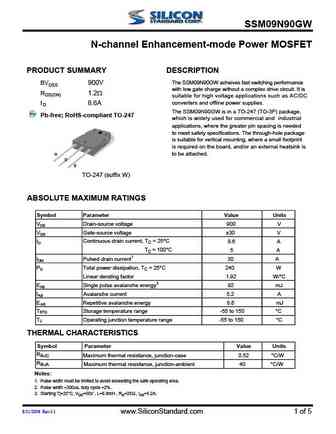
SSM09N90GW N-channel Enhancement-mode Power MOSFET PRODUCT SUMMARY DESCRIPTION The SSM09N90GW acheives fast switching performance BVDSS 900V with low gate charge without a complex drive circuit. It is RDS(ON) 1.2 suitable for high voltage applications such as AC/DC converters and offline power supplies. I 8.6A D The SSM09N90GW is in a TO-247 (TO-3P) package, Pb-free; RoHS-compli
ssm09n90cgw.pdf
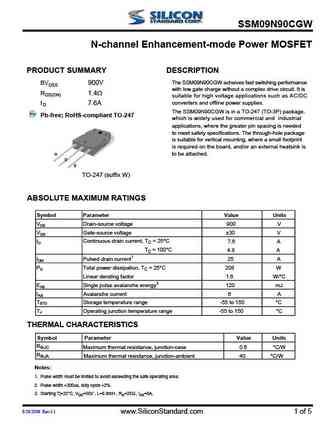
SSM09N90CGW N-channel Enhancement-mode Power MOSFET PRODUCT SUMMARY DESCRIPTION The SSM09N90CGW acheives fast switching performance BVDSS 900V with low gate charge without a complex drive circuit. It is RDS(ON) 1.4 suitable for high voltage applications such as AC/DC converters and offline power supplies. I 7.6A D The SSM09N90CGW is in a TO-247 (TO-3P) package, Pb-free; RoHS-com
msu9n90p.pdf
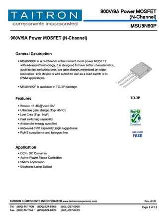
900V/9A Power MOSFET (N-Channel) MSU9N90P 900V/9A Power MOSFET (N-Channel) General Description MSU9N90P is a N-Channel enhancement mode power MOSFET with advanced technology. It is designed to have better characteristics, such as fast switching time, low gate charge, minimized on-state resistance. This device is well suited for use as a load switch or in PWM applications.
tmp9n90 tmpf9n90.pdf
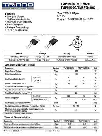
TMP9N90/TMPF9N90 TMP9N90G/TMPF9N90G VDSS = 990 V @Tjmax Features ID = 9A Low gate charge RDS(ON) = 1.4 W(max) @ VGS= 10 V 100% avalanche tested Improved dv/dt capability RoHS compliant Halogen free package JEDEC Qualification D G S Device Package Marking Remark TMP9N90 / TMPF9N90 TO-220 / TO-220F TMP9N90 / TMPF9N90 RoHS TMP9N90G / TMPF9N
tman9n90.pdf
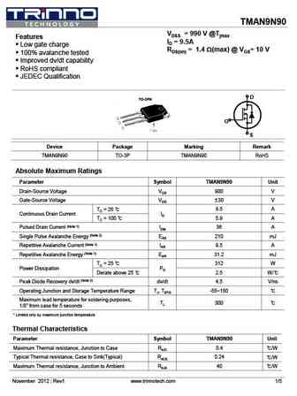
TMAN9N90 VDSS = 990 V @Tjmax Features ID = 9.5A Low gate charge RDS(on) = 1.4 W(max) @ VGS= 10 V 100% avalanche tested Improved dv/dt capability RoHS compliant JEDEC Qualification D TO-3PN G S Device Package Marking Remark TMAN9N90 TO-3P TMAN9N90 RoHS Absolute Maximum Ratings Parameter Symbol TMAN9N90 Unit Drain-Source Voltage VDS 900 V
tman9n90az.pdf
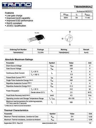
TMAN9N90AZ N-channel MOSFET Features BVDSS ID RDS(on) Low gate charge 900V 9A
tsa9n90m.pdf
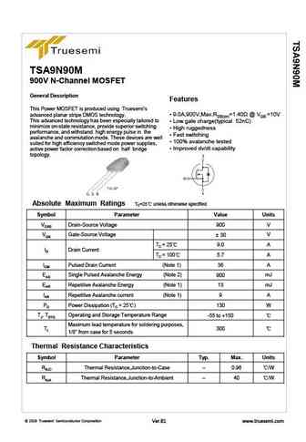
TSA9N90M 900V N-Channel MOSFET General Description Features This Power MOSFET is produced using Truesemi s 9.0A,900V,Max.RDS(on)=1.40 @ VGS =10V advanced planar stripe DMOS technology. This advanced technology has been especially tailored to Low gate charge(typical 52nC) minimize on-state resistance, provide superior switching High ruggedness performance, and
tsf9n90m.pdf
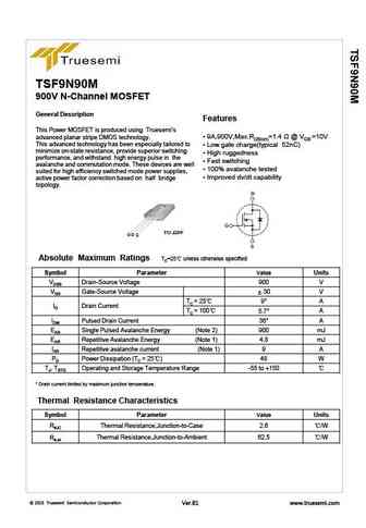
TSF9N90M 900V N-Channel MOSFET General Description Features This Power MOSFET is produced using Truesemi s 9A,900V,Max.RDS(on)=1.4 @ VGS =10V advanced planar stripe DMOS technology. This advanced technology has been especially tailored to Low gate charge(typical 52nC) minimize on-state resistance, provide superior switching High ruggedness performance, and
wmj9n90d1b wml9n90d1b.pdf
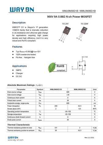
WMJ9N90D1B WML9N90D1B 900V 9A 0.88 N-ch Power MOSFET Description TO-247 TO-220F WMOSTM D1 is Wayon s 1st generation VDMOS family that is dramatic reduction in on-resistance and ultra-low gate charge for applications requiring high power density and high efficiency. And it is very G D G S D robust and RoHS compliant. S Features Typ.R =0.88 @V =10V DS(on) GS 100% av
cs9n90anhd.pdf

Silicon N-Channel Power MOSFET R CS9N90 ANHD General Description VDSS 900 V CS9N90 ANHD, the silicon N-channel Enhanced ID 9 A PD(TC=25 ) 150 W VDMOSFETs, is obtained by the self-aligned planar Technology RDS(ON)Typ 0.95 which reduce the conduction loss, improve switching performance and enhance the avalanche energy. The transistor can be used in various pow
cs9n90fa9d.pdf
Silicon N-Channel Power MOSFET R CS9N90F A9D General Description VDSS 900 V CS9N90F A9HD the silicon N-channel Enhanced ID 9 A PD(TC=25 ) 60 W VDMOSFETs, is obtained by the self-aligned planar Technology RDS(ON)Typ 0.9 which reduce the conduction loss, improve switching performance and enhance the avalanche energy. The transistor can be used in various powe
cs9n90f cs9n90p cs9n90w cs9n90v.pdf
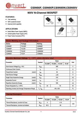
nvert Suzhou Convert Semiconductor Co ., Ltd. CS9N90F, CS9N90P,CS9N90W,CS9N90V 900V N-Channel MOSFET FEATURES Fast switching 100% avalanche tested Improved dv/dt capability APPLICATIONS Switch Mode Power Supply (SMPS) Uninterruptible Power Supply (UPS) Power Factor Correction (PFC) Device Marking and Package Information Device Package Marking CS9N90F TO-220
fir9n90fg.pdf
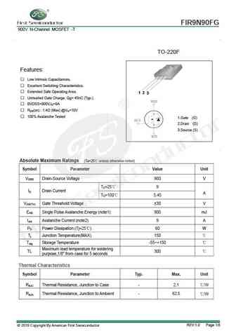
FIR9N90FG 900V N-Channel MOSFET -T TO-220F Features Low Intrinsic Capacitances. Excellent Switching Characteristics. Extended Safe Operating Area. Unrivalled Gate Charge Qg= 45nC (Typ.). BVDSS=900V,ID=9A RDS(on) 1.4 (Max) @VG=10V 100% Avalanche Tested 1.Gate (G) 2.Drain (D) 3.Source (S) Absolute Maximum Ratings (Ta=25 unless otherwise noted)
ha9n90.pdf
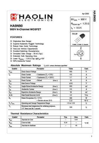
Apr 2009 BVDSS = 900 V RDS(on) typ 5 HA9N90 ID = 9.0 A 900V N-Channel MOSFET TO-3P FEATURES 1 Originative New Design 2 3 Superior Avalanche Rugged Technology 1.Gate 2. Drain 3. Source Robust Gate Oxide Technology Very Low Intrinsic Capacitances Excellent Switching Characteristics Unrivalled Gate Charge 55 nC (Typ.) Extended Safe Operating Area Lower RDS(ON)
hm9n90f.pdf
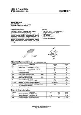
HM9N90 HM9N90 900V N-Channel MOSFET General Description Features This Power MOSFET is produced using SL semi s 9.0A, 900V, RDS(on) = 1.40 @VGS = 10 V advanced planar stripe DMOS technology. Low gate charge ( typical 45nC) This advanced technology has been espe cially tailored to High ruggedness minimize o n-state r esistance, pr ovide superior switching Fast wit
sfp049n90c3 sfb046n90c3.pdf
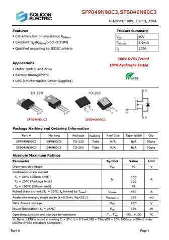
SFP049N90C3,SFB046N90C3 N-MOSFET 90V, 3.9m , 120A Features Product Summary Extremely low on-resistance RDS(on) VDS 90V Excellent QgxRDS(on) product(FOM) RDS(on) 3.9m Qualified according to JEDEC criteria ID 120A 100% DVDS Tested Applications 100% Avalanche Tested Motor control and drive Battery management UPS (Uninterrupible Power Supplies) SFP049N90
md9n90.pdf
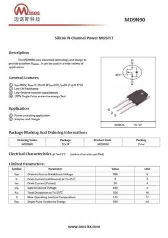
Silicon N-Channel Power MOSFET Description The MD9N90 uses advanced technology and design to provide excellent R . It can be used in a wide variety of DS(ON) applications. General Features V =900V, R
fxn9n90p.pdf
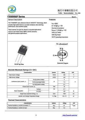
FuXin Semiconductor Co., Ltd. FXN9N90P Series Rev.A General Description Features The FXN9N90P uses advanced Silicon s MOSFET Technology, which V = 900V DS provides high performance in on-state resistance, fast switching ID = 9A @V = 10V GS performance, and excellent quality. Very low on-resistance These devices can also be utilized in indus
fxn9n90f.pdf
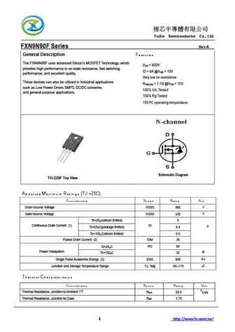
FuXin Semiconductor Co., Ltd. FXN9N90F Series Rev.A General Description Features The FXN9N90F uses advanced Silicon s MOSFET Technology, which V = 900V DS provides high performance in on-state resistance, fast switching ID = 9A @V = 10V GS performance, and excellent quality. Very low on-resistance These devices can also be utilized in indus
fmr09n90e.pdf
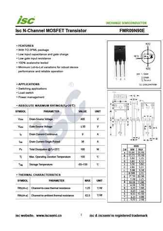
INCHANGE Semiconductor Isc N-Channel MOSFET Transistor FMR09N90E FEATURES With TO-3PML package Low input capacitance and gate charge Low gate input resistance 100% avalanche tested Minimum Lot-to-Lot variations for robust device performance and reliable operation APPLICATIONS Switching applications Load switch Power management ABSOLUTE MAXIMUM RATINGS(T =25
fqpf9n90c.pdf
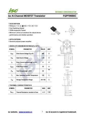
isc N-Channel MOSFET Transistor FQPF9N90C DESCRIPTION RDS(on) = 1.4 @VGS = 10 V, ID = 4 A Fast Switching Speed 100% Avalanche Tested Minimum Lot-to-Lot variations for robust device performance and reliable operation APPLICATIONS General purpose power amplifier ABSOLUTE MAXIMUM RATINGS(T =25 ) C SYMBOL PARAMETER VALUE UNIT V Drain-Source Voltage (V =0) 900 V DS
aok9n90.pdf
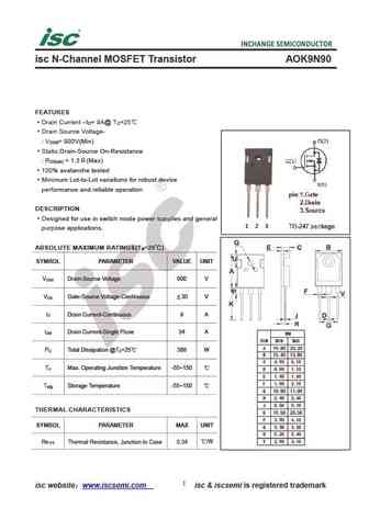
isc N-Channel MOSFET Transistor AOK9N90 FEATURES Drain Current I = 9A@ T =25 D C Drain Source Voltage- V = 900V(Min) DSS Static Drain-Source On-Resistance R = 1.3 (Max) DS(on) 100% avalanche tested Minimum Lot-to-Lot variations for robust device performance and reliable operation DESCRIPTION Designed for use in switch mode power supplies and general purpose
aotf9n90.pdf
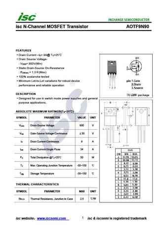
isc N-Channel MOSFET Transistor AOTF9N90 FEATURES Drain Current I = 9A@ T =25 D C Drain Source Voltage- V = 900V(Min) DSS Static Drain-Source On-Resistance R = 1.3 (Max) DS(on) 100% avalanche tested Minimum Lot-to-Lot variations for robust device performance and reliable operation DESCRIPTION Designed for use in switch mode power supplies and general purpos
fmh09n90e.pdf
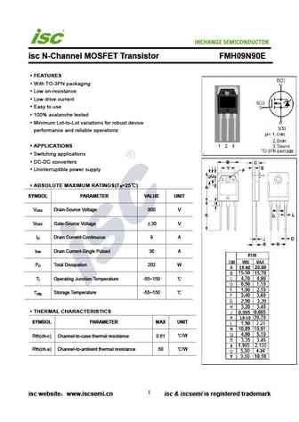
INCHANGE Semiconductor isc N-Channel MOSFET Transistor FMH09N90E FEATURES With TO-3PN packaging Low on-resistance Low drive current Easy to use 100% avalanche tested Minimum Lot-to-Lot variations for robust device performance and reliable operationz APPLICATIONS Switching applications DC-DC converters Uninterruptible power supply ABSOLUTE MAXIMUM RATINGS(T
9n90l.pdf
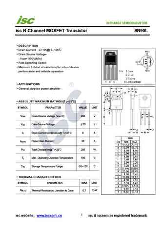
isc N-Channel MOSFET Transistor 9N90L DESCRIPTION Drain Current I = 9A@ T =25 D C Drain Source Voltage- V = 900V(Min) DSS Fast Switching Speed Minimum Lot-to-Lot variations for robust device performance and reliable operation APPLICATIONS General purpose power amplifier ABSOLUTE MAXIMUM RATINGS(T =25 ) C SYMBOL PARAMETER VALUE UNIT V Drain-Source Voltage (V
ap9n90f ap9n90p ap9n90t.pdf

AP9N90FIPIT 900V N-Channel Enhancement Mode MOSFET Description The AP9N90F/T/P is silicon N-channel Enhanced VDMOSFETs, is obtained by the self-aligned planar Technology which reduce the conduction loss, improve switching performance and enhance the avalanche energy. The transistor can be used in various power switching circuit for system miniaturization and higher efficiency.
Otros transistores... STK003SF, STK004SF, SUF1002, SUF2001, SUF3001, SUM201MN, SUM202MN, 8N90, IRLZ44N, 10N90, 11N90, 12N90, 9N95, 9N100, 1N90, 2N90, 3N90
Parámetros del MOSFET. Cómo se afectan entre sí.
History: 25N40
🌐 : EN ES РУ

Liste
Recientemente añadidas las descripciónes de los transistores:
MOSFET: MSQ60P04D | MSQ40P07D | MSQ30P40D | MSQ30P15 | MSQ30P07D | MSQ100N03D | MSHM60P14 | MSHM40N085 | MSHM30N46 | MSH60N35D | MSH40N032 | MSH30P100 | MSH100N045SA | MSD60P16 | MSD40P45 | MSB100N023
Popular searches
irf530 datasheet | 2sc2625 | 2sc1815 transistor | 2sd718 | 2n3053 transistor | 2sc458 replacement | bc557 transistor | 2n3638