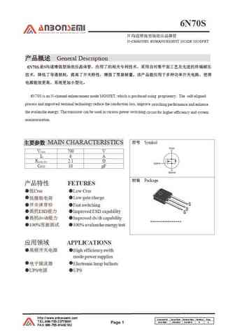
6N70 MOSFET Equivalente. Reemplazo. Hoja de especificaciones. Principales características
Número de Parte: 6N70
Tipo de FET: MOSFET
Polaridad de transistor: N
ESPECIFICACIONES MÁXIMAS
Pdⓘ - Máxima disipación de potencia: 125 W
|Vds|ⓘ - Voltaje máximo drenador-fuente: 700 V
|Vgs|ⓘ - Voltaje máximo fuente-puerta: 30 V
|Id|ⓘ - Corriente continua de drenaje: 6 A
Tjⓘ - Temperatura máxima de unión: 150 °C
CARACTERÍSTICAS ELÉCTRICAS
trⓘ - Tiempo de subida: 48 nS
Cossⓘ - Capacitancia de salida: 90 pF
RDSonⓘ - Resistencia estado encendido drenaje a fuente: 1.6 Ohm
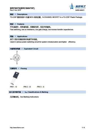
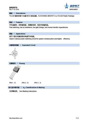
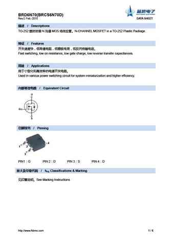
Encapsulados: TO-263 TO-220F TO-220
Búsqueda de reemplazo de 6N70 MOSFET
- Selecciónⓘ de transistores por parámetros
6N70 datasheet
6n70.pdf
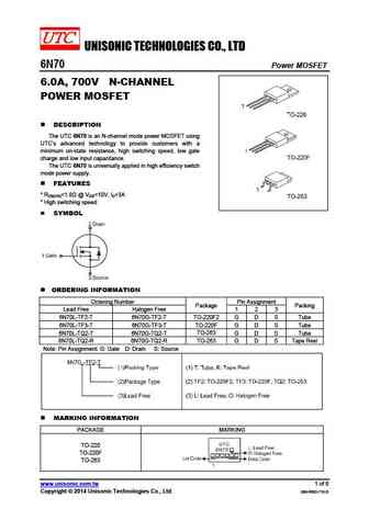
UNISONIC TECHNOLOGIES CO., LTD 6N70 Power MOSFET 6.0A, 700V N-CHANNEL POWER MOSFET DESCRIPTION The UTC 6N70 is an N-channel mode power MOSFET using UTC s advanced technology to provide customers with a minimum on-state resistance, high switching speed, low gate charge and low input capacitance. The UTC 6N70 is universally applied in high efficiency switch mode power sup
6n70 6n70f.pdf
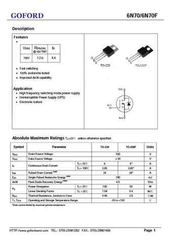
6N70/6N70F GOFORD Description Features VDSS RDS(ON) ID @ 10V (typ) 6 A 700V 1.2 Fast switching 100% avalanche tested Improved dv/dt capability Application High frequency switching mode power supply Uninterruptible Power Supply (UPS) Electronic ballast Absolute Maximum Ratings TC=25 unless otherwise specified Symbol Parameter TO-22
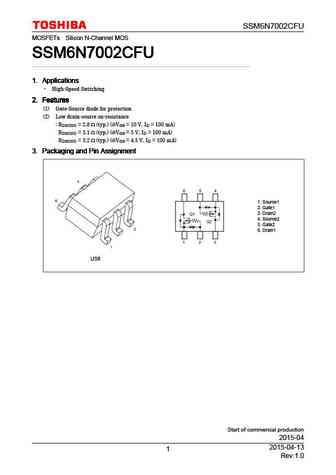
ssm6n7002cfu.pdf
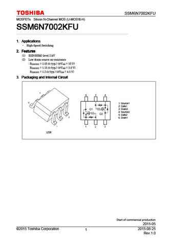
SSM6N7002CFU MOSFETs Silicon N-Channel MOS SSM6N7002CFU SSM6N7002CFU SSM6N7002CFU SSM6N7002CFU 1. Applications 1. Applications 1. Applications 1. Applications High-Speed Switching 2. Features 2. Features 2. Features 2. Features (1) Gate-Source diode for protection (2) Low drain-source on-resistance RDS(ON) = 2.8 (typ.) (@VGS = 10 V, ID = 100 mA) RDS(ON) = 3.1 (t
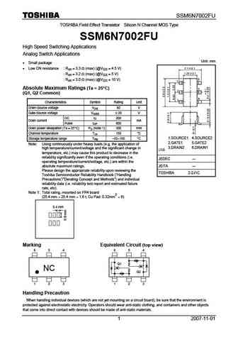
ssm6n7002fu.pdf
SSM6N7002FU TOSHIBA Field Effect Transistor Silicon N Channel MOS Type SSM6N7002FU High Speed Switching Applications Analog Switch Applications Unit mm Small package Low ON resistance Ron = 3.3 (max) (@VGS = 4.5 V) Ron = 3.2 (max) (@VGS = 5 V) Ron = 3.0 (max) (@VGS = 10 V) Absolute Maximum Ratings (Ta = 25 C) (Q1, Q2 Common) Characteristics Symbol
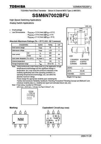
ssm6n7002bfu.pdf
SSM6N7002BFU TOSHIBA Field-Effect Transistor Silicon N Channel MOS Type (U-MOS ) SSM6N7002BFU High-Speed Switching Applications Analog Switch Applications Unit mm 2.1 0.1 Small package 1.25 0.1 Low ON-resistance RDS(ON) = 3.3 (max) (@VGS = 4.5 V) RDS(ON) = 2.6 (max) (@VGS = 5 V) 1 6 RDS(ON) = 2.1 (max) (@VGS = 10 V) 2 5 Absolute Maximum Ratings
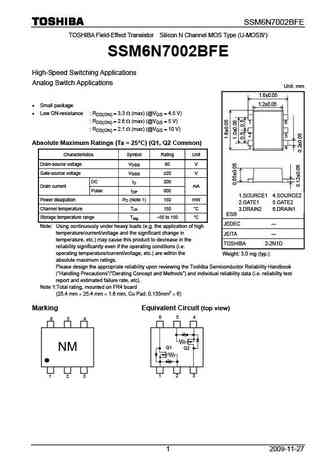
ssm6n7002bfe.pdf
SSM6N7002BFE TOSHIBA Field-Effect Transistor Silicon N Channel MOS Type (U-MOS ) SSM6N7002BFE High-Speed Switching Applications Analog Switch Applications Unit mm 1.6 0.05 1.2 0.05 Small package Low ON-resistance RDS(ON) = 3.3 (max) (@VGS = 4.5 V) RDS(ON) = 2.6 (max) (@VGS = 5 V) 1 6 RDS(ON) = 2.1 (max) (@VGS = 10 V) 2 5 Absolute Maximum Rating
ssm6n7002kfu.pdf
SSM6N7002KFU MOSFETs Silicon N-Channel MOS (U-MOS -H) SSM6N7002KFU SSM6N7002KFU SSM6N7002KFU SSM6N7002KFU 1. Applications 1. Applications 1. Applications 1. Applications High-Speed Switching 2. Features 2. Features 2. Features 2. Features (1) ESD(HBM) level 2 kV (2) Low drain-source on-resistance RDS(ON) = 1.05 (typ.) (@VGS = 10 V) RDS(ON) = 1.15 (typ.) (@VGS
fqp6n70.pdf
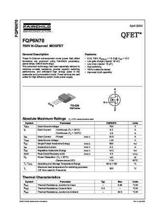
April 2000 TM QFET QFET QFET QFET 700V N-ChanneI MOSFET GeneraI Description Features These N-Channel enhancement mode power field effect 6.2A, 700V, RDS(on) = 1.5 @ VGS = 10 V transistors are produced using Fairchild s proprietary, Low gate charge ( typical 30 nC) planar stripe, DMOS technology. Low Crss ( typical 15 pF) This advanced technology has bee
fqpf6n70.pdf
December 2000 TM QFET QFET QFET QFET FQPF6N70 700V N-Channel MOSFET General Description Features These N-Channel enhancement mode power field effect 3.5A, 700V, RDS(on) = 1.5 @ VGS = 10 V transistors are produced using Fairchild s proprietary, Low gate charge ( typical 30 nC) planar stripe, DMOS technology. Low Crss ( typical 15 pF) This advanced technology is esp
fqa6n70.pdf
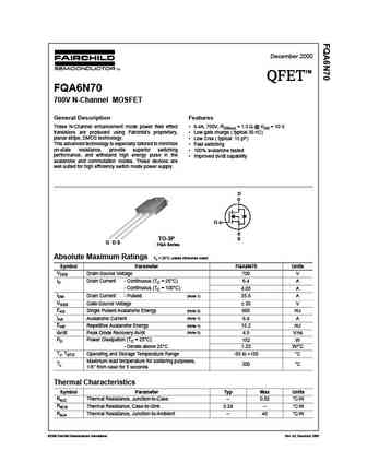
December 2000 TM QFET QFET QFET QFET FQA6N70 700V N-Channel MOSFET General Description Features These N-Channel enhancement mode power field effect 6.4A, 700V, RDS(on) = 1.5 @ VGS = 10 V transistors are produced using Fairchild s proprietary, Low gate charge ( typical 30 nC) planar stripe, DMOS technology. Low Crss ( typical 15 pF) This advanced technology is espe
fqb6n70tm.pdf
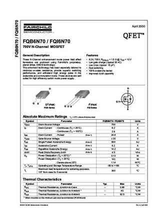
April 2000 TM QFET QFET QFET QFET FQB6N70 / FQI6N70 700V N-ChanneI MOSFET GeneraI Description Features These N-Channel enhancement mode power field effect 6.2A, 700V, RDS(on) = 1.5 @ VGS = 10 V transistors are produced using Fairchild s proprietary, Low gate charge ( typical 30 nC) planar stripe, DMOS technology. Low Crss ( typical 15 pF) This advanced technolog
ssp6n70a.pdf
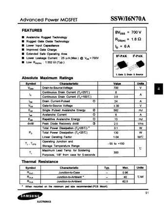
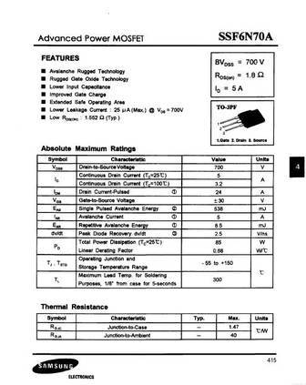
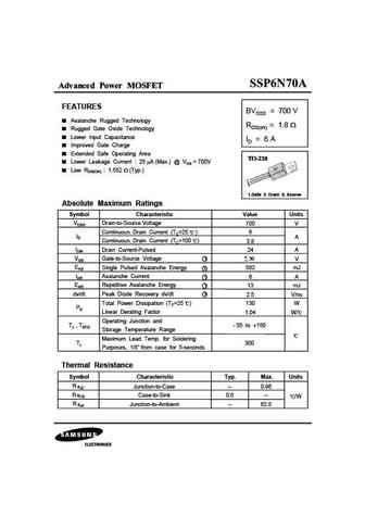
Advanced Power MOSFET FEATURES BVDSS = 700 V Avalanche Rugged Technology RDS(on) = 1.8 Rugged Gate Oxide Technology Lower Input Capacitance ID = 6 A Improved Gate Charge Extended Safe Operating Area Lower Leakage Current 25 A (Max.) @ VDS = 700V Low RDS(ON) 1.552 (Typ.) 1 2 3 1.Gate 2. Drain 3. Source Absolute Maximum Ratings Symbol Characteristic Value
sss6n70a.pdf
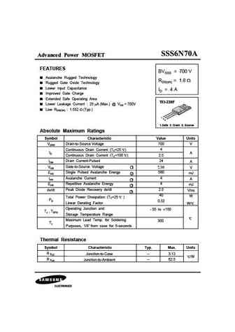
Advanced Power MOSFET FEATURES BVDSS = 700 V Avalanche Rugged Technology RDS(on) = 1.8 Rugged Gate Oxide Technology Lower Input Capacitance ID = 4 A Improved Gate Charge Extended Safe Operating Area Lower Leakage Current 25 A (Max.) @ VDS = 700V Low RDS(ON) 1.552 (Typ.) 1 2 3 1.Gate 2. Drain 3. Source Absolute Maximum Ratings Symbol Characteristic Value
ssh6n70a.pdf
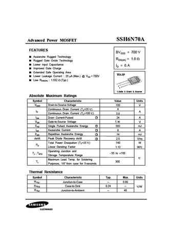
Advanced Power MOSFET FEATURES BVDSS = 700 V Avalanche Rugged Technology RDS(on) = 1.8 Rugged Gate Oxide Technology Lower Input Capacitance ID = 6 A Improved Gate Charge Extended Safe Operating Area Lower Leakage Current 25 A (Max.) @ VDS = 700V Low RDS(ON) 1.552 (Typ.) 1 2 3 1.Gate 2. Drain 3. Source Absolute Maximum Ratings Symbol Characteristic Value
6n70kl-tf3-t 6n70kg-tf3-t 6n70kl-tf1-t 6n70kg-tf1-t 6n70kl-tf2-t 6n70kg-tf2-t 6n70kl-tf3t-t 6n70kg-tf3t-t 6n70kl-tm3-t 6n70kg-tm3-t.pdf
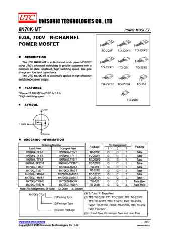
UNISONIC TECHNOLOGIES CO., LTD 6N70K-MT Power MOSFET 6.0A, 700V N-CHANNEL POWER MOSFET DESCRIPTION The UTC 6N70K-MT is an N-channel mode power MOSFET using UTC s advanced technology to provide customers with a minimum on-state resistance, high switching speed, low gate charge and low input capacitance. The UTC 6N70K-MT is universally applied in high efficiency switch m
6n70kl-tms-t 6n70kg-tms-t 6n70kl-tms2-t 6n70kg-tms2-t 6n70kl-tms4-t 6n70kg-tms4-t 6n70kl-tn3-r 6n70kg-tn3-r 6n70kl-tnd-r 6n70kg-tnd-r.pdf
UNISONIC TECHNOLOGIES CO., LTD 6N70K-MT Power MOSFET 6.0A, 700V N-CHANNEL POWER MOSFET DESCRIPTION The UTC 6N70K-MT is an N-channel mode power MOSFET using UTC s advanced technology to provide customers with a minimum on-state resistance, high switching speed, low gate charge and low input capacitance. The UTC 6N70K-MT is universally applied in high efficiency switch m
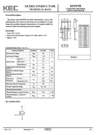
kf6n70i.pdf
KF6N70I SEMICONDUCTOR N CHANNEL MOS FIELD TECHNICAL DATA EFFECT TRANSISTOR General Description A H This planar stripe MOSFET has better characteristics, such as fast C J switching time, fast reverse recovery time, low on resistance, low gate charge and excellent avalanche characteristics. It is mainly suitable for DIM MILLIMETERS electronic ballast and switching mode power supplie
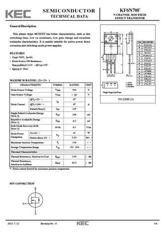
kf6n70f.pdf
KF6N70F SEMICONDUCTOR N CHANNEL MOS FIELD TECHNICAL DATA EFFECT TRANSISTOR General Description C A This planar stripe MOSFET has better characteristics, such as fast switching time, low on resistance, low gate charge and excellent avalanche characteristics. It is mainly suitable for active power factor E DIM MILLIMETERS _ A 10.16 0.2 + correction and switching mode power supplie
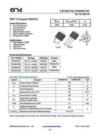
ftu06n70c ftd06n70c.pdf
FTU06N70C/FTD06N70C Doc. NO QRD-310 700V N-Channel MOSFET BVDSS RDS(ON) (Max.) ID General Features 700V 1.8 6.0A Low ON Resistance Low Gate Charge Fast Switching 100% Avalanche Tested D RoHS Compliant/Lead Free Halogen-free available Applications G G High Efficiency SMPS D S G S Adaptor/Charger D S Active PFC To-252
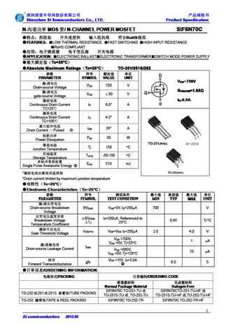
sif6n70c.pdf
Shenzhen SI Semiconductors Co., LTD. Product Specification Shenzhen SI Semiconductors Co., LTD. Product Specification Shenzhen SI Semiconductors Co., LTD. Product Specification Shenzhen SI Semiconductors Co., LTD. Product Specification N- MOS / N-CHANNEL POWER MOSFET SIF6N70C N- MOS / N-CHANNEL POWER MOSFET SIF6N70C N- MOS / N-CHANN
jcs6n70f.pdf
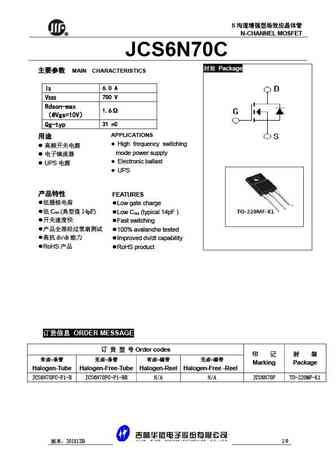
N R N-CHANNEL MOSFET JCS6N70C Package MAIN CHARACTERISTICS ID 6.0 A VDSS 700 V Rdson-max 1.6 @Vgs=10V Qg-typ 31 nC APPLICATIONS High frequency switching mode power supply Electronic ballast UPS UPS FEATUR
jcs6n70vc.pdf
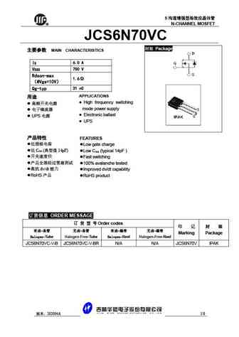
N R N-CHANNEL MOSFET JCS6N70VC Package MAIN CHARACTERISTICS ID 6.0 A VDSS 700 V Rdson-max 1.6 @Vgs=10V Qg-typ 31 nC APPLICATIONS High frequency switching mode power supply Electronic ballast UPS UPS FEATU
jcs6n70v jcs6n70mp jcs6n70b jcs6n70s jcs6n70c jcs6n70f jcs6n70b jcs6n70r.pdf
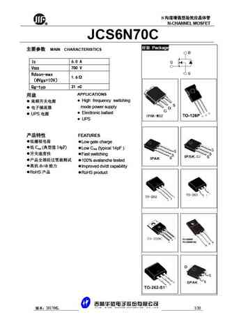
N R N-CHANNEL MOSFET JCS6N70C Package MAIN CHARACTERISTICS ID 6.0 A VDSS 700 V Rdson-max 1.6 @Vgs=10V Qg-typ 31 nC APPLICATIONS High frequency switching mode power supply Electronic ballast UPS UPS FEATUR
mtn6n70fp.pdf
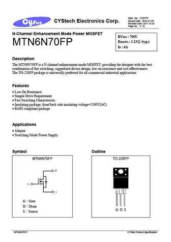
Spec. No. C597FP Issued Date 2010.01.28 CYStech Electronics Corp. Revised Date 2011.10.24 Page No. 1/ 10 N-Channel Enhancement Mode Power MOSFET BVDSS 700V RDS(ON) 1.23 (typ.) MTN6N70FP ID 6A Description The MTN6N70FP is a N-channel enhancement-mode MOSFET, providing the designer with the best combination of fast switching, ruggedized device design, low on-
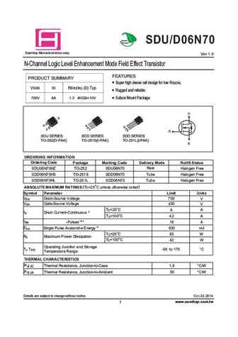
sdu06n70 sdd06n70.pdf
Green Product SDU/D06N70 SamHop Microelectronics corp. Ver 1.0 N-Channel Logic Level Enhancement Mode Field Effect Transistor FEATURES PRODUCT SUMMARY Super high dense cell design for low RDS(ON). VDSS ID RDS(ON) ( ) Typ Rugged and reliable. 700V 6A 1.3 @VGS=10V Suface Mount Package. D G G S S SDU SERIES SDD SERIES SDD SERIES TO-252(D-PAK) TO-251S(I-PAK) TO-251L(I-PAK) ORDERI
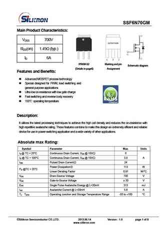
ssf6n70gm.pdf
SSF6N70GM Main Product Characteristics VDSS 700V RDS(on) 1.49 (typ.) ID 6A IPAKM-S2 Marking and p in S che ma ti c di ag ra m (Details in page6) Assignment Features and Benefits Advanced MOSFET process technology Special designed for PWM, load switching and general purpose applications Ultra low on-resistance with low gate charge Fast switching and
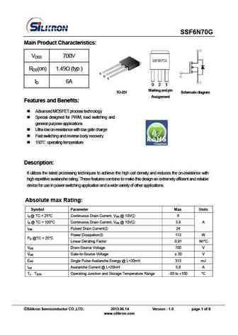
ssf6n70g.pdf
SSF6N70G Main Product Characteristics VDSS 700V RDS(on) 1.49 (typ.) ID 6A TO-251 Marking and p in S che ma ti c di ag ra m Assignment Features and Benefits Advanced MOSFET process technology Special designed for PWM, load switching and general purpose applications Ultra low on-resistance with low gate charge Fast switching and reverse body recovery
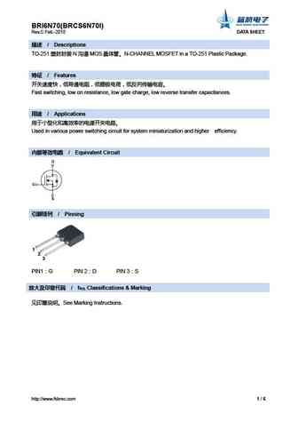
br6n70.pdf
BR6N70 Rev. F Jul.-2018 DATA SHEET / Descriptions TO-220 N MOS N-CHANNEL MOSFET in a TO-220 Plastic Package. / Features Fast switching, low on resistance, low gate charge, low reverse transfer capacitances. / Applications
cs6n70f b9d.pdf
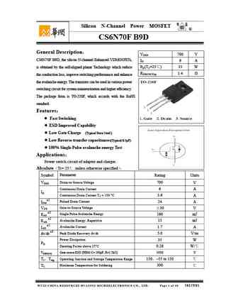
Silicon N-Channel Power MOSFET R CS6N70F B9D General Description VDSS 700 V CS6N70F B9D, the silicon N-channel Enhanced VDMOSFETs, ID 6 A PD(TC=25 ) 35 W is obtained by the self-aligned planar Technology which reduce RDS(ON)Typ 1.4 the conduction loss, improve switching performance and enhance the avalanche energy. The transistor can be used in various power
cs6n70 a3d-g.pdf
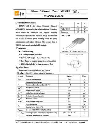
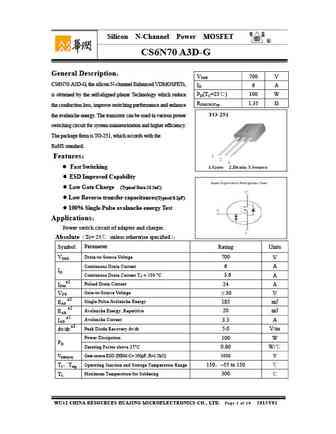
Silicon N-Channel Power MOSFET R CS6N70 A3D-G General Description VDSS 700 V CS6N70 A3D-G, the silicon N-channel Enhanced ID 6 A PD(TC=25 ) 100 W VDMOSFETs, is obtained by the self-aligned planar Technology RDS(ON)Typ 1.5 which reduce the conduction loss, improve switching performance and enhance the avalanche energy. The transistor can be used in various po
cs6n70 a3h.pdf
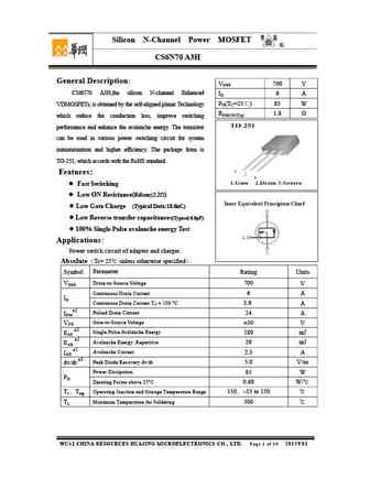
Silicon N-Channel Power MOSFET R CS6N70 A3H General Description VDSS 700 V CS6N70 A3H,the silicon N-channel Enhanced ID 6 A PD(TC=25 ) 85 W VDMOSFETs, is obtained by the self-aligned planar Technology RDS(ON)Typ 1.8 which reduce the conduction loss, improve switching performance and enhance the avalanche energy. The transistor can be used in various power swi
cs6n70 b3d1-g.pdf
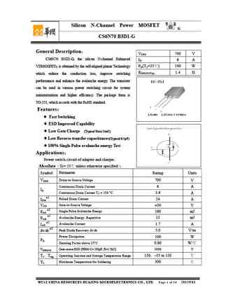
Silicon N-Channel Power MOSFET R CS6N70 B3D1-G General Description VDSS 700 V CS6N70 B3D1-G, the silicon N-channel Enhanced ID 6 A PD(TC=25 ) 100 W VDMOSFETs, is obtained by the self-aligned planar Technology RDS(ON)Typ 1.4 which reduce the conduction loss, improve switching performance and enhance the avalanche energy. The transistor can be used in various p
cs6n70 a4d-g.pdf
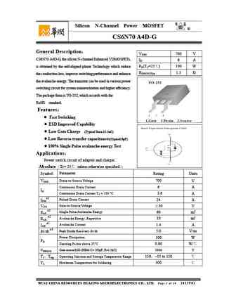
Silicon N-Channel Power MOSFET R CS6N70 A4D-G General Description VDSS 700 V CS6N70 A4D-G, the silicon N-channel Enhanced VDMOSFETs, ID 6 A PD(TC=25 ) 100 W is obtained by the self-aligned planar Technology which reduce RDS(ON)Typ 1.5 the conduction loss, improve switching performance and enhance the avalanche energy. The transistor can be used in various po
cs6n70f a9h.pdf
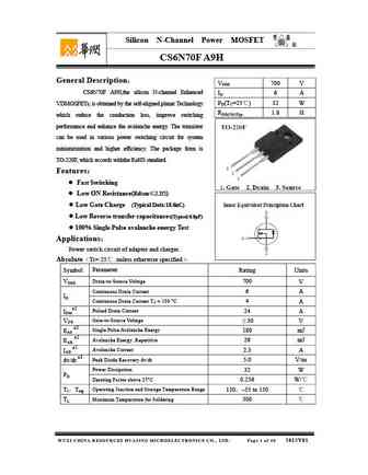
Silicon N-Channel Power MOSFET R CS6N70F A9H General Description VDSS 700 V CS6N70F A9H,the silicon N-channel Enhanced ID 6 A PD(TC=25 ) 32 W VDMOSFETs, is obtained by the self-aligned planar Technology RDS(ON)Typ 1.8 which reduce the conduction loss, improve switching performance and enhance the avalanche energy. The transistor can be used in various powe
cs6n70 a3d1-g.pdf
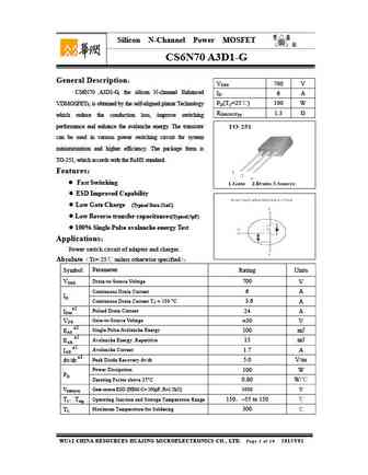
Silicon N-Channel Power MOSFET R CS6N70 A3D1-G General Description VDSS 700 V CS6N70 A3D1-G, the silicon N-channel Enhanced ID 6 A PD(TC=25 ) 100 W VDMOSFETs, is obtained by the self-aligned planar Technology RDS(ON)Typ 1.5 which reduce the conduction loss, improve switching performance and enhance the avalanche energy. The transistor can be used in various p
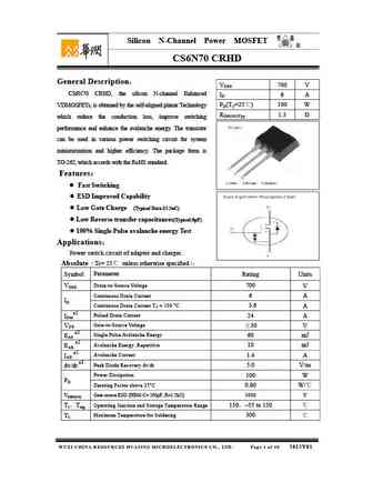
cs6n70 crhd.pdf
Silicon N-Channel Power MOSFET R CS6N70 CRHD General Description VDSS 700 V CS6N70 CRHD, the silicon N-channel Enhanced ID 6 A PD(TC=25 ) 100 W VDMOSFETs, is obtained by the self-aligned planar Technology RDS(ON)Typ 1.5 which reduce the conduction loss, improve switching performance and enhance the avalanche energy. The transistor can be used in various po
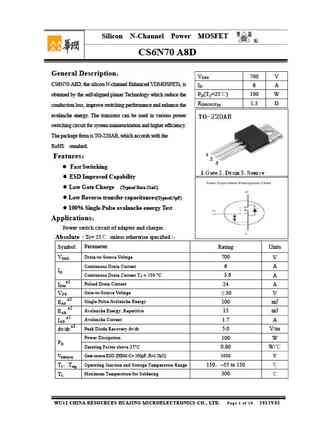
cs6n70 a8d.pdf
Silicon N-Channel Power MOSFET R CS6N70 A8D General Description VDSS 700 V CS6N70 A8D, the silicon N-channel Enhanced VDMOSFETs, is ID 6 A PD(TC=25 ) 100 W obtained by the self-aligned planar Technology which reduce the RDS(ON)Typ 1.5 conduction loss, improve switching performance and enhance the avalanche energy. The transistor can be used in various power s
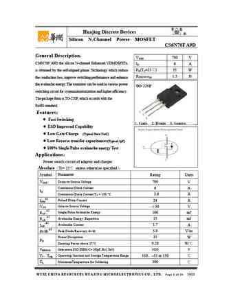
cs6n70f a9d.pdf
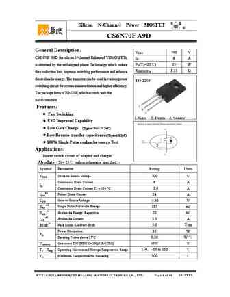
Huajing Discrete Devices R Silicon N-Channel Power MOSFET CS6N70F A9D General Description VDSS 700 V CS6N70F A9D the silicon N-channel Enhanced VDMOSFETs, ID 6 A PD(TC=25 ) 35 W is obtained by the self-aligned planar Technology which reduce RDS(ON)Typ 1.5 the conduction loss, improve switching performance and enhance the avalanche energy. The transistor can
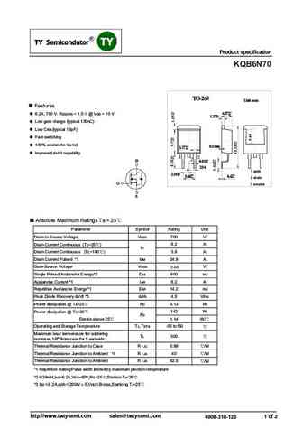
kqb6n70.pdf
SMD Type IC SMD Type IC SMD Type IC SMD Type IC SMD Type IC SMD Type IC SMD Type IC SMD Type Transistors SMD Type Transistors SMD Type Transistors SMD Type Transistors SMD Type Transistors SMD Type Transistors SMD Type Transistors SMDType SMDType IC Product specification KQB6N70 TO-263 Unit mm Features 4.57+0.2 6.2A, 700 V. RDS(ON) =1.5 @VGS =10V -0.2 +0.1 1.27-0.1 Low
ftk6n70p f d i.pdf
SEMICONDUCTOR FTK6N70P/F/D/I TECHNICAL DATA Power MOSFET 6.0 Amps, 700 Volts I N-CHANNEL MOSFET 1 TO - 251 D 1 DESCRIPTION TO - 252 The FTK6N70 is a high voltage MOSFET and is designed to have better characteristics, such as fast switching time, low gate P charge, low on-state resistance and have a high rugged avalanche characteristics. This power MOSFET is usually us
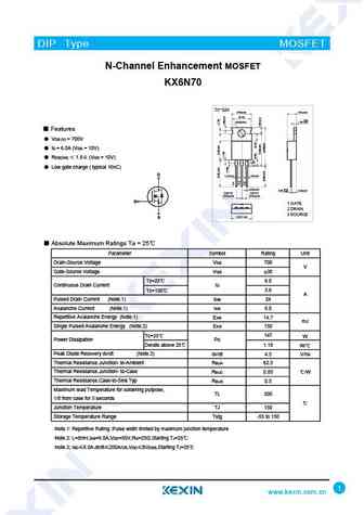
kx6n70.pdf
DIP Type MOSFET N-Channel Enhancement MOSFET KX6N70 TO-220 9.90 0.20 4.50 0.20 (8.70) +0.10 3.60 0.10 1.30 0.05 Features VDS (V) = 700V ID = 6.0A (VGS = 10V) RDS(ON) 1.8 (VGS = 10V) Low gate charge ( typical 16nC) D 1.27 0.10 1.52 0.10 2 1 3 0.80 0.10 +0.10 0.50 0.05 2.40 0.20 2.54TYP 2.54TYP [2.54 0.20] [2.54 0.20] G
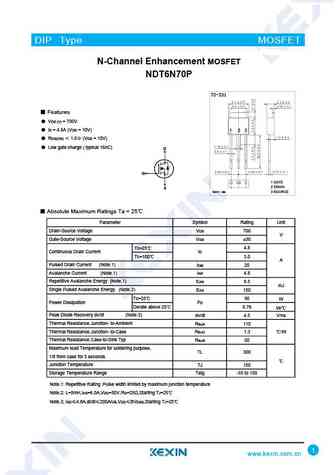
ndt6n70p.pdf
DIP Type MOSFET N-Channel Enhancement MOSFET NDT6N70P TO-251 Features VDS (V) = 700V ID = 4.8A (VGS = 10V) 1 2 3 RDS(ON) 1.8 (VGS = 10V) Low gate charge ( typical 16nC) D 1 3 2 G S Unit mm Absolute Maximum Ratings Ta = 25 Parameter Symbol Rating Unit Drain-Source Voltage VDS 700 V Gate-Source Voltage VGS 30 Tc=25 4.8 Continuou
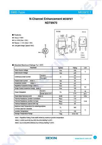
ndt6n70.pdf
SMD Type MOSFET N-Channel Enhancement MOSFET NDT6N70 TO-252 Unit mm + 0.15 Features 6.50- 0.15 +0.1 2.30 -0.1 + 0.2 5.30- 0.2 +0.8 0.50 -0.7 VDS (V) = 700V ID = 4.8A (VGS = 10V) RDS(ON) 1.8 (VGS = 10V) D 0.127 Low gate charge ( typical 16nC) +0.1 0.80 -0.1 max G + 0.1 1 Gate 2.3 0.60- 0.1 + 0.15 4.60- 0.15 2 Drain S 3 Source Absol
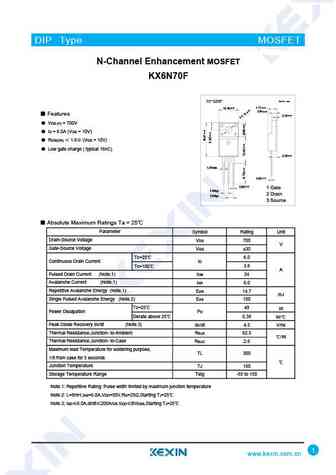
kx6n70f.pdf
DIP Type MOSFET N-Channel Enhancement MOSFET KX6N70F Unit mm TO-220F 0.20 0.20 0.20 2.54 Features 0.20 0.70 VDS (V) = 700V ID = 6.0A (VGS = 10V) RDS(ON) 1.8 (VGS = 10V) Low gate charge ( typical 16nC) 0.20 2.76 1.47max 0.20 0.50 0.20 0.80 2.54typ 2.54typ Absolute Maximum Ratings Ta = 25 Parameter Symbol Rating Unit
svf6n70mjg svf6n70dtr svf6n70k svf6n70mn.pdf
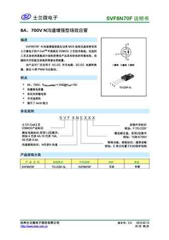
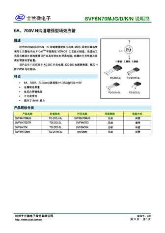
SVF6N70MJG/D/K/N 6A 700V N 2 SVF6N70MJG/D/K/N N MOS 1 F-CellTM VDMOS 3 1.
mdib6n70cth.pdf
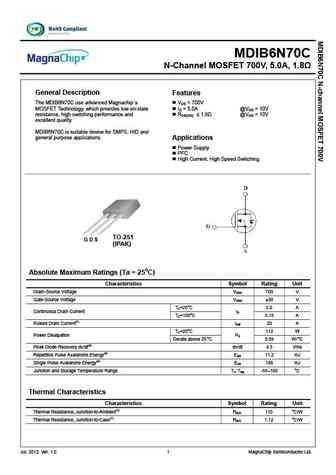
MDIB6N70C N-Channel MOSFET 700V, 5.0A, 1.8 General Description Features The MDIB6N70C use advanced Magnachip s VDS = 700V MOSFET Technology, which provides low on-state @VGS = 10V ID = 5.0A resistance, high switching performance and @VGS = 10V RDS(ON) 1.8 excellent quality. MDIB6N70C is suitable device for SMPS, HID and general purpose applications. Applications
msf6n70.pdf
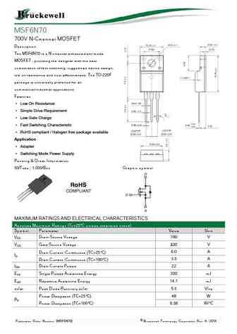
MSF6N70 700V N-Channel MOSFET Description The MSF6N70 is a N-channel enhancement-mode MOSFET , providing the designer with the best combination of fast switching, ruggedized device design, low on-resistance and cost effectiveness. The TO-220F package is universally preferred for all commercial-industrial applications Features Low On Resistance Simple Drive Requirem
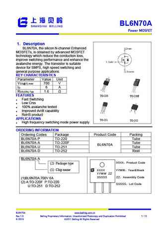
bl6n70a-p bl6n70a-a bl6n70a-u bl6n70a-d.pdf
BL6N70A Power MOSFET 1 Description Step-Down Converter BL6N70A, the silicon N-channel Enhanced , MOSFETs, is obtained by advanced MOSFET technology which reduce the conduction loss, improve switching performance and enhance the avalanche energy. The transistor is suitable device for SMPS, high speed switching and general purpose applications. KEY CHARACTERISTICS Pa
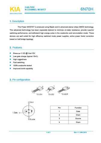
kia6n70h.pdf
5.8A,700V N-CHANNELMOSFET 6N70H KIA KIA KIA SEMICONDUCTORS SEMICONDUCTORS SEMICONDUCTORS 1.Description This Power MOSFETis produced using Maple semi s advanced planar stripe DMOStechnology. This advanced technology has been especially tailored to minimize on-state resistance, provide superior switching performance, and withstand high energy pulse in the avalanche and commutation m
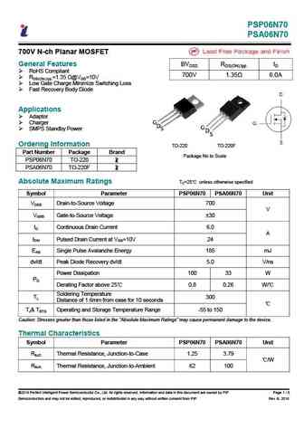
psp06n70 psa06n70.pdf
PSP06N70 PSA06N70 700V N-ch Planar MOSFET General Features BVDSS RDS(ON),typ. ID RoHS Compliant 700V 1.35 6.0A RDS(ON),typ.=1.35 @VGS=10V Low Gate Charge Minimize Switching Loss Fast Recovery Body Diode Applications Adaptor Charger G D S G D SMPS Standby Power S Ordering Information TO-220 TO-220F Part Number Package Brand
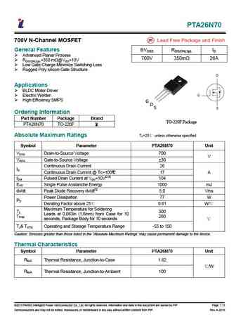
pta26n70.pdf
PTA26N70 700V N-Channel MOSFET General Features BVDSS RDS(ON),typ. ID Advanced Planar Process 700V 350m 26A RDS(ON),typ.=350 m @VGS=10V Low Gate Charge Minimize Switching Loss Rugged Poly silicon Gate Structure Applications BLDC Motor Driver Electric Welder High Efficiency SMPS G D S Ordering Information Part Number Package Brand TO-220F Package P
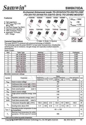
sw6n70da swn6n70da swsi6n70da swui6n70da swd6n70da swf6n70da swi6n70da swnx6n70da swp6n70da swqi6n70da swmqi6n70da.pdf
SW6N70DA N-channel Enhanced mode TO-251N/S/U/TO-252/TO-220F /TO-251/TO-251NX/TO-220/TO-251Q /TO-251MQ MOSFET TO251N TO251S TO251U TO252 TO220F Features BVDSS 700V l High ruggedness ID 6A l Low RDS(ON) (Typ 1.7 ) 1 1 RDS(ON) 1.7 1 1 @VGS=10V 2 2 2 2 1 3 3 2 3 3 l Low Gate Charge (Typ 26nC) 3 2 l Improved dv/dt Capability TO220 TO251Q TO251NX TO251 TO251MQ l
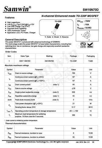
swf16n70d.pdf
SW16N70D N-channel Enhanced mode TO-220F MOSFET Features TO-220F BVDSS 700V High ruggedness Low RDS(ON) (Typ 0.54 )@VGS=10V ID 16A Low Gate Charge (Typ 67nC) RDS(ON) 0.54 Improved dv/dt Capability 100% Avalanche Tested 2 1 Application LED, PC Power, Charger 2 3 1 1. Gate 2. Drain 3. Source General Description 3 This pow
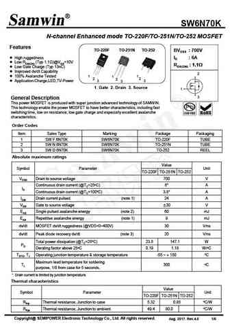
swf6n70k swn6n70k swd6n70k.pdf
SW6N70K N-channel Enhanced mode TO-220F/TO-251N/TO-252 MOSFET Features TO-220F TO-251N TO-252 BVDSS 700V High ruggedness ID 6A Low RDS(ON) (Typ 1.1 )@VGS=10V RDS(ON) 1.1 Low Gate Charge (Typ 13nC) Improved dv/dt Capability 2 100% Avalanche Tested 1 1 1 2 2 2 Application Charger,LED,TV-Power 3 3 3 1. Gate 2. Drain 3. Source 1
sw6n70k swf6n70k swn6n70k swd6n70k.pdf
SW6N70K N-channel Enhanced mode TO-220F/TO-251N/TO-252 MOSFET Features TO-251N TO-220F TO-252 BVDSS 700V High ruggedness ID 6A Low RDS(ON) (Typ 1.1 )@VGS=10V RDS(ON) 1.1 Low Gate Charge (Typ 13nC) Improved dv/dt Capability 2 100% Avalanche Tested 1 1 1 2 2 2 Application Charge,LED,TV-Power 3 3 3 1. Gate 2. Drain 3. Source
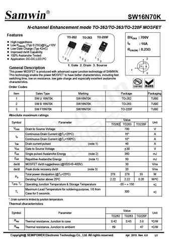
swu16n70k swb16n70k swf16n70k.pdf
SW16N70K N-channel Enhancement mode TO-262/TO-263/TO-220F MOSFET Features TO-262 TO-220F BVDSS 700V TO-263 High ruggedness ID 16A Low RDS(ON) (Typ 0.23 )@VGS=10V Low Gate Charge (Typ 42nC) RDS(ON) 0.23 Improved dv/dt Capability 100% Avalanche Tested 1 1 1 2 2 Application DC-DC,LED,PC 2 2 3 3 3 1. Gate 2. Drain 3. S
swf6n70d.pdf
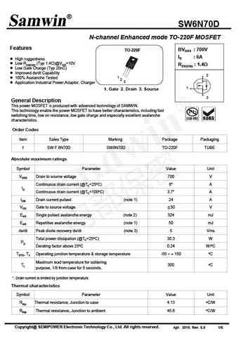
SW6N70D N-channel Enhanced mode TO-220F MOSFET Features BVDSS 700V TO-220F ID 6A High ruggedness Low RDS(ON) (Typ 1.4 )@VGS=10V RDS(ON) 1.4 Low Gate Charge (Typ 20nC) Improved dv/dt Capability 2 1 100% Avalanche Tested 2 3 Application Industrial Power,Adaptor, Charger 1 1. Gate 2. Drain 3. Source 3 General Description
swn6n70da swsi6n70da swui6n70da swd6n70da swf6n70da swi6n70da swnx6n70da swp6n70da swqi6n70da swmqi6n70da.pdf
SW6N70DA N-channel Enhanced mode TO-251N/S/U/TO-252/TO-220F /TO-251/TO-251NX/TO-220/TO-251Q /TO-251MQ MOSFET TO251N TO251S TO251U TO252 TO220F Features BVDSS 700V l High ruggedness ID 6A l Low RDS(ON) (Typ 1.7 ) 1 1 RDS(ON) 1.7 1 1 @VGS=10V 2 2 2 2 1 3 3 2 3 3 l Low Gate Charge (Typ 26nC) 3 2 l Improved dv/dt Capability TO220 TO251Q TO251NX TO251 TO251MQ l
swf6n70db swd6n70db swn6n70db.pdf
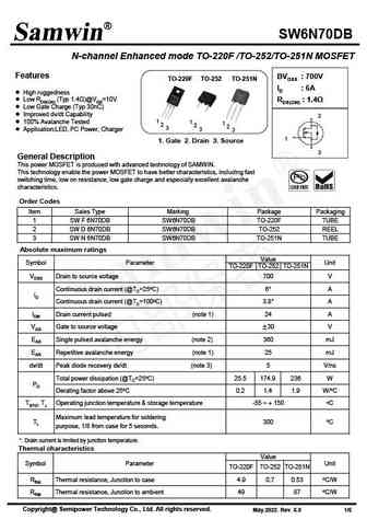
SW6N70DB N-channel Enhanced mode TO-220F /TO-252/TO-251N MOSFET Features BVDSS 700V TO-220F TO-252 TO-251N ID 6A High ruggedness Low RDS(ON) (Typ 1.4 )@VGS=10V RDS(ON) 1.4 Low Gate Charge (Typ 30nC) Improved dv/dt Capability 2 1 100% Avalanche Tested 1 1 2 2 2 3 Application LED, PC Power, Charger 3 3 1 1. Gate 2. Drain 3. Source 3 Gen
srm6n70.pdf
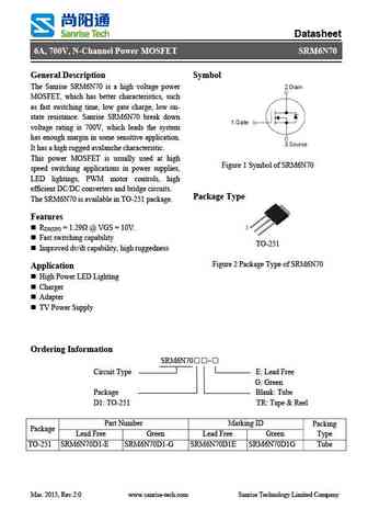
Datasheet 6A, 700V, N-Channel Power MOSFET SRM6N70 General Description Symbol The Sanrise SRM6N70 is a high voltage power MOSFET, which has better characteristics, such as fast switching time, low gate charge, low on- state resistance. Sanrise SRM6N70 break down voltage rating is 700V, which leads the system has enough margin in some sensitive application. It has a high rugged a
hcu6n70s.pdf
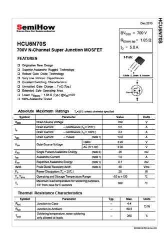
Dec 2013 BVDSS = 700 V RDS(on) typ = 1.05 HCU6N70S ID = 5.0 A 700V N-Channel Super Junction MOSFET I-PAK FEATURES Originative New Design 1 Superior Avalanche Rugged Technology 2 3 Robust Gate Oxide Technology 1.Gate 2. Drain 3. Source Very Low Intrinsic Capacitances Excellent Switching Characteristics Unrivalled Gate Charge 7 nC (Typ.) Extended Safe Operati
hfn6n70u.pdf
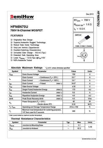
Dec 2012 BVDSS = 700 V RDS(on) typ = 1.8 HFN6N70U ID = 6.0 A 700V N-Channel MOSFET SOT-82 FEATURES Originative New Design Superior Avalanche Rugged Technology 1 2 3 Robust Gate Oxide Technology 1.Gate 2. Drain 3. Source Very Low Intrinsic Capacitances Excellent Switching Characteristics Unrivalled Gate Charge 16.0 nC (Typ.) Extended Safe Operating Area Lo
hfp6n70u.pdf
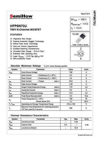
March 2013 BVDSS = 700 V RDS(on) typ = 1.8 HFP6N70U ID = 6.0 A 700V N-Channel MOSFET TO-220 FEATURES Originative New Design Superior Avalanche Rugged Technology 1 2 3 Robust Gate Oxide Technology 1.Gate 2. Drain 3. Source Very Low Intrinsic Capacitances Excellent Switching Characteristics Unrivalled Gate Charge 16.0 nC (Typ.) Extended Safe Operating Area
hfs6n70u.pdf
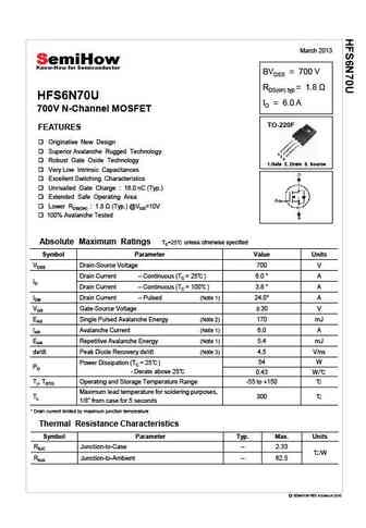
March 2013 BVDSS = 700 V RDS(on) typ = 1.8 HFS6N70U ID = 6.0 A 700V N-Channel MOSFET TO-220F FEATURES Originative New Design Superior Avalanche Rugged Technology 1 2 3 Robust Gate Oxide Technology 1.Gate 2. Drain 3. Source Very Low Intrinsic Capacitances Excellent Switching Characteristics Unrivalled Gate Charge 16.0 nC (Typ.) Extended Safe Operating Area
hfd6n70u.pdf
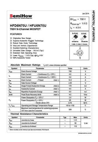
Jan 2014 BVDSS = 700 V RDS(on) typ HFD6N70U / HFU6N70U ID = 4.8 A 700V N-Channel MOSFET D-PAK I-PAK FEATURES 2 1 Originative New Design 1 3 2 3 Superior Avalanche Rugged Technology HFD6N70U HFU6N70U Robust Gate Oxide Technology 1.Gate 2. Drain 3. Source Very Low Intrinsic Capacitances Excellent Switching Characteristics Unrivalled Gate Charge 16.0 nC
tmd6n70.pdf
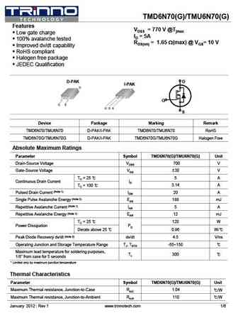
TMD6N70(G)/TMU6N70(G) Features VDSS = 770 V @Tjmax Low gate charge ID = 5A 100% avalanche tested RDS(on) = 1.65 W(max) @ VGS= 10 V Improved dv/dt capability RoHS compliant Halogen free package JEDEC Qualification D-PAK D I-PAK G S Device Package Marking Remark TMD6N70/TMU6N70 D-PAK/I-PAK TMD6N70/TMU6N70 RoHS TMD6N70G/TMU6N70G D-PAK/I-PAK
tmp6n70 tmpf6n70.pdf
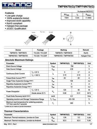
TMP6N70(G)/TMPF6N70(G) N-channel MOSFET Features BVDSS ID RDS(on) Low gate charge 700V 5.0A
tmd6n70g tmu6n70g tmd6n70 tmu6n70.pdf
TMD6N70(G)/TMU6N70(G) Features VDSS = 770 V @Tjmax Low gate charge ID = 5A 100% avalanche tested RDS(on) = 1.65 W(max) @ VGS= 10 V Improved dv/dt capability RoHS compliant Halogen free package JEDEC Qualification D-PAK D I-PAK G S Device Package Marking Remark TMD6N70/TMU6N70 D-PAK/I-PAK TMD6N70/TMU6N70 RoHS TMD6N70G/TMU6N70G D-PAK/I-PAK
wml16n70sr wmk16n70sr wmm16n70sr wmn16n70sr wmp16n70sr wmo16n70sr.pdf
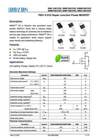
WML16N70SR, W 70SR, WM SR WMK16N7 MM16N70S WMN16N70SR, WMP16N7 MO16N70S 70SR, WM SR 700V 0.31 S unction P MOSFET 0 Super Ju Power M T Descrip ption WMOSTM SR is Wa new generation super ayon s w junction MOSFET fa that is utilizing charge M amily S balance te or extremely esistance echnology fo y low on-re D S D G G G S D G T and low ga charge perfo
wml16n70d1b.pdf
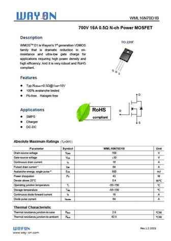
WML16N70D1B 700V 16A 0.5 N-ch Power MOSFET Description TO-220F WMOSTM D1 is Wayon s 1st generation VDMOS family that is dramatic reduction in on- resistance and ultra-low gate charge for applications requiring high power density and high efficiency. And it is very robust and RoHS compliant. G D S Features Typ.R =0.5 @V =10V DS(on) GS 100% avalanche t
cs6n70a3d-g.pdf
Silicon N-Channel Power MOSFET R CS6N70 A3D-G General Description VDSS 700 V CS6N70 A3D-G, the silicon N-channel Enhanced VDMOSFETs, ID 6 A PD(TC=25 ) 100 W is obtained by the self-aligned planar Technology which reduce RDS(ON)Typ 1.35 the conduction loss, improve switching performance and enhance the avalanche energy. The transistor can be used in various powe
cs6n70fb9d.pdf
Silicon N-Channel Power MOSFET R CS6N70F B9D General Description VDSS 700 V CS6N70F B9D, the silicon N-channel Enhanced VDMOSFETs, ID 6 A PD(TC=25 ) 35 W is obtained by the self-aligned planar Technology which reduce RDS(ON)Typ 1.4 the conduction loss, improve switching performance and enhance the avalanche energy. The transistor can be used in various power
cs6n70fa9d.pdf
Silicon N-Channel Power MOSFET R CS6N70F A9D General Description VDSS 700 V CS6N70F A9D the silicon N-channel Enhanced VDMOSFETs, ID 6 A PD(TC=25 ) 35 W is obtained by the self-aligned planar Technology which reduce RDS(ON)Typ 1.35 the conduction loss, improve switching performance and enhance the avalanche energy. The transistor can be used in various power
cs6n70a4d-g.pdf
Silicon N-Channel Power MOSFET R CS6N70 A4D-G General Description VDSS 700 V CS6N70 A4D-G, the silicon N-channel Enhanced VDMOSFETs, ID 6 A PD(TC=25 ) 100 W is obtained by the self-aligned planar Technology which reduce RDS(ON)Typ 1.5 the conduction loss, improve switching performance and enhance the avalanche energy. The transistor can be used in various po
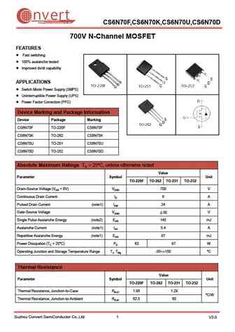
cs6n70f cs6n70k cs6n70u cs6n70d.pdf
nvert Suzhou Convert Semiconductor Co ., Ltd. CS6N70F,CS6N70K,CS6N70U,CS6N70D 700V N-Channel MOSFET FEATURES Fast switching 100% avalanche tested Improved dv/dt capability APPLICATIONS Switch Mode Power Supply (SMPS) Uninterruptible Power Supply (UPS) Power Factor Correction (PFC) Device Marking and Package Information Device Package Marking CS6N70F TO-220F
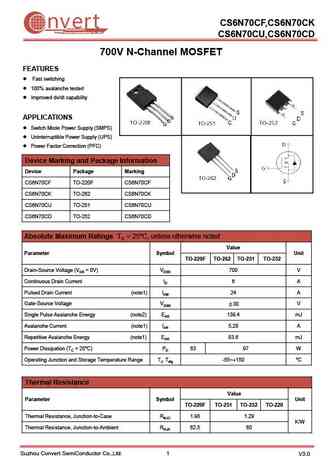
cs6n70cf cs6n70ck cs6n70cu cs6n70cd.pdf
CS6N70CF,CS6N70CK nvert Suzhou Convert Semiconductor Co ., Ltd. CS6N70CU,CS6N70CD 700V N-Channel MOSFET FEATURES Fast switching 100% avalanche tested Improved dv/dt capability APPLICATIONS Switch Mode Power Supply (SMPS) Uninterruptible Power Supply (UPS) Power Factor Correction (PFC) Device Marking and Package Information Device Package Marking CS6N70CF
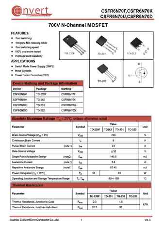
csfr6n70f csfr6n70k csfr6n70u csfr6n70d.pdf
CSFR6N70F,CSFR6N70K nvert Suzhou Convert Semiconductor Co ., Ltd. CSFR6N70U,CSFR6N70D 700V N-Channel MOSFET FEATURES Fast switching Integrate fast recovery diode Fast switching speed 100% avalanche tested Improved dv/dt capability APPLICATIONS Switch Mode Power Supply (SMPS) Motor Controls Power Factor Correction (PFC) Device Marking and Package In
fir6n70fg.pdf
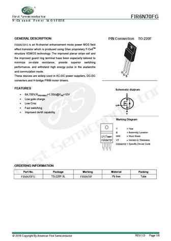
FIR6N70FG N - Ch a n n el P o w e r M O S F ET-E GENERAL DESCRIPTION PIN Connection TO-220F is an N-channel enhancement mode power MOS field FIR6N70FG effect transistor which is produced using Silan proprietary F-CellTM structure VDMOS technology. The improved planar stripe cell and the improved guard ring terminal have been especially tailored to minimize on-state resistance, pr
slp6n70u slf6n70u.pdf
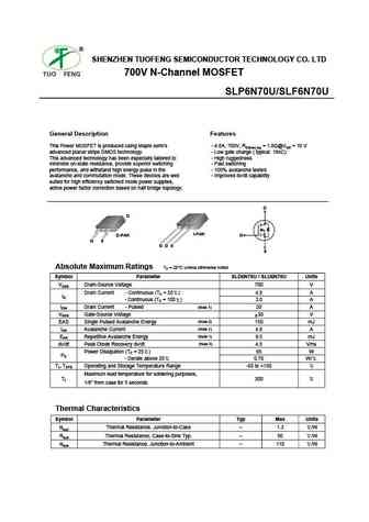
SHENZHEN TUOFENG SEMICONDUCTOR TECHNOLOGY CO. LTD 700V N-Channel MOSFET SLP6N70U/SLF6N70U SLP6N70U/SLF6N70U General Description Features This Power MOSFET is produced using Maple semi s - 4.8A, 700V, RDS(on) typ = 1.8 @VGS = 10 V advanced planar stripe DMOS technology. - Low gate charge ( typical 16nC) This advanced technology has been especially tailored to - High ruggedness minimi
hm6n70 hm6n70f.pdf
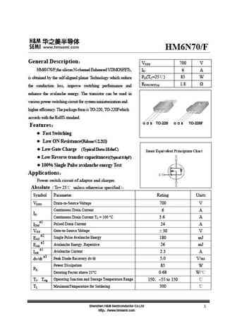
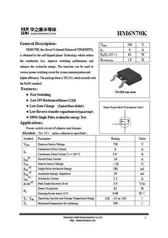
HM6N70/F General Description VDSS 700 V HM6N70/F,the silicon N-channel Enhanced VDMOSFETs, ID 6 A PD(TC=25 ) 85 W is obtained by the self-aligned planar Technology which reduce RDS(ON)Typ 1.8 the conduction loss, improve switching performance and enhance the avalanche energy. The transistor can be used in various power switching circuit for system miniaturization a
hm6n70i.pdf
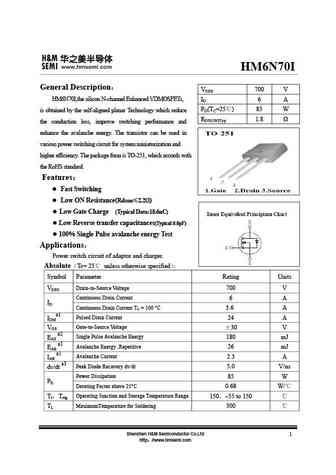
HM6N70I General Description VDSS 700 V ,the silicon N-channel Enhanced VDMOSFETs, ID 6 A PD(TC=25 ) 85 W is obtained by the self-aligned planar Technology which reduce RDS(ON)Typ 1.8 the conduction loss, improve switching performance and enhance the avalanche energy. The transistor can be used in various power switching circuit for system miniaturiz
hm6n70k.pdf
HM6N70K General Description VDSS 700 V HM6N70K, the silicon N-channel Enhanced VDMOSFETs, ID 6 A PD(TC=25 ) 85 W is obtained by the self-aligned planar Technology which reduce RDS(ON)Typ 1.8 the conduction loss, improve switching performance and enhance the avalanche energy. The transistor can be used in various power switching circuit for system miniaturization an
h6n70p h6n70f.pdf
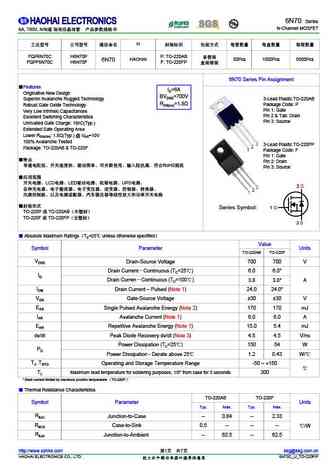
6N70 Series N-Channel MOSFET 6A, 700V, N H FQP6N70C H6N70P P TO-220AB HAOHAI 50Pcs 1000Pcs 5000Pcs 6N70 FQPF6N70C H6N70F F TO-220FP 6N70 Series Pin Assignment Features ID=6A Originative New Design BVD
h6n70u h6n70d.pdf
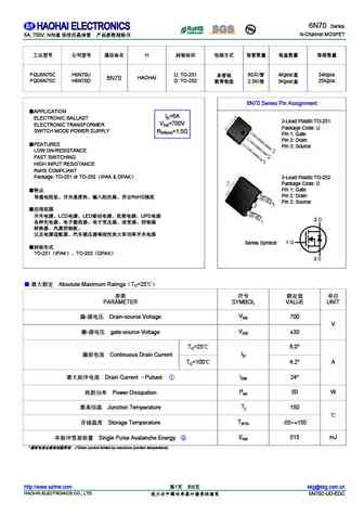
6N70 Series N-Channel MOSFET 6A, 700V, N H FQU6N70C H6N70U U TO-251 80 / 4Kpcs/ 24Kpcs HAOHAI 6N70 FQD6N70C H6N70D D TO-252 25Kpcs 2.5K/ 5Kpcs/ 6N70 Series Pin Assignment APPLICATION ID=6A
6n70a.pdf
INCHANGE Semiconductor isc N-Channel MOSFET Transistor 6N70A FEATURES Drain Current I = 6A@ T =25 D C Drain Source Voltage V = 700V(Min) DSS Avalanche Energy Specified Fast Switching Simple Drive Requirements Minimum Lot-to-Lot variations for robust device performance and reliable operation DESCRITION Switch mode power supply. ABSOLUTE MAXIMUM RATINGS(T =2
Otros transistores... 2N70ZL, 2N70K, 3N70, 3N70A, 3N70K, 4N70, 4N70K, 5N70K, IRF1010E, 7N70, 8N70, 9N70, 10N70, 12N70, 15N70, 6N65Z, 7N65A
History: AO4826
🌐 : EN ES РУ
Liste
Recientemente añadidas las descripciónes de los transistores:
MOSFET: AUP060N055 | AUP056N10 | AUP056N08BGL | AUP052N085 | AUP045N12 | AUP039N10 | AUP034N10 | AUP034N06 | AUP033N08BG | AUP026N085 | AUN084N10 | AUN065N10 | AUN063N10 | AUN062N08BG | AUN060N08AG | AUN053N10
Popular searches
2sd315 | a1013 | 2sb554 | 2sd2560 | 2sc2078 transistor | bc558 datasheet | p75nf75 mosfet | ao4407a
