8N70 MOSFET Equivalente. Reemplazo. Hoja de especificaciones. Principales características
Número de Parte: 8N70
Tipo de FET: MOSFET
Polaridad de transistor: N
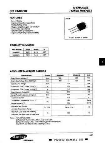
ESPECIFICACIONES MÁXIMAS
Pdⓘ - Máxima
disipación de potencia: 147 W
|Vds|ⓘ - Voltaje máximo drenador-fuente: 700 V
|Vgs|ⓘ - Voltaje máximo fuente-puerta: 30 V
|Id|ⓘ - Corriente continua
de drenaje: 8 A
Tjⓘ - Temperatura máxima de unión: 150 °C
CARACTERÍSTICAS ELÉCTRICAS
trⓘ - Tiempo
de subida: 115 nS
Cossⓘ - Capacitancia de salida: 124 pF
RDSonⓘ - Resistencia estado encendido drenaje a fuente: 1.2 Ohm
Encapsulados: TO-220
TO-220F
TO-220F1
Búsqueda de reemplazo de 8N70 MOSFET
- Selecciónⓘ de transistores por parámetros
8N70 datasheet
..1. Size:229K utc
8n70.pdf 
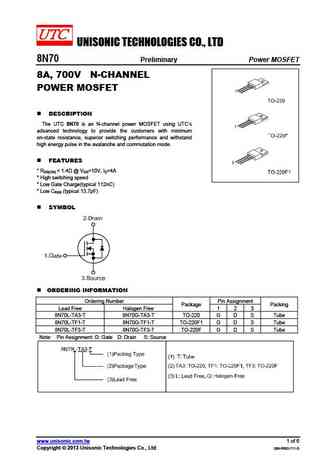
UNISONIC TECHNOLOGIES CO., LTD 8N70 Preliminary Power MOSFET 8A, 700V N-CHANNEL POWER MOSFET DESCRIPTION The UTC 8N70 is an N-channel power MOSFET using UTC s advanced technology to provide the customers with minimum on-state resistance, superior switching performance and withstand high energy pulse in the avalanche and commutation mode. FEATURES * RDS(ON)
0.2. Size:3733K taiwansemi
tsm8n70ci.pdf
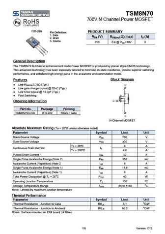
TSM8N70 700V N-Channel Power MOSFET ITO-220 PRODUCT SUMMARY Pin Definition 1. Gate VDS (V) RDS(on)( )(max) ID (A) 2. Drain 3. Source 700 0.9 @ VGS =10V 8 General Description The TSM8N70 N-Channel enhancement mode Power MOSFET is produced by planar stripe DMOS technology. This advanced technology has been especially tailored to minimize on-state resistance, provide sup
0.3. Size:417K cystek
mtn8n70fp.pdf
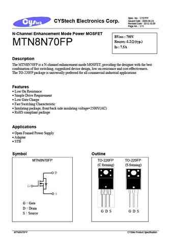
Spec. No. C727FP Issued Date 2009.06.23 CYStech Electronics Corp. Revised Date 2012.10.08 Page No. 1/11 N-Channel Enhancement Mode Power MOSFET BVDSS 700V RDS(ON) 1.2 (typ.) MTN8N70FP ID 7.5A Description The MTN8N70FP is a N-channel enhancement-mode MOSFET, providing the designer with the best combination of fast switching, ruggedized device design, low on-r
0.4. Size:242K crhj
cs8n70f a9h2-g.pdf
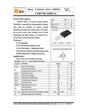
Silicon N-Channel Power MOSFET R CS8N70F A9H2-G General Description VDSS 700 V CS8N70F A9H2-G , the silicon N-channel Enhanced ID 8 A PD(TC=25 ) 48 W VDMOSFETs, is obtained by the self-aligned planar Technology RDS(ON)Typ 1 which reduce the conduction loss, improve switching performance and enhance the avalanche energy. The transistor can be used in various
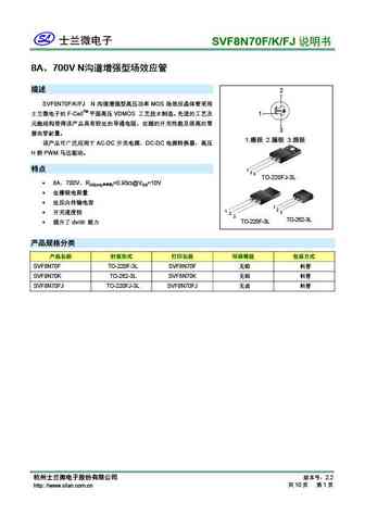
0.6. Size:312K silan
svf8n70fjh.pdf
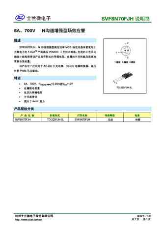
SVF8N70FJH 8A 700V N 2 SVF8N70FJH N MOS F-CellTM VDMOS 1 3 1. 2.
0.7. Size:144K hy
hy8n70t.pdf
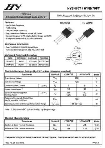
HY8N70T / HY8N70FT 700V / 8A 700V, RDS(ON)=1.2W@VGS=10V, ID=4.0A N-Channel Enhancement Mode MOSFET Features TO-220AB ITO-220AB Low On-State Resistance Fast Switching Low Gate Charge & Low CRSS Fully Characterized Avalanche Voltage and Current Specially Desigened for AC Adapter, Battery Charger and SMPS In compliance with EU RoHs 2002/95/EC Directives 1
0.8. Size:710K samwin
sw8n70d swf8n70d swj8n70d.pdf

SW8N70D N-channel Enhanced mode TO-220F/TO-262N MOSFET Features TO-220F TO-262N BVDSS 700V High ruggedness ID 8A Low RDS(ON) (Typ 1.0m )@VGS=10 RDS(ON) 1.0 Low Gate Charge (Typ 37nC) Improved dv/dt Capability 2 100% Avalanche Tested 1 1 2 2 Application Electronic Ballast , Motor 3 3 Control , Synchronous Rectification, Inverter
0.9. Size:613K samwin
swt38n70k.pdf
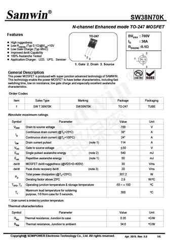
SW38N70K N-channel Enhanced mode TO-247 MOSFET Features TO-247 BVDSS 700V ID 38A High ruggedness Low RDS(ON) (Typ 0.1 )@VGS=10V RDS(ON) 0.1 Low Gate Charge (Typ 96nC) Improved dv/dt Capability 2 1 100% Avalanche Tested 2 1 3 Application Charger LED UPS Servicer 1. Gate 2. Drain 3. Source 3 General Description This
0.10. Size:791K samwin
swf8n70k swd8n70k.pdf
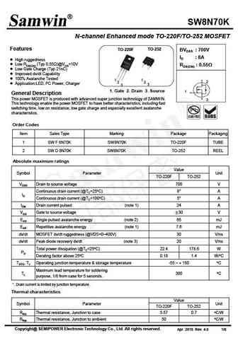
SW8N70K N-channel Enhanced mode TO-220F/TO-252 MOSFET Features TO-252 TO-220F BVDSS 700V ID 8A High ruggedness Low RDS(ON) (Typ 0.55 )@VGS=10V RDS(ON) 0.55 Low Gate Charge (Typ 21nC) Improved dv/dt Capability 100% Avalanche Tested 1 1 2 2 2 Application LED, PC Power, Charger 3 3 1. Gate 2. Drain 3. Source 1 General
0.11. Size:775K samwin
swf8n70d swj8n70d.pdf
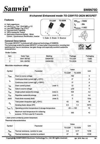
SW8N70D N-channel Enhanced mode TO-220F/TO-262N MOSFET Features TO-220F TO-262N BVDSS 700V High ruggedness ID 8A Low RDS(ON) (Typ 1.0m )@VGS=10 RDS(ON) 1.0 Low Gate Charge (Typ 37nC) Improved dv/dt Capability 2 100% Avalanche Tested 1 1 2 2 Application Electronic Ballast , Motor 3 3 Control , Synchronous Rectification, Inverter
0.12. Size:183K semihow
hfs8n70s.pdf
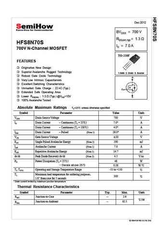
Dec 2012 BVDSS = 700 V RDS(on) typ HFS8N70S ID = 7.0 A 700V N-Channel MOSFET TO-220F FEATURES 1 Originative New Design 2 3 Superior Avalanche Rugged Technology 1.Gate 2. Drain 3. Source Robust Gate Oxide Technology Very Low Intrinsic Capacitances Excellent Switching Characteristics Unrivalled Gate Charge 22 nC (Typ.) Extended Safe Operating Area Lo
0.13. Size:198K semihow
hfp8n70u.pdf
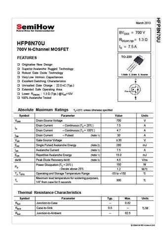
March 2013 BVDSS = 700 V RDS(on) typ = 1.3 HFP8N70U ID = 7.5 A 700V N-Channel MOSFET TO-220 FEATURES Originative New Design Superior Avalanche Rugged Technology 1 2 3 Robust Gate Oxide Technology 1.Gate 2. Drain 3. Source Very Low Intrinsic Capacitances Excellent Switching Characteristics Unrivalled Gate Charge 22.0 nC (Typ.) Extended Safe Operating Area
0.14. Size:201K semihow
hfd8n70u.pdf
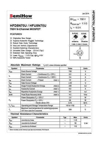
Jan 2014 BVDSS = 700 V RDS(on) typ = 1.3 HFD8N70U / HFU8N70U ID = 6.0 A 700V N-Channel MOSFET D-PAK I-PAK FEATURES 2 1 Originative New Design 1 3 2 3 Superior Avalanche Rugged Technology HFD8N70U HFU8N70U Robust Gate Oxide Technology 1.Gate 2. Drain 3. Source Very Low Intrinsic Capacitances Excellent Switching Characteristics Unrivalled Gate Charge 22.0 nC
0.15. Size:307K semihow
hfs8n70u.pdf
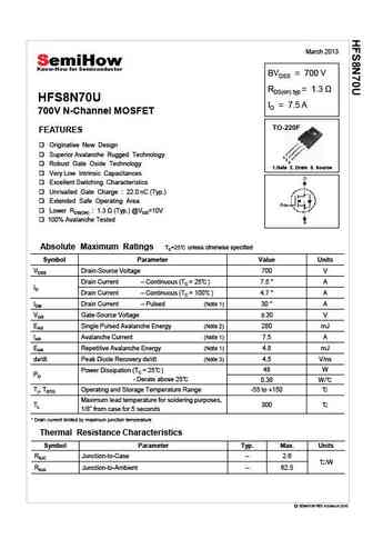
March 2013 BVDSS = 700 V RDS(on) typ = 1.3 HFS8N70U ID = 7.5 A 700V N-Channel MOSFET TO-220F FEATURES Originative New Design Superior Avalanche Rugged Technology 1 2 3 Robust Gate Oxide Technology 1.Gate 2. Drain 3. Source Very Low Intrinsic Capacitances Excellent Switching Characteristics Unrivalled Gate Charge 22.0 nC (Typ.) Extended Safe Operating Area
0.16. Size:670K way-on
wmm08n70c4 wml08n70c4 wmo08n70c4 wmn08n70c4 wmp08n70c4 wmk08n70c4.pdf

WMM0 70C4, MO08N70C 08N70C4, WML08N7 WM C4 WMN0 70C4, MK08N70C 08N70C4, WMP08N7 WM C4 700V 0.65 S T V Super Junction Power MOSFET Descrip ption WMOSTM C4 is Wa 4th generation super ayon s n junction MOSFET fa that is utilizing charge M amily S balance te or extremely esistance echnology fo y low on-re D S D G G G S D G and low ga charge performanc WM
0.17. Size:708K way-on
wml18n70em wmk18n70em wmm18n70em wmn18n70em wmp18n70em wmo18n70em.pdf
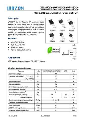
WML18 WMK18N7 8N70EM, W 70EM, WMM18N70EM WMN18 WMP18N7 8N70EM, W 70EM, WMO18N70EM 700V Super Ju MOSFET V 0.24 S unction Power M T Descrip ption WMOSTM EM is Wayon s 3rd generation super W n junction MOSFET fa that is utilizing charge M amily S balance te or extremely esistance echnology fo y low on-re S D D G G G S D G T and low ga ce. WMOSTM EM is
0.18. Size:668K way-on
wml08n70em wmk08n70em wmm08n70em wmn08n70em wmp08n70em wmo08n70em.pdf
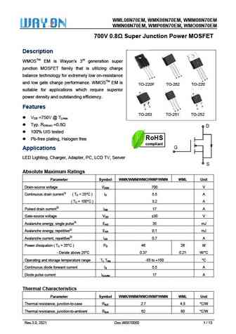
WML08 WMK08N7 8N70EM, W 70EM, WMM08N70EM WMN08 WMP08N7 8N70EM, W 70EM, WMO08N70EM 700V Power M T V 0.8 Super Junction P MOSFET Descrip ption WMOSTM EM is Wayon s 3rd generation super W n junction MOSFET fa that is utilizing charge M amily S balance te or extremely esistance echnology fo y low on-re S D D G G G S D G T and low ga ce. WMOSTM EM is at
0.19. Size:681K convert
cs8n70f.pdf
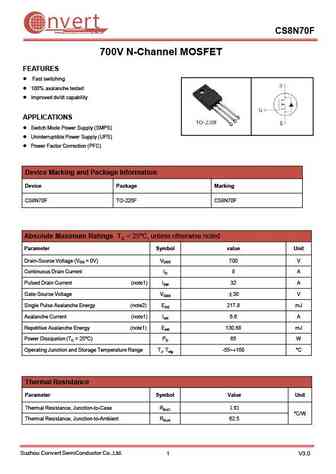
nvert Suzhou Convert Semiconductor Co ., Ltd. CS8N70F 700V N-Channel MOSFET FEATURES Fast switching 100% avalanche tested Improved dv/dt capability APPLICATIONS Switch Mode Power Supply (SMPS) Uninterruptible Power Supply (UPS) Power Factor Correction (PFC) Device Marking and Package Information Device Package Marking CS8N70F TO-220F CS8N70F Absolute Maxim
0.20. Size:410K convert
cs18n70f cs18n70v.pdf
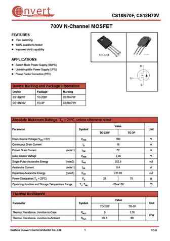
nvert Suzhou Convert Semiconductor Co ., Ltd. CS18N70F, CS18N70V 700V N-Channel MOSFET FEATURES Fast switching 100% avalanche tested Improved dv/dt capability APPLICATIONS Switch Mode Power Supply (SMPS) Uninterruptible Power Supply (UPS) Power Factor Correction (PFC) Device Marking and Package Information Device Package Marking CS18N70F TO-220F CS18N70F C
0.21. Size:3128K first semi
fir8n70fg.pdf
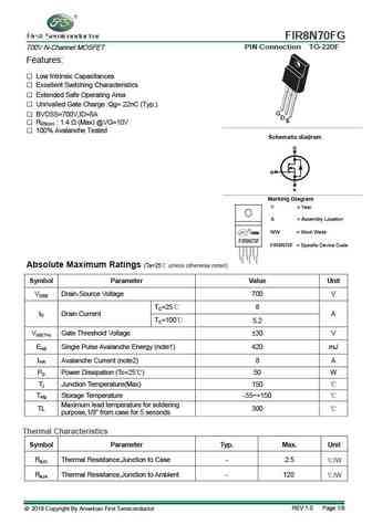
FIR8N70FG PIN Connection TO-220F 700V N-Channel MOSFET Features Low Intrinsic Capacitances Excellent Switching Characteristics Extended Safe Operating Area Unrivalled Gate Charge Qg= 22nC (Typ.) G BVDSS=700V,ID=8A D S RDS(on) 1.4 (Max) @VG=10V 100% Avalanche Tested g Schematic dia ram D G S Marking Diagram Y = Year A = Assembly Loc
0.22. Size:1089K cn hmsemi
hms8n70i hms8n70k.pdf
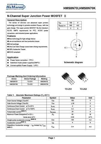
HMS8N70I,HMS8N70K N-Channel Super Junction Power MOSFET General Description The series of devices use advanced super junction V 700 V DS technology and design to provide excellent RDS(ON) with low R 540 m DS(ON) TYP. gate charge. This super junction MOSFET fits the industry s ID 8 A AC-DC SMPS requirements for PFC, AC/DC power conversion, and industrial power applic
0.23. Size:965K cn hmsemi
hms8n70d hms8n70 hms8n70f.pdf
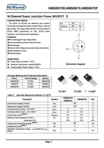
HMS8N70D,HMS8N70,HMS8N70F N-Channel Super Junction Power MOSFET General Description The series of devices use advanced super junction VDS 700 V technology and design to provide excellent RDS(ON) with low RDS(ON) TYP. 540 m gate charge. This super junction MOSFET fits the industry s ID 8 A AC-DC SMPS requirements for PFC, AC/DC power conversion, and industrial power app
Otros transistores... 3N70
, 3N70A
, 3N70K
, 4N70
, 4N70K
, 5N70K
, 6N70
, 7N70
, AON6380
, 9N70
, 10N70
, 12N70
, 15N70
, 6N65Z
, 7N65A
, 7N65
, 7N65Z
.