10N65 Datasheet. Equivalente. Reemplazo. Hoja de especificaciones. Principales características
Número de Parte: 10N65 📄📄
Tipo de FET: MOSFET
Polaridad de transistor: N
ESPECIFICACIONES MÁXIMAS
Pdⓘ - Máxima disipación de potencia: 178 W
|Vds|ⓘ - Voltaje máximo drenador-fuente: 650 V
|Vgs|ⓘ - Voltaje máximo fuente-puerta: 30 V
|Id|ⓘ - Corriente continua de drenaje: 10 A
Tjⓘ - Temperatura máxima de unión: 150 °C
CARACTERÍSTICAS ELÉCTRICAS
trⓘ - Tiempo de subida: 69 nS
Cossⓘ - Capacitancia de salida: 166 pF
RDSonⓘ - Resistencia estado encendido drenaje a fuente: 0.72 Ohm
Encapsulados: TO-263 TO-220 TO-262 TO-220F TO-220F1 TO-220F2
📄📄 Copiar
Búsqueda de reemplazo de 10N65 MOSFET
- Selecciónⓘ de transistores por parámetros
10N65 datasheet
10n65.pdf
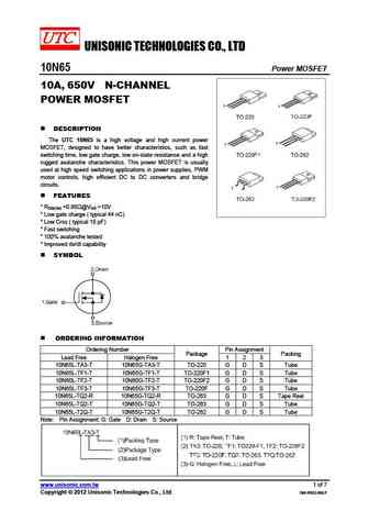
UNISONIC TECHNOLOGIES CO., LTD 10N65 Power MOSFET 10A, 650V N-CHANNEL POWER MOSFET DESCRIPTION The UTC 10N65 is a high voltage and high current power MOSFET, designed to have better characteristics, such as fast switching time, low gate charge, low on-state resistance and a high rugged avalanche characteristics. This power MOSFET is usually used at high speed switching appli
10n65.pdf
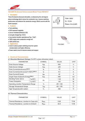
10N65 10A 650V N-channel Enhancement Mode Power MOSFET 1 Description These N-channel enhanced vdmosfets, is obtained by the self-aligned V DSS = 650V planar technology which reduce the conduction loss, improve switching I = 10.0A D performance and enhance the avalanche energy. Which accords with the RoHS standard. R DS(on) TYP) =0.86 2 Features Fast switching ESD imp
10n65.pdf
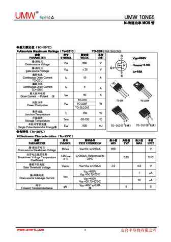
R UMW UMW 10N65 UMW 10N65 N- MOS N- MOS N- MOS N- MOS TC=25 C TC=25 C TC=25 C TC=25 C Absolute Maximum Ratings Tc=25 C TO-220 Absolute Maximum Ratings Tc=25 C TO-220 Absolute Maximum Ratings Tc=25 C TO-220 Absolute Maximum Ratings Tc=25 C TO-220/220F/262/263 PARAMETER
svf10n65f svf10n65t.pdf
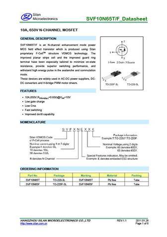
SVF10N65T/F_Datasheet 10A, 650V N-CHANNEL MOSFET GENERAL DESCRIPTION SVF10N65T/F is an N-channel enhancement mode power MOS field effect transistor which is produced using Silan proprietary F-CellTM structure VDMOS technology. The improved planar stripe cell and the improved guard ring terminal have been especially tailored to minimize on-state resistance, provide superior switch
stl10n65m2.pdf
STL10N65M2 Datasheet N-channel 650 V, 0.85 typ., 4.5 A MDmesh M2 Power MOSFET in a PowerFLAT 5x6 HV package Features VDS RDS(on ) max. ID Order code STL10N65M2 650 V 1.00 4.5 A 1 2 Extremely low gate charge 3 4 Excellent output capacitance (COSS) profile PowerFLAT 5x6 HV 100% avalanche tested Zener-protected D(5, 6, 7, 8) 8 7 6 5 Applications Switch

fcp110n65f.pdf
August 2014 FCP110N65F N-Channel SuperFET II FRFET MOSFET 650 V, 35 A, 110 m Features Description 700 V @ TJ = 150 C SuperFET II MOSFET is Fairchild Semiconductor s brand-new high voltage super-junction (SJ) MOSFET family that is utilizing Typ. RDS(on) = 96 m (Typ.) charge balance technology for outstanding low on-resistance Ultra Low Gate Charge (Typ. Qg = 98
fch110n65f.pdf
December 2014 FCH110N65F N-Channel SuperFET II FRFET MOSFET 650 V, 35 A, 110 m Features Description 700 V @ TJ = 150 C SuperFET II MOSFET is Fairchild Semiconductor s brand-new high voltage super-junction (SJ) MOSFET family that is utilizing Typ. RDS(on) = 96 m (Typ.) charge balance technology for outstanding low on-resistance Ultra Low Gate Charge (Typ. Qg
fcb110n65f.pdf
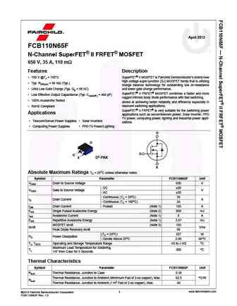
April 2015 FCB110N65F N-Channel SuperFET II FRFET MOSFET 650 V, 35 A, 110 m Features Description 700 V @TJ = 150 C SuperFET II MOSFET is Fairchild Semiconductor s brand-new high voltage super-junction (SJ) MOSFET family that is utilizing Typ. RDS(on) = 96 m (Typ.) charge balance technology for outstanding low on-resistance Ultra Low Gate Charge (Typ. Qg = 98 nC
ika10n65et6.pdf
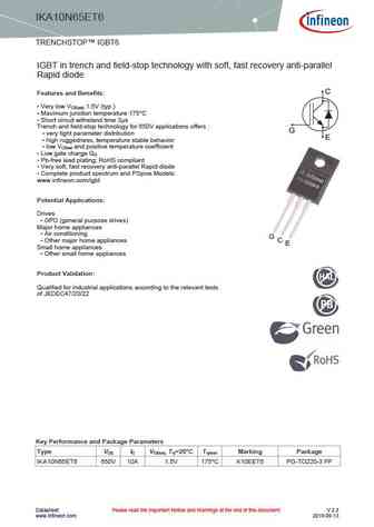
IKA10N65ET6 TRENCHSTOP IGBT6 IGBT in trench and field-stop technology with soft, fast recovery anti-parallel Rapid diode C Features and Benefits Very low V 1.5V (typ.) CE(sat) Maximum junction temperature 175 C Short circuit withstand time 3 s Trench and field-stop technology for 650V applications offers G very tight parameter distribution E high rugg
ixxr110n65b4h1.pdf
VCES = 650V XPTTM 650V GenX4TM IXXR110N65B4H1 IC110 = 70A w/ Sonic Diode VCE(sat) 2.20V (Electrically Isolated Tab) tfi(typ) = 85ns Extreme Light Punch Through IGBT for 10-30kHz Switching ISOPLUS247TM Symbol Test Conditions Maximum Ratings VCES TJ = 25 C to 175 C 650 V VCGR TJ = 25 C to 175 C, RGE = 1M 650 V G C VGES Continuous 20 V Isolated Ta
ixyp10n65c3d1.pdf
Preliminary Technical Information XPTTM 650V IGBT VCES = 650V IXYP10N65C3D1 GenX3TM w/Diode IC110 = 9A VCE(sat) 2.50V tfi(typ) = 23ns Extreme Light Punch Through IGBT for 20-60kHz Switching TO-220 Symbol Test Conditions Maximum Ratings G VCES TJ = 25 C to 175 C 650 V C Tab E VCGR TJ = 25 C to 175 C, RGE
ixyp10n65c3d1m.pdf
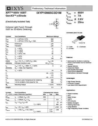
Preliminary Technical Information XPTTM 650V IGBT VCES = 650V IXYP10N65C3D1M GenX3TM w/Diode IC110 = 7A VCE(sat) 2.6V (Electrically Isolated Tab) tfi(typ) = 23ns Extreme Light Punch Through IGBT for 20-60kHz Switching OVERMOLDED TO-220 Symbol Test Conditions Maximum Ratings VCES TJ = 25 C to 175 C 650 V VCGR
ixxh110n65c4.pdf
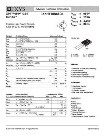
Advance Technical Information XPTTM 650V IGBT VCES = 650V IXXH110N65C4 GenX4TM IC110 = 110A VCE(sat) 2.35V Extreme Light Punch Through tfi(typ) = 30ns IGBT for 20-60 kHz Switching Symbol Test Conditions Maximum Ratings TO-247 AD VCES TJ = 25 C to 175 C 650 V VCGR TJ = 25 C to 175 C, RGE = 1M 650 V VGES Continuous 20 V VGEM Transient 30 V G C
ixxn110n65c4h1.pdf
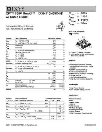
VCES = 650V XPTTM 650V GenX4TM IXXN110N65C4H1 IC110 = 110A w/ Sonic Diode VCE(sat) 2.35V tfi(typ) = 30ns Extreme Light Punch Through IGBT for 20-60kHz Switching E SOT-227B, miniBLOC E153432 E Symbol Test Conditions Maximum Ratings G VCES TJ = 25 C to 175 C 650 V VCGR TJ = 25 C to 175 C, RGE = 1M
ixxn110n65b4h1.pdf
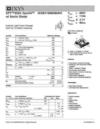
VCES = 650V XPTTM 650V GenX4TM IXXN110N65B4H1 IC110 = 110A w/ Sonic Diode VCE(sat) 2.1V tfi(typ) = 85ns Extreme Light Punch Through IGBT for 10-30kHz Switching E SOT-227B, miniBLOC E153432 Symbol Test Conditions Maximum Ratings E VCES TJ = 25 C to 175 C 650 V G VCGR TJ = 25 C to 175 C, RGE = 1M 6
ixxk110n65b4h1.pdf
VCES = 650V XPTTM 650V GenX4TM IXXK110N65B4H1 IC110 = 110A w/ Sonic Diode IXXX110N65B4H1 VCE(sat) 2.1V tfi(typ) = 85ns Extreme Light Punch Through IGBT for 10-30kHz Switching TO-264 (IXXK) Symbol Test Conditions Maximum Ratings G C VCES TJ = 25 C to 175 C 650 V E VCGR TJ = 25 C to 175 C, RGE = 1M 650 V Tab VGES Continuous 20 V PLUS247 (IXXX)
ixxx110n65b4h1.pdf

VCES = 650V XPTTM 650V GenX4TM IXXK110N65B4H1 IC110 = 110A w/ Sonic Diode IXXX110N65B4H1 VCE(sat) 2.1V tfi(typ) = 85ns Extreme Light Punch Through IGBT for 10-30kHz Switching TO-264 (IXXK) Symbol Test Conditions Maximum Ratings G C VCES TJ = 25 C to 175 C 650 V E VCGR TJ = 25 C to 175 C, RGE = 1M 650 V Tab VGES Continuous 20 V PLUS247 (IXXX)
ixyp10n65c3.pdf
Preliminary Technical Information XPTTM 650V IGBT VCES = 650V IXYP10N65C3 GenX3TM IC110 = 10A VCE(sat) 2.50V tfi(typ) = 23ns Extreme Light Punch Through IGBT for 20-60kHz Switching TO-220 Symbol Test Conditions Maximum Ratings VCES TJ = 25 C to 175 C 650 V VCGR TJ = 25 C to 175 C, RGE = 1M 650 V G C Ta
fcp110n65f.pdf

Is Now Part of To learn more about ON Semiconductor, please visit our website at www.onsemi.com Please note As part of the Fairchild Semiconductor integration, some of the Fairchild orderable part numbers will need to change in order to meet ON Semiconductor s system requirements. Since the ON Semiconductor product management systems do not have the ability to manage part nomenclatur
fch110n65f.pdf
FCH110N65F N-Channel SuperFET II FRFET MOSFET 650 V, 35 A, 110 m Features Description 700 V @ TJ = 150 C SuperFET II MOSFET is ON Semiconductor s brand-new high voltage super-junction (SJ) MOSFET family that is utilizing Typ. RDS(on) = 96 m (Typ.) charge balance technology for outstanding low on-resistance Ultra Low Gate Charge (Typ. Qg = 98 nC) and lower g
fcb110n65f.pdf

Is Now Part of To learn more about ON Semiconductor, please visit our website at www.onsemi.com Please note As part of the Fairchild Semiconductor integration, some of the Fairchild orderable part numbers will need to change in order to meet ON Semiconductor s system requirements. Since the ON Semiconductor product management systems do not have the ability to manage part nomenclatur
ntb110n65s3hf.pdf
NTB110N65S3HF MOSFET N Channel, SUPERFET III, FRFET 650 V, 30 A, 110 mW Description www.onsemi.com SUPERFET III MOSFET is ON Semiconductor s brand-new high voltage super-junction (SJ) MOSFET family that is utilizing charge balance technology for outstanding low on-resistance and lower gate charge performance. This advanced technology is tailored to minimize VDSS RDS(ON) MAX ID
nthl110n65s3f.pdf
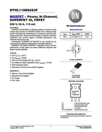
NTHL110N65S3F MOSFET Power, N-Channel, SUPERFET III, FRFET 650 V, 30 A, 110 mW Description www.onsemi.com SUPERFET III MOSFET is ON Semiconductor s brand-new high voltage super-junction (SJ) MOSFET family that is utilizing charge balance technology for outstanding low on-resistance and lower gate VDSS RDS(on) MAX ID MAX charge performance. This advanced technology is tailored to
nvb110n65s3f.pdf
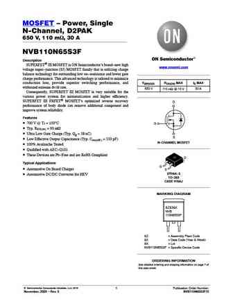
MOSFET Power, Single N-Channel, D2PAK 650 V, 110 mW, 30 A NVB110N65S3F Description SUPERFET III MOSFET is ON Semiconductor s brand-new high www.onsemi.com voltage super-junction (SJ) MOSFET family that is utilizing charge balance technology for outstanding low on-resistance and lower gate charge performance. This advanced technology is tailored to minimize V(BR)DSS RDS(ON) MAX
ntpf110n65s3hf.pdf
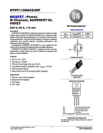
NTPF110N65S3HF MOSFET Power, N-Channel, SUPERFET III, FRFET 650 V, 30 A, 110 mW www.onsemi.com Description SUPERFET III MOSFET is ON Semiconductor s brand-new high VDSS RDS(ON) MAX ID MAX voltage super-junction (SJ) MOSFET family that is utilizing charge 650 V 110 mW @ 10 V 30 A balance technology for outstanding low on-resistance and lower gate charge performance. This advance
ntp110n65s3hf.pdf
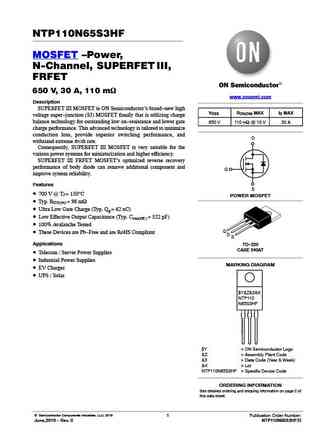
NTP110N65S3HF MOSFET Power, N-Channel, SUPERFET III, FRFET 650 V, 30 A, 110 mW www.onsemi.com Description SUPERFET III MOSFET is ON Semiconductor s brand-new high VDSS RDS(ON) MAX ID MAX voltage super-junction (SJ) MOSFET family that is utilizing charge balance technology for outstanding low on-resistance and lower gate 650 V 110 mW @ 10 V 30 A charge performance. This advanced
10n65kl-ta3-t 10n65kg-ta3-t 10n65kl-tf1-t 10n65kg-tf1-t 10n65kl-tf2-t 10n65kg-tf2-t.pdf
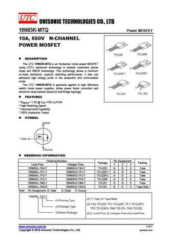
UNISONIC TECHNOLOGIES CO., LTD 10N65K-MTQ Power MOSFET 10A, 650V N-CHANNEL POWER MOSFET DESCRIPTION The UTC 10N65K-MTQ is an N-channel mode power MOSFET using UTC s advanced technology to provide customers planar stripe and DMOS technology. This technology allows a minimum on-state resistance, superior switching performance. It also can withstand high energy pulse in the
10n65k.pdf
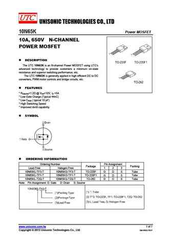
UNISONIC TECHNOLOGIES CO., LTD 10N65K Power MOSFET 10A, 650V N-CHANNEL POWER MOSFET DESCRIPTION The UTC 10N65K is an N-channel Power MOSFET using UTC s advanced technology to provide customers a minimum on-state resistance and superior switching performance, etc. The UTC 10N65K is generally applied in high efficient DC to DC converters, PWM motor controls and bridge cir
10n65kl-ta3-t 10n65kg-ta3-t 10n65kl-tf3-t 10n65kg-tf3-t 10n65kl-tf1-t 10n65kg-tf1-t 10n65kl-tf2-t 10n65kg-tf2-t 10n65kl-t2q-t 10n65kg-t2q-t.pdf
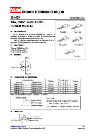
UNISONIC TECHNOLOGIES CO., LTD 10N65K Power MOSFET 10A, 650V N-CHANNEL POWER MOSFET DESCRIPTION The UTC 10N65K is an N-channel Power MOSFET using UTC s advanced technology to provide customers a minimum on-state resistance and superior switching performance, etc. The UTC 10N65K is generally applied in high efficient DC to DC converters, PWM motor controls and bridge cir
10n65z.pdf
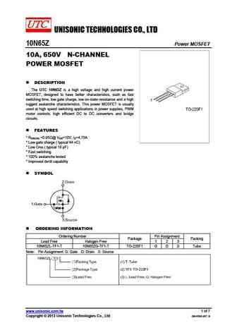
UNISONIC TECHNOLOGIES CO., LTD 10N65Z Power MOSFET 10A, 650V N-CHANNEL POWER MOSFET DESCRIPTION The UTC 10N65Z is a high voltage and high current power MOSFET, designed to have better characteristics, such as fast switching time, low gate charge, low on-state resistance and a high rugged avalanche characteristics. This power MOSFET is usually used at high speed switching a
10n65kl-tf3-t 10n65kg-tf3-t 10n65kl-tm3-t 10n65kg-tm3-t 10n65kl-tn3-r 10n65kg-tn3-r.pdf

UNISONIC TECHNOLOGIES CO., LTD 10N65K-MTQ Power MOSFET 10A, 650V N-CHANNEL POWER MOSFET DESCRIPTION The UTC 10N65K-MTQ is an N-channel mode power MOSFET using UTC s advanced technology to provide customers planar stripe and DMOS technology. This technology allows a minimum on-state resistance, superior switching performance. It also can withstand high energy pulse in the
cjpf10n65.pdf
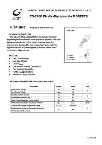
JIANGSU CHANGJIANG ELECTRONICS TECHNOLOGY CO., LTD TO-220F Plastic-Encapsulate MOSFETS CJPF10N65 N-Channel Power MOSFET TO-220F GENERAL DESCRIPTION This advanced high voltage MOSFET is designed to stand high energy in the avalanche mode and switch efficiently. This new high energy device also offers a drain-to-source diode fast recovery time. Designed for high voltage, high s
cjp10n65.pdf
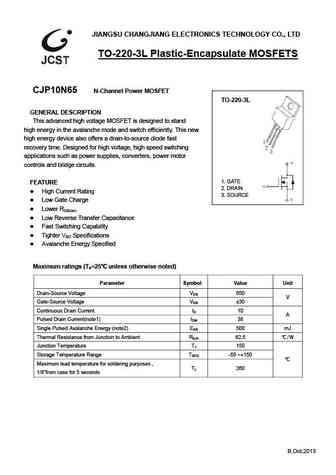
JIANGSU CHANGJIANG ELECTRONICS TECHNOLOGY CO., LTD TO-220-3L Plastic-Encapsulate MOSFETS CJP10N65 N-Channel Power MOSFET TO-220-3L GENERAL DESCRIPTION This advanced high voltage MOSFET is designed to stand high energy in the avalanche mode and switch efficiently. This new high energy device also offers a drain-to-source diode fast recovery time. Designed for high voltage, hig
kf10n65f.pdf
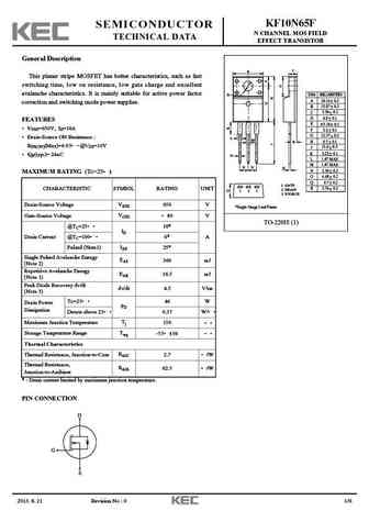
KF10N65F SEMICONDUCTOR N CHANNEL MOS FIELD TECHNICAL DATA EFFECT TRANSISTOR General Description C A This planar stripe MOSFET has better characteristics, such as fast switching time, low on resistance, low gate charge and excellent avalanche characteristics. It is mainly suitable for active power factor E DIM MILLIMETERS _ A 10.16 0.2 + correction and switching mode power suppli
cep10n65 ceb10n65 cef10n65.pdf
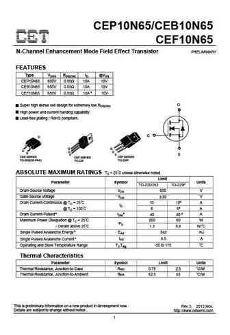
CEP10N65/CEB10N65 CEF10N65 N-Channel Enhancement Mode Field Effect Transistor PRELIMINARY FEATURES Type VDSS RDS(ON) ID @VGS CEP10N65 650V 0.85 10A 10V CEB10N65 650V 0.85 10A 10V CEF10N65 650V 0.85 10A d 10V D Super high dense cell design for extremely low RDS(ON). High power and current handing capability. Lead-free plating ; RoHS compliant. G S CEB SERIES CEP SERIES CE
h10n65.pdf
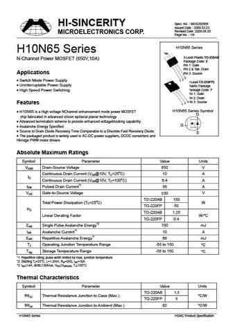
Spec. No. MOS200906 HI-SINCERITY Issued Date 2009.03.23 Revised Date 2009.08.05 MICROELECTRONICS CORP. Page No. 1/6 H10N65 Series H10N65 Series Tab 3-Lead Plastic TO-220AB N-Channel Power MOSFET (650V,10A) Package Code E Pin 1 Gate Pin 2 & Tab Drain Applications Pin 3 Source 3 2 Switch Mode Power Supply 1 3-Lead TO-220FP) Uninterruptable P
aowf10n65.pdf

AOW10N65/AOWF10N65 650V,10A N-Channel MOSFET General Description Product Summary VDS 750V@150 The AOW10N65/AOWF10N65 is fabricated using an advanced high voltage MOSFET process that is designed ID (at VGS=10V) 10A to deliver high levels of performance and robustness in RDS(ON) (at VGS=10V)
aot10n65.pdf

AOT10N65/AOTF10N65 650V,10A N-Channel MOSFET General Description Product Summary VDS 750V@150 The AOT10N65 & AOTF10N65 have been fabricated using an advanced high voltage MOSFET process that is ID (at VGS=10V) 10A designed to deliver high levels of performance and RDS(ON) (at VGS=10V)
aotf10n65.pdf
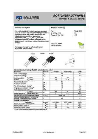
AOT10N65/AOTF10N65 650V,10A N-Channel MOSFET General Description Product Summary VDS 750V@150 The AOT10N65 & AOTF10N65 have been fabricated using an advanced high voltage MOSFET process that is ID (at VGS=10V) 10A designed to deliver high levels of performance and RDS(ON) (at VGS=10V)
aow10n65.pdf
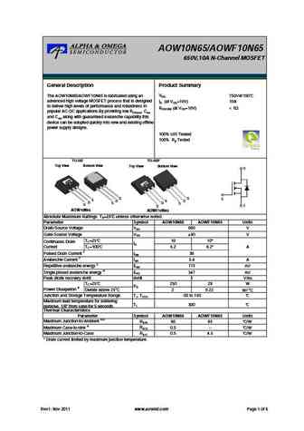
AOW10N65/AOWF10N65 650V,10A N-Channel MOSFET General Description Product Summary VDS 750V@150 The AOW10N65/AOWF10N65 is fabricated using an advanced high voltage MOSFET process that is designed ID (at VGS=10V) 10A to deliver high levels of performance and robustness in RDS(ON) (at VGS=10V)
afn10n65t220ft afn10n65t220t.pdf
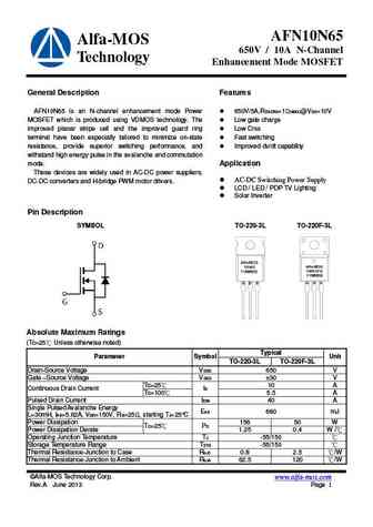
AFN10N65 Alfa-MOS 650V / 10A N-Channel Technology Enhancement Mode MOSFET General Description Features AFN10N65 is an N-channel enhancement mode Power 650V/5A,RDS(ON)=1 (MAX)@VGS=10V MOSFET which is produced using VDMOS technology. The Low gate charge improved planar stripe cell and the improved guard ring Low Crss terminal have been especially tailored to minimize on-state
sif10n65c.pdf
Shenzhen SI Semiconductors Co., LTD. Product Specification Shenzhen SI Semiconductors Co., LTD. Product Specification Shenzhen SI Semiconductors Co., LTD. Product Specification Shenzhen SI Semiconductors Co., LTD. Product Specification N- MOS / N-CHANNEL POWER MOSFET SIF10N65C N- MOS / N-CHANNEL POWER MOSFET SIF10N65C
jcs10n65bt jcs10n65st jcs10n65ct jcs10n65ft.pdf
N R N-CHANNEL MOSFET JCS10N65T MAIN CHARACTERISTICS Package ID 9.5 A VDSS 650 V Rdson-max 0.95 @Vgs=10V Qg-typ 34 nC APPLICATIONS High frequency switching mode power supply Electronic ballast UPS UPS FEATURE
jcs10n65f jcs10n65c jcs10n65b jcs10n65s.pdf
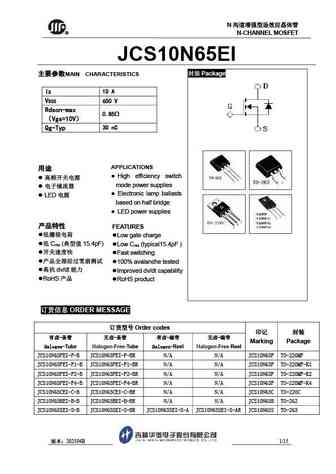
N R N-CHANNEL MOSFET JCS10N65EI Package MAIN CHARACTERISTICS ID 10 A VDSS 650 V Rdson-max 0.85 Vgs=10V Qg-Typ 30 nC APPLICATIONS High efficiency switch mode power supplies Electronic lamp ballasts LED based on half bridge
mtn10n65ea.pdf
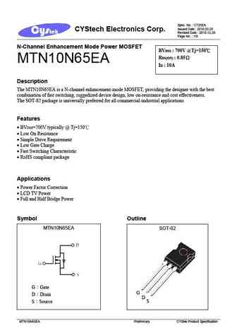
Spec. No. C725EA Issued Date 2010.02.25 CYStech Electronics Corp. Revised Date 2010.12.29 Page No. 1/9 N-Channel Enhancement Mode Power MOSFET BVDSS 700V @Tj=150 RDS(ON) 0.85 MTN10N65EA ID 10A Description The MTN10N65EA is a N-channel enhancement-mode MOSFET, providing the designer with the best combination of fast switching, ruggedized device design, l
mtn10n65fpg.pdf
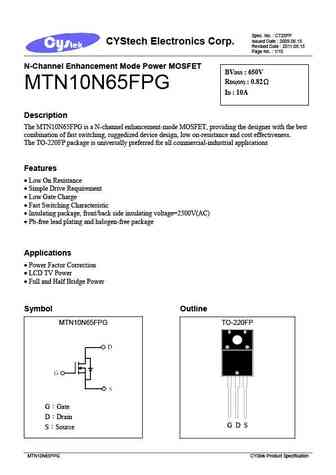
Spec. No. C725FP Issued Date 2009.06.15 CYStech Electronics Corp. Revised Date 2011.08.15 Page No. 1/10 N-Channel Enhancement Mode Power MOSFET BVDSS 650V RDS(ON) 0.82 MTN10N65FPG ID 10A Description The MTN10N65FPG is a N-channel enhancement-mode MOSFET, providing the designer with the best combination of fast switching, ruggedized device design, low on-re
mtn10n65fp.pdf
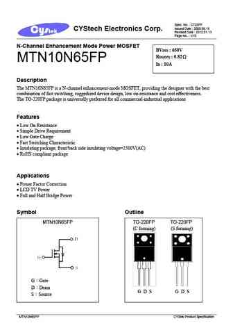
Spec. No. C725FP Issued Date 2009.06.15 CYStech Electronics Corp. Revised Date 2012.01.13 Page No. 1/10 N-Channel Enhancement Mode Power MOSFET BVDSS 650V RDS(ON) 0.82 MTN10N65FP ID 10A Description The MTN10N65FP is a N-channel enhancement-mode MOSFET, providing the designer with the best combination of fast switching, ruggedized device design, low on-resi
10n65a 10n65af.pdf
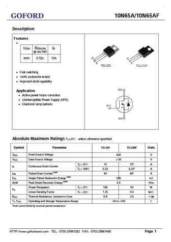
10N65A/10N65AF GOFORD Description Features VDSS RDS(ON) ID @ 10V (typ) 10A 650V 0.72 Fast switching 100% avalanche tested Improved dv/dt capability Application Active power factor correction Uninterruptible Power Supply (UPS) Electronic lamp ballasts Absolute Maximum Ratings TC=25 unless otherwise specified Symbol Parameter TO-220
brfl10n65.pdf
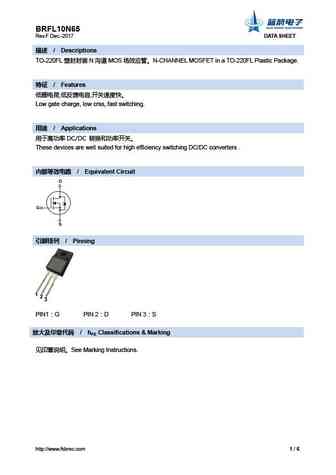
BRFL10N65 Rev.F Dec.-2017 DATA SHEET / Descriptions TO-220FL N MOS N-CHANNEL MOSFET in a TO-220FL Plastic Package. / Features , , Low gate charge, low crss, fast switching. / Applications DC/DC These devices are well suited for high effi
brf10n65.pdf
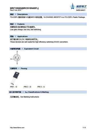
BRF10N65(BRCS10N65FL) Rev.C Feb.-2015 DATA SHEET / Descriptions TO-220FL N MOS N-CHANNEL MOSFET in a TO-220FL Plastic Package. / Features , , Low gate charge, low crss, fast switching. / Applications DC/DC These devices are well suited f
brfl10n65s.pdf
BRFL10N65S Rev.A Dec.-2023 DATA SHEET / Descriptions TO-220FL N MOS N-CHANNEL MOSFET in a TO-220FL Plastic Package. / Features Low gate charge, low crss, fast switching,Have good Electromagnetic Interference porformance. / Applications
brb10n65.pdf
BRB10N65 Rev.E Sep.-2022 DATA SHEET / Descriptions TO-263 N MOS N-CHANNEL MOSFET in a TO-263 Plastic Package. / Features , , , Low gate charge, low crss, fast switching, HF product. / Applications DC/DC These devices are well
bra10n65.pdf
BRA10N65 Rev.B Sep.-2022 DATA SHEET / Descriptions TO-262 N MOS N-CHANNEL MOSFET in a TO-262 Plastic Package. / Features , , , Low gate charge, low crss, fast switching, HF product. / Applications DC/DC These devices are well
cs10n65 a8hd.pdf

Silicon N-Channel Power MOSFET R CS10N65 A8HD VDSS 650 V General Description ID 10 A CS10N65 A8HD, the silicon N-channel Enhanced PD (TC=25 ) 130 W VDMOSFETs, is obtained by the self-aligned planar RDS(ON)Typ 0.65 Technology which reduce the conduction loss, improve switching performance and enhance the avalanche energy. The transistor can be used in various
cs10n65f a9r.pdf

Silicon N-Channel Power MOSFET R CS10N65F A9R General Description VDSS 650 V CS10N65F A9R, the silicon N-channel Enhanced ID 10 A PD(TC=25 ) 40 W VDMOSFETs, is obtained by the self-aligned planar Technology RDS(ON)Typ 0.86 which reduce the conduction loss, improve switching performance and enhance the avalanche energy. The transistor can be used in various p
cs10n65f a9hd.pdf
Silicon N-Channel Power MOSFET R CS10N65F A9HD VDSS 650 V General Description ID 10 A CS10N65F A9HD, the silicon N-channel Enhanced PD (TC=25 ) 50 W VDMOSFETs, is obtained by the self-aligned planar RDS(ON)Typ 0.65 Technology which reduce the conduction loss, improve switching performance and enhance the avalanche energy. The transistor can be used in vario
cs10n65 a8r.pdf
Silicon N-Channel Power MOSFET R CS10N65 A8R General Description VDSS 650 V CS10N65 A8R, the silicon N-channel Enhanced ID 10 A PD(TC=25 ) 130 W VDMOSFETs, is obtained by the self-aligned planar Technology RDS(ON)Typ 0.86 which reduce the conduction loss, improve switching performance and enhance the avalanche energy. The transistor can be used in various po
cm10n65az.pdf
R CM10N65AZ www.jdsemi.cn ShenZhen Jingdao Electronic Co.,Ltd. POWER MOSFET 650V N-Channel VDMOS RoHS 1 LD E 2
ftk10n65p f dd.pdf
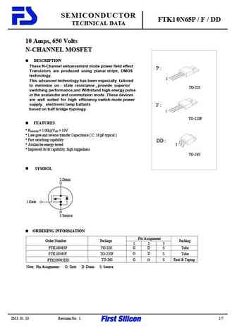
SEMICONDUCTOR FTK10N65P / F / DD TECHNICAL DATA 10 Amps, 650 Volts N-CHANNEL MOSFET DESCRIPTION These N-Channel enhancement mode power field effect P Transistors are produced using planar stripe, DMOS technology. 1 This advanced technology has been especially tailored to minimize on - state resistance , provide superior TO-220 switching performance,and Withstand high energy pul
f10n65.pdf
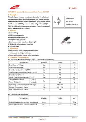
F10N65 10A 650V N-channel Enhancement Mode Power MOSFET 1 Description These N-channel enhanced vdmosfets, is obtained by the self-aligned V DSS = 650V planar technology which reduce the conduction loss, improve switching I = 10.0A D performance and enhance the avalanche energy. Which accords with the RoHS standard. TO-220F provides insulation voltage rated at 2000V R DS(on) TYP)
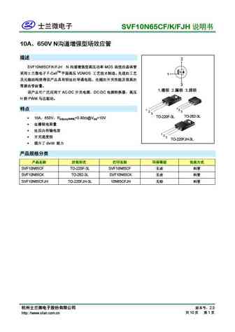
svf10n65t svf10n65f svf10n65k svf10n65s svf10n65str.pdf
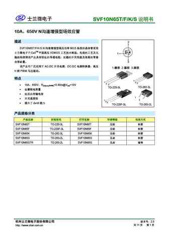
SVF10N65T/F/K/S 10A 650V N 2 SVF10N65T/F/K/S N MOS F-CellTM VDMOS 1 3
svf10n65cfj.pdf
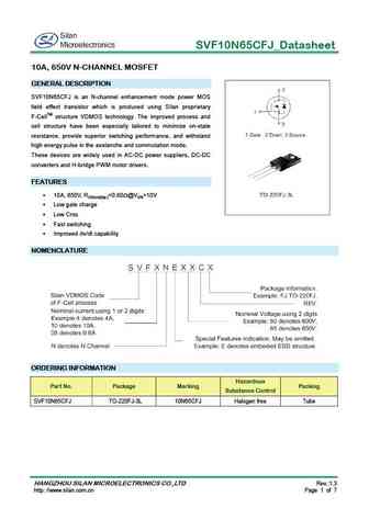
SVF10N65CFJ_Datasheet 10A, 650V N-CHANNEL MOSFET GENERAL DESCRIPTION SVF10N65CFJ is an N-channel enhancement mode power MOS field effect transistor which is produced using Silan proprietary F-CellTM structure VDMOS technology. The improved process and cell structure have been especially tailored to minimize on-state resistance, provide superior switching performance, and withstand
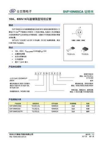
svf10n65cf svf10n65ck svf10n65cfjh.pdf
SVF10N65CF/K/FJH 10A 650V N 2 SVF10N65CF/K/FJH N MOS F-CellTM VDMOS 1 3 1. 2.
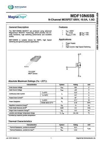
mdf10n65bth.pdf
MDF10N65B N-Channel MOSFET 650V, 10.0A, 1.0 General Description Features The MDF10N65B MOSFET are produced using advanced V = 650V DS MagnaChip s MOSFET Technology, which provides low on- I = 10.0A @ V = 10V D GS state resistance, high switching performance and excellent R 1.0 @ V = 10V DS(ON) GS quality. Applications MDF10N65B is suitable device for
msf10n65.pdf
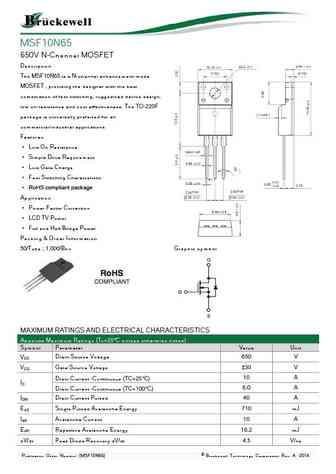
MSF10N65 650V N-Channel MOSFET Description The MSF10N65 is a N-channel enhancement-mode MOSFET , providing the designer with the best combination of fast switching, ruggedized device design, low on-resistance and cost effectiveness. The TO-220F package is universally preferred for all commercial-industrial applications Features Low On Resistance Simple Drive Requir
ms10n65.pdf
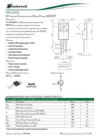
MS10N65 N-Channel Enhancement Mode Power MOSFET Description The MS10N65 is a N-channel enhancement-mode MOSFET, providing the designer with the best combination of fast switching, ruggedized device design, low on-resistance and cost effectiveness. The TO-220 package is universally preferred for all commercial-industrial applications Features BVDSS=700V typically @ Tj=150
wfp10n65.pdf
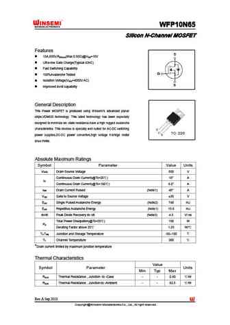
WFP10N65 WFP10N65 WFP10N65 WFP10N65 Silicon N-Channel MOSFET Silicon N-Channel MOSFET Silicon N-Channel MOSFET Silicon N-Channel MOSFET Features 10A,650V,R (Max 0.95 )@V =10V DS(on) GS Ultra-low Gate Charge(Typical 43nC) Fast Switching Capability 100%Avalanche Tested Isolation Voltage(V =4000V AC) ISO Improved dv/dt capability General Description This
wff10n65.pdf
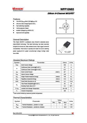
WFF10N65 WFF10N65 WFF10N65 WFF10N65 Silicon N-Channel MOSFET Silicon N-Channel MOSFET Silicon N-Channel MOSFET Silicon N-Channel MOSFET Features 10A,650V,R (Max 0.95 )@V =10V DS(on) GS Ultra-low Gate Charge(Typical 43nC) Fast Switching Capability 100%Avalanche Tested Isolation Voltage(V =4000V AC) ISO Improved dv/dt capability General Description This
bl10n65a-p bl10n65a-a.pdf
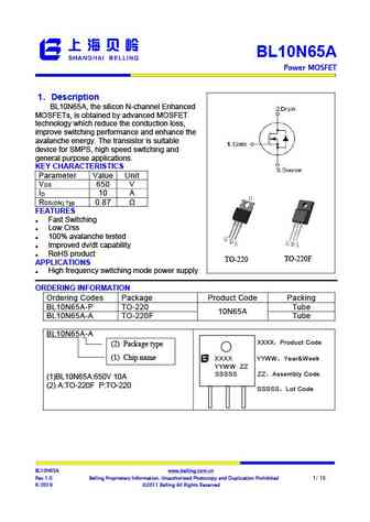
BL10N65A Power MOSFET 1 Description Step-Down Converter BL10N65A, the silicon N-channel Enhanced , MOSFETs, is obtained by advanced MOSFET technology which reduce the conduction loss, improve switching performance and enhance the avalanche energy. The transistor is suitable device for SMPS, high speed switching and general purpose applications. KEY CHARACTERISTICS
fhp10n65b fhf10n65b.pdf

N N-CHANNEL MOSFET FHP10N65B/FHF10N65B MAIN CHARACTERISTICS FEATURES Low gate charge ID 10A Crss ( 18pF) Low Crss (typical 18pF ) VDSS 650V Fast switching Rdson-typ 0.75 @Vgs=10V 100% 100% avalanche tested Qg-typ 30nC dv/dt
fhp10n65a fhf10n65a.pdf
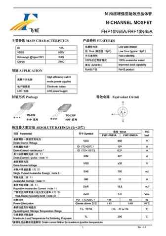
N N-CHANNEL MOSFET FHP10N65A/FHF10N65A MAIN CHARACTERISTICS FEATURES Low gate charge ID 10A Crss ( 18pF) Low Crss (typical 18pF ) VDSS 650V Fast switching Rdson-typ 0.8 @Vgs=10V 100% 100% avalanche tested Qg-typ 29nC dv/dt Improved dv/dt capability RoHS RoHS product APPLICATION High efficiency switch mode pow
hy10n65t.pdf
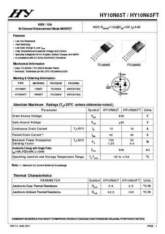
HY10N65T / HY10N65FT 650V / 10A 650V, RDS(ON)=1.0 @VGS=10V, ID=5.0A N-Channel Enhancement Mode MOSFET Features Low ON Resistance Fast Switching Low Gate Charge & Low CRSS Fully Characterized Avalanche Voltage and Current Specially Desigened for AC Adapter, Battery Charger and SMPS 1 1 2 2 In compliance with EU RoHs 2002/95/EC Directives G G 3 3 D D S
jfpc10n65ci.pdf
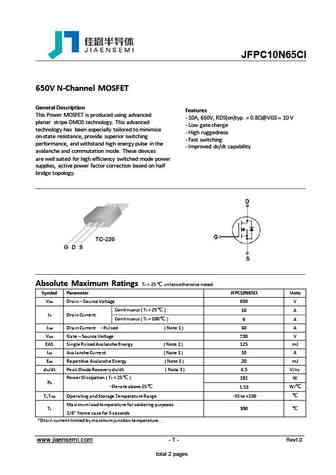
JFPC10N65CI 650V N-Channel MOSFET General Description Features This Power MOSFET is produced using advanced - 10A, 650V, RDS(on)typ. = 0.8 @VGS = 10 V planar stripe DMOS technology. This advanced - Low gate charge technology has been especially tailored to minimize - High ruggedness on-state resistance, provide superior switching - Fast switching performance, and withst
jfpc10n65d.pdf
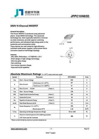
JFPC10N65D 650V N-Channel MOSFET General Description This Power MOSFET is produced using advanced planar stripe DMOS technology. This advanced technology has been especially tailored to minimize on-state resistance, provide superior switching performance, and withstand high energy pulse in the avalanche and commutation mode. These devices are well suited for high efficiency
jffc10n65d.pdf
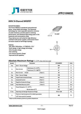
JFFC10N65D 650V N-Channel MOSFET General Description This Power MOSFET is produced using advanced planar stripe DMOS technology. This advanced technology has been especially tailored to minimize on-state resistance, provide superior switching performance, and withstand high energy pulse in the avalanche and commutation mode. These devices are well suited for high efficiency
jfpc10n65c jffc10n65c.pdf
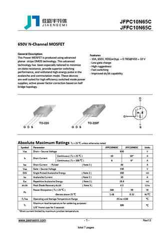
JFPC10N65C JFFC10N65C 650V N-Channel MOSFET General Description Features This Power MOSFET is produced using advanced - 10A, 650V, RDS(on)typ. = 0.78 @VGS = 10 V planar stripe DMOS technology. This advanced - Low gate charge technology has been especially tailored to minimize - High ruggedness on-state resistance, provide superior switching - Fast switching performanc
kia10n65h.pdf
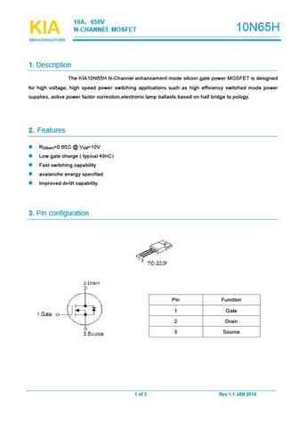
10A 650V 10N65H N-CHANNELMOSFET KIA KIA KIA SEMICONDUCTORS SEMICONDUCTORS SEMICONDUCTORS 1.Description The KIA10N65HN-Channel enhancement mode silicon gate power MOSFETis designed for high voltage, high speed power switching applications such as high efficiency switched mode power supplies, active power factor correction,electronic lampballasts based on half bridge to pology. 2.
sld10n65u.pdf
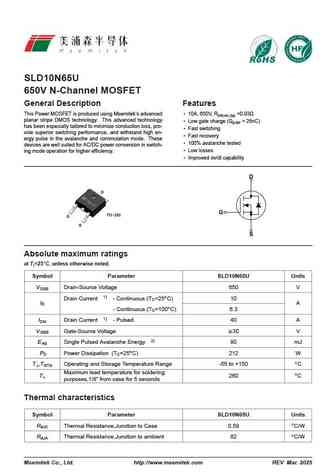
SLD10N65U 650V N-Channel MOSFET General Description Features This Power MOSFET is produced using Msemitek s advanced 10A, 650V, RDS(on),typ =0.93 planar stripe DMOS technology. This advanced technology Low gate charge (Qg,typ = 26nC) has been especially tailored to minimize conduction loss, pro- Fast switching vide superior switching performance, and withstand high en-
slp10n65c slf10n65c.pdf
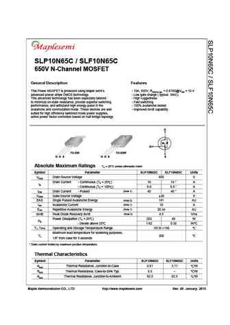
SLP10N65C / SLF10N65C 650V N-Channel MOSFET General Description Features This Power MOSFET is produced using Maple semi s - 10A, 650V, RDS(on) typ. = 0.678 @VGS = 10 V advanced planar stripe DMOS technology. - Low gate charge ( typical 38nC) This advanced technology has been especially tailored - High ruggedness to minimize on-state resistance, provide superior switching - Fast switchi
slp10n65s slf10n65s.pdf

LEAD FREE Pb RoHS SLP10N65S/ SLF10N65S 650V N-Channel MOSFET General Description Features This Power MOSFET is produced using Maple semi s - 10A, 650V, RDS(on) typ=0.8 @VGS = 10 V advanced planar stripe DMOS technology. - Low gate charge ( typical 28.5nC) This advanced technology has been especially tailored - High ruggedness to minimize on-state resistance, provide superior switchi
slf10n65sv.pdf
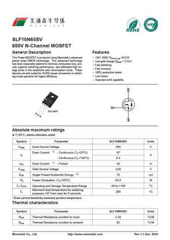
SLF10N65SV 650V N-Channel MOSFET General Description Features This Power MOSFET is produced using Msemitek s advanced 10A*, 650V, RDS(on),typ =0.81 planar stripe DMOS technology. This advanced technology Low gate charge (Qg,typ = 27nC) has been especially tailored to minimize conduction loss, pro- Fast switching vide superior switching performance, and withstand high en-
slp10n65a slf10n65a.pdf
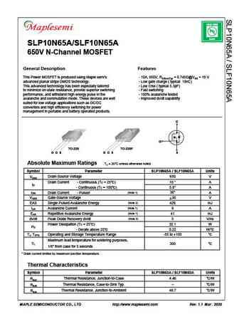
LEAD FREE Pb RoHS SLP10N65A/SLF10N65A 650V N-Channel MOSFET General Description Features This Power MOSFET is produced using Maple semi s - 10A, 650V, RDS(on)Typ = 0.745 @VGS = 10 V advanced planar stripe DMOS technology. - Low gate charge ( typical 19nC) This advanced technology has been especially tailored - Low Crss ( typical 5.3pF) to minimize on-state resistance, provide superi
psa10n65c.pdf
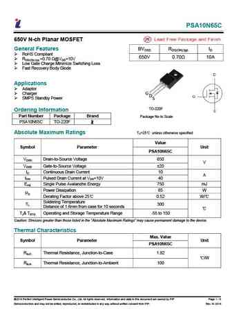
PSA10N65C 650V N-ch Planar MOSFET General Features BVDSS RDS(ON),typ. ID RoHS Compliant 650V 0.70 10A RDS(ON),typ.=0.70 @VGS=10V Low Gate Charge Minimize Switching Loss Fast Recovery Body Diode Applications Adaptor Charger G D SMPS Standby Power S TO-220F Ordering Information Part Number Package Brand Package No to Scale PSA1
swf10n65d swmn10n65d swy10n65d swp10n65d swu10n65d swj10n65d.pdf
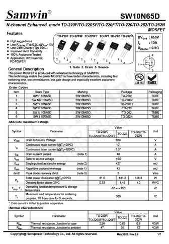
SW10N65D N-channel Enhanced mode TO-220F/TO-220SF/TO-220FT/TO-220/TO-262/TO-262N MOSFET Features TO-262 TO-262N TO-220F TO-220SF TO-220FT TO-220 BVDSS 650V High ruggedness ID 10A Low RDS(ON) (Typ 0.9 )@VGS=10V Low Gate Charge (Typ 35nC) RDS(ON) 0.9 Improved dv/dt Capability 100% Avalanche Tested 2 Application UPS,Inverter, 1 1 1 2 2 1 1 1
swp10n65k swf10n65k swn10n65k swd10n65k swu10n65k swmn10n65k.pdf
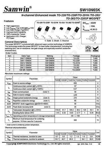
SW10N65K N-channel Enhanced mode TO-220/TO-220F/TO-251N /TO-252/ TO-262/TO-220SF MOSFET Features TO-220F TO-251N TO-262 TO-220 TO-252 TO-220SF BVDSS 650V High ruggedness ID 10A Low RDS(ON) (Typ 0.36 )@VGS=10V RDS(ON) 0.36 Low Gate Charge (Typ29nC) Improved dv/dt Capability 100% Avalanche Tested 2 1 2 1 2 1 2 1 2 1 2 1 2 Applicatio
sw10n65 swp10n65 swf10n65.pdf
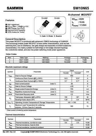
SAMWIN SW10N65 N-channel MOSFET TO-220F TO-220 BVDSS 650V Features ID 10.0A High ruggedness RDS(ON) 1.1ohm RDS(ON) (Max 1.1 )@VGS=10V Gate Charge (Typ 47nC) Improved dv/dt Capability 1 1 2 2 2 100% Avalanche Tested 3 3 1. Gate 2. Drain 3. Source 1 General Description 3 This power MOSFET is produced with advanced VDMOS technology of SAMWIN. This
swf10n65k2 swd10n65k2 swb10n65k2.pdf
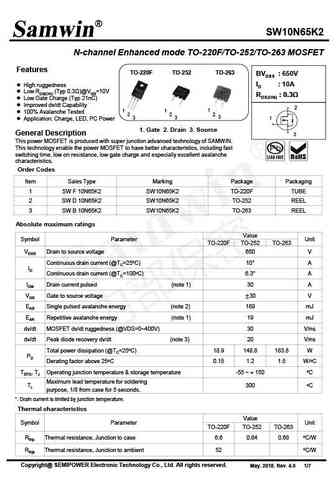
SW10N65K2 N-channel Enhanced mode TO-220F/TO-252/TO-263 MOSFET Features TO-220F TO-252 TO-263 BVDSS 650V High ruggedness ID 10A Low RDS(ON) (Typ 0.3 )@VGS=10V RDS(ON) 0.3 Low Gate Charge (Typ 21nC) Improved dv/dt Capability 2 1 1 1 100% Avalanche Tested 2 2 2 3 3 3 1 Application Charge, LED, PC Power 1. Gate 2. Drain 3. Sou
srm10n65.pdf
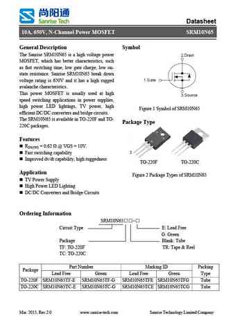
Datasheet 10A, 650V, N-Channel Power MOSFET SRM10N65 General Description Symbol The Sanrise SRM10N65 is a high voltage power MOSFET, which has better characteristics, such as fast switching time, low gate charge, low on- state resistance. Sanrise SRM10N65 break down voltage rating is 650V and it has a high rugged avalanche characteristics. This power MOSFET is usually used at hi
hfs10n65s.pdf
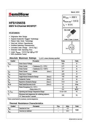
March 2014 BVDSS = 650 V RDS(on) typ HFS10N65S ID = 9.5 A 650V N-Channel MOSFET TO-220F FEATURES 1 Originative New Design 2 3 Superior Avalanche Rugged Technology 1.Gate 2. Drain 3. Source Robust Gate Oxide Technology Very Low Intrinsic Capacitances Excellent Switching Characteristics Unrivalled Gate Charge 29 nC (Typ.) Extended Safe Operating Area
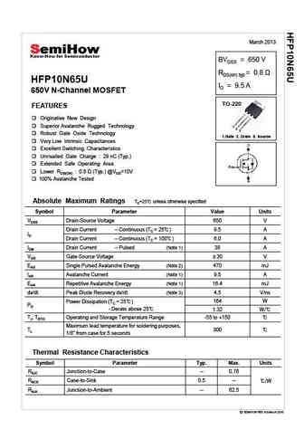
hfs10n65u.pdf
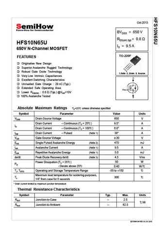
Oct 2013 BVDSS = 650 V RDS(on) typ = 0.8 HFS10N65U ID = 9.5 A 650V N-Channel MOSFET TO-220F FEATURES Originative New Design Superior Avalanche Rugged Technology 1 2 3 Robust Gate Oxide Technology 1.Gate 2. Drain 3. Source Very Low Intrinsic Capacitances Excellent Switching Characteristics Unrivalled Gate Charge 29 nC (Typ.) Extended Safe Operating Area Lo
hfp10n65s.pdf
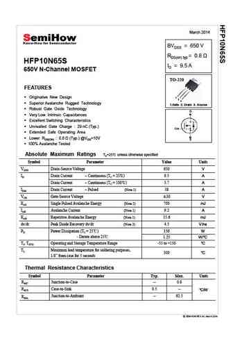
March 2014 BVDSS = 650 V RDS(on) typ HFP10N65S ID = 9.5 A 650V N-Channel MOSFET TO-220 FEATURES Originative New Design 1 2 3 Superior Avalanche Rugged Technology 1.Gate 2. Drain 3. Source Robust Gate Oxide Technology Very Low Intrinsic Capacitances Excellent Switching Characteristics Unrivalled Gate Charge 29 nC (Typ.) Extended Safe Operating Area L
hfp10n65u.pdf
March 2013 BVDSS = 650 V RDS(on) typ = 0.8 HFP10N65U ID = 9.5 A 650V N-Channel MOSFET TO-220 FEATURES Originative New Design Superior Avalanche Rugged Technology 1 2 3 Robust Gate Oxide Technology 1.Gate 2. Drain 3. Source Very Low Intrinsic Capacitances Excellent Switching Characteristics Unrivalled Gate Charge 29 nC (Typ.) Extended Safe Operating Area L
hfs10n65js.pdf
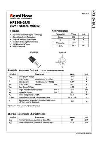
Feb 2023 HFS10N65JS 650V N-Channel MOSFET Features Key Parameters Parameter Value Unit Superior Avalanche Rugged Technology BVDSS 650 V Robust Gate Oxide Technology Very Low Intrinsic Capacitances ID 10 A Excellent Switching Characteristics RDS(on), Typ 0.82 100% Avalanche Tested Qg, Typ 36.3 nC RoHS Compliant TO-220FS Symbol S D G Absolute Maximum
sl10n65f.pdf
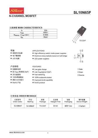
SL10N65F N-CHANNEL MOSFET MAIN CHARACTERISTICS 10A I D 650V V DSS 0.94 R V =10V DS(ON) GS 35nC Q G APPLICATIONS High efficiency switch mode power supplies Electronic lamp ballasts based on half bridge LED LED power supplies FEATURES 1 Gate
tmp10n65 tmpf10n65.pdf
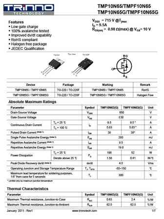
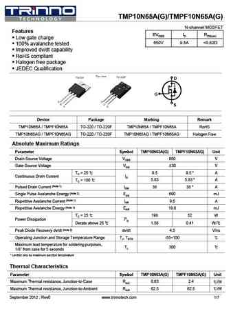
TMP10N65/TMPF10N65 TMP10N65G/TMPF10N65G VDSS = 715 V @Tjmax Features ID = 9.5A Low gate charge RDS(on) = 0.98 W(max) @ VGS= 10 V 100% avalanche tested Improved dv/dt capability RoHS compliant Halogen free package JEDEC Qualification D G S Device Package Marking Remark TMP10N65 / TMPF10N65 TO-220 / TO-220F TMP10N65 / TMPF10N65 RoHS TMP10N
tmp10n65a tmpf10n65a.pdf
TMP10N65A(G)/TMPF10N65A(G) N-channel MOSFET Features BVDSS ID RDS(on) Low gate charge 650V 9.5A
tsp10n65m tsf10n65m.pdf
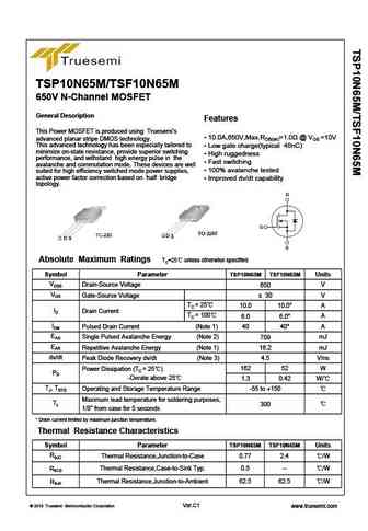
TSP10N65M/TSF10N65M 650V N-Channel MOSFET General Description Features This Power MOSFET is produced using Truesemi s 10.0A,650V,Max.RDS(on)=1.0 @ VGS =10V advanced planar stripe DMOS technology. This advanced technology has been especially tailored to Low gate charge(typical 48nC) minimize on-state resistance, provide superior switching High ruggedness performance, a
wml10n65d1b wmk10n65d1b.pdf
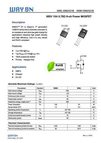
WML10N65D1B WMK10N65D1B 650V 10A 0.75 N-ch Power MOSFET Description TO-220 TO-220F WMOSTM D1 is Wayon s 1st generation TAB VDMOS family that is dramatic reduction in on-resistance and ultra-low gate charge for applications requiring high power density and high efficiency. And it is very robust and RoHS compliant. G G D S D S Features V =700V@T DS jmax
wmm10n65c4 wml10n65c4 wmo10n65c4 wmn10n65c4 wmp10n65c4 wmk10n65c4.pdf

WMM10N65C4, WML10N6 WM C4 65C4, MO10N65C WMN10N65C4, WMP10N6 WM C4 65C4, MK10N65C 650V 0.52 S T V Super Junction Power MOSFET Descrip ption WMOSTM C4 is Wa 4th generation super ayon s n junction MOSFET fa that is utilizing charge M amily S balance te or extremely esistance echnology fo y low on-re D S D G G G S D G and low ga charge performanc WMOSTM
wml10n65em wmk10n65em wmm10n65em wmn10n65em wmp10n65em wmo10n65em.pdf
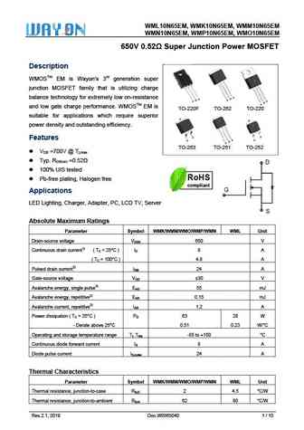
WML10 WMK10N6 0N65EM, W 65EM, WMM10N65EM WMN10 WMP10N6 0N65EM, W 65EM, WMO10N65EM 650V 0.52 S T V Super Junction Power MOSFET Descrip ption WMOSTM EM is Wayon s 3rd generation super W n junction MOSFET fa that is utilizing charge M amily S balance te or extremely esistance echnology fo y low on-re S D D G G G S D G T and low ga ce. WMOSTM EM is ate
cs10n65fa9hd.pdf
Silicon N-Channel Power MOSFET R CS10N65F A9HD VDSS 650 V General Description ID 10 A CS10N65F A9HD, the silicon N-channel Enhanced PD (TC=25 ) 50 W VDMOSFETs, is obtained by the self-aligned planar RDS(ON)Typ 0.65 Technology which reduce the conduction loss, improve switching performance and enhance the avalanche energy. The transistor can be used in vario
gn10n65a4.pdf
Silicon N-Channel Power MOSFET R GN10N65 A4 General Description VDSS 650 V GN10N65 A4, the silicon N-channel Enhanced ID 10 A PD(TC=25 ) 110 W VDMOSFETs, is obtained by the double-shield Technology RDS(ON)Typ 0.9 which reduce the conduction loss, improve switching performance and enhance the avalanche energy. The transistor can be used in various power swi
cs10n65a8hd.pdf
Silicon N-Channel Power MOSFET R CS10N65 A8HD VDSS 650 V General Description ID 10 A CS10N65 A8HD, the silicon N-channel Enhanced PD (TC=25 ) 130 W VDMOSFETs, is obtained by the self-aligned planar RDS(ON)Typ 0.65 Technology which reduce the conduction loss, improve switching performance and enhance the avalanche energy. The transistor can be used in various
cs10n65fa9r.pdf
Silicon N-Channel Power MOSFET R CS10N65F A9R General Description VDSS 650 V CS10N65F A9R, the silicon N-channel Enhanced ID 10 A PD(TC=25 ) 40 W VDMOSFETs, is obtained by the self-aligned planar Technology RDS(ON)Typ 0.86 which reduce the conduction loss, improve switching performance and enhance the avalanche energy. The transistor can be used in various p
atm10n65tf.pdf
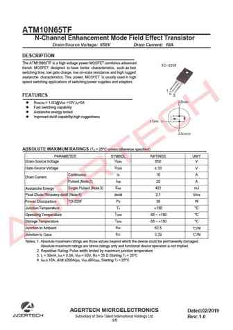
ATM10N65TF N-Channel Enhancement Mode Field Effect Transistor Drain-Source Voltage 650V Drain Current 10A DESCRIPTION The ATM10N65TF is a high voltage power MOSFET combines advanced trench MOSFET designed to have better characteristics, such as fast switching time, low gate charge, low on-state resistance and high rugged avalanche characteristics. This power MOSFET is usually used in h
au10n65s.pdf
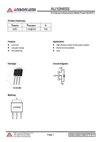
AU10N65S N-Channel Enhancement Mode Power MOSFET Product Summary V(BR)DSS RDS(on)MAX ID 650V 1.3 @10V 10A Feature Application Low Crss High efficiency switch mode power supplies Low gate charge Electronic lamp ballasts Fast switching UPS Package Circuit diagram TO-251AB Marking D U10N65S G D S Document ID Issued Date Revised Date Revision Page. Page 1 AS-3
cs10n65ff.pdf
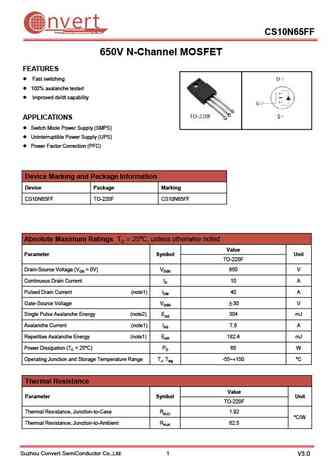
nvert Suzhou Convert Semiconductor Co ., Ltd. CS10N65FF 650V N-Channel MOSFET FEATURES Fast switching 100% avalanche tested Improved dv/dt capability APPLICATIONS Switch Mode Power Supply (SMPS) Uninterruptible Power Supply (UPS) Power Factor Correction (PFC) Device Marking and Package Information Device Package Marking CS10N65FF TO-220F CS10N65FF Absolute
cs10n65f cs10n65p cs10n65k.pdf
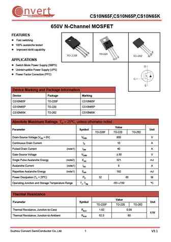
nvert Suzhou Convert Semiconductor Co ., Ltd. CS10N65F,CS10N65P,CS10N65K 650V N-Channel MOSFET FEATURES Fast switching 100% avalanche tested Improved dv/dt capability APPLICATIONS Switch Mode Power Supply (SMPS) Uninterruptible Power Supply (UPS) Power Factor Correction (PFC) Device Marking and Package Information Device Package Marking CS10N65F TO-220F CS1
fir10n65fg.pdf
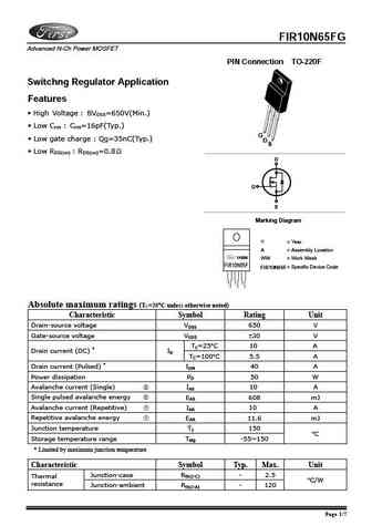
FIR10N65FG Advanced N-Ch Power MOSFET PIN Connection TO-220F Switchng Regulator Application Features High Voltage BVDSS=650V(Min.) Low Crss Crss=16pF(Typ.) G Low gate charge Qg=35nC(Typ.) D S Low RDS(on) RDS(on)=0.8 D G S Marking Diagram Y = Year A = Assembly Location YAWW WW = Work Week FIR10N65F FIR10N65F = Specific Device Code Absolu
smf10n65.pdf
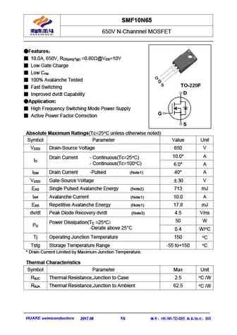
SMF10N65 650V N-Channnel MOSFET Features 10.0A, 650V, R =0.80 @V =10V DS(on)(Typ) GS Low Gate Charge Low C rss 100% Avalanche Tested Fast Switching Improved dv/dt Capability Application High Frequency Switching Mode Power Supply Active Power Factor Correction Absolute Maximum Ratings(Tc=25 C unless otherwise noted) Symbol Parameter Va
hsf10n65.pdf
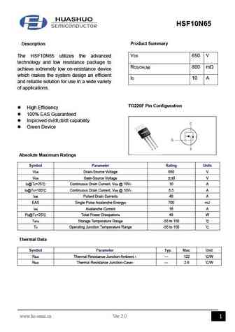
HSF10N65 Product Summary Description VDS 650 V The HSF10N65 utilizes the advanced technology and low resistance package to RDS(ON),typ 800 m achieve extremely low on-resistance device which makes the system design an efficient ID 10 A and reliable solution for use in a wide variety of applications. TO220F Pin Configuration High Efficiency 100% EAS Guarante
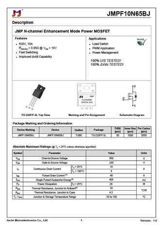
jmpf10n65bj.pdf
JMPF10N65BJ Description JMP N-channel Enhancement Mode Power MOSFET Features Applications 650V, 10A Load Switch RDS(ON)
jjt10n65sc.pdf
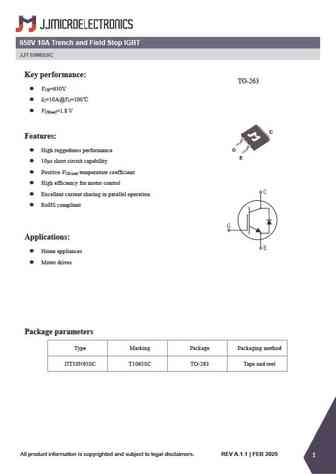
650V 10A Trench and Field Stop IGBT JJT10N65SC Key performance TO-263 V =650V CE I =10A@T =100 C C V =1.8 V CE(sat) C Features G High ruggedness performance E 10 s short circuit capability Positive V temperature coefficient CE (sat) High efficiency for motor control Excellent current sharing in parallel operation RoHS compliant Appl
jjt10n65st.pdf
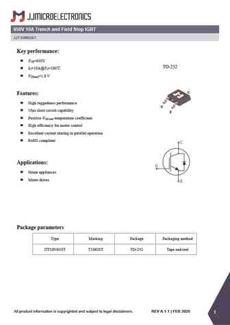
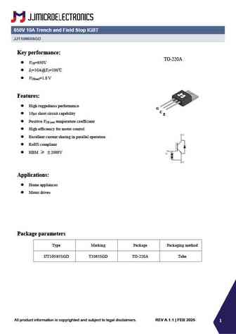
650V 10A Trench and Field Stop IGBT JJT10N65ST Key performance V =650V CE TO-252 I =10A@T =100 C C V =1.8 V CE(sat) C Features High ruggedness performance G 10 s short circuit capability E Positive V temperature coefficient CE (sat) High efficiency for motor control Excellent current sharing in parallel operation RoHS compliant Appl
jjt10n65scd.pdf
650V 10A Trench and Field Stop IGBT JJT10N65SCD Key performance TO-263 V =650V CE I =10A@T =100 C C V =1.8 V CE(sat) C Features G High ruggedness performance E 10 s short circuit capability Positive V temperature coefficient CE (sat) High efficiency for motor control Excellent current sharing in parallel operation RoHS compliant
jjt10n65ss.pdf
650V 10A Trench and Field Stop IGBT JJT10N65SS Key performance V =650V CE TO-220F I =10A@T =100 C C V =1.8 V CE(sat) Features High ruggedness performance 10 s short circuit capability G C E Positive V temperature coefficient CE (sat) High efficiency for motor control Excellent current sharing in parallel operation RoHS compliant App
jmpc10n65bj.pdf
JMPC10N65BJ Description JMP N-channel Enhancement Mode Power MOSFET Features Applications 650V, 10A Load Switch RDS(ON)
lnd10n65 lnc10n65 lne10n65 lnf10n65 lndn10n65.pdf
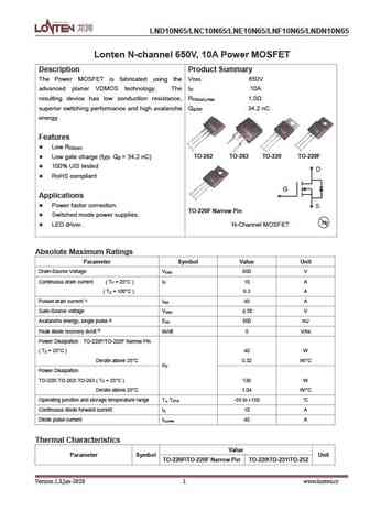
LND10N65/LNC10N65/LNE10N65/LNF10N65/LNDN10N65 Lonten N-channel 650V, 10A Power MOSFET Description Product Summary The Power MOSFET is fabricated using the V 650V DSS advanced planer VDMOS technology. The I 10A D resulting device has low conduction resistance, R 1.0 DS(on),max superior switching performance and high avalanche Q 34.2 nC g,typ energy. Features Low R DS(on)
lnd10n65 lnc10n65 lne10n65 lnf10n65.pdf
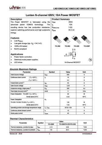
LND10N65/LNC10N65/LNE10N65/LNF10N65 Lonten N-channel 650V, 10A Power MOSFET Description Product Summary The Power MOSFET is fabricated using the VDSS 650V advanced planer VDMOS technology. The ID 10A resulting device has low conduction resistance, RDS(on),max 1.0 superior switching performance and high avalanche Qg,typ 34.2 nC energy. Features Low RDS(on) Low gate
f10n65.pdf
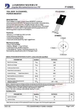
Jingdao Microelectronics co.LTD F10N65 ITO-220ABW 10A, 650V N-CHANNEL POWER MOSFET DESCRIPTION The F10N65 is a high voltage power MOSFET combines advanced trench MOSFET designed to have better characteristics, such as fast switching time, low gate charge, low on-state resistance and high rugged avalanche characteristics. This pow
ptf10n65.pdf
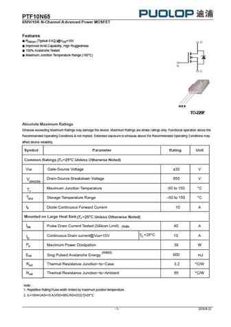
PTF1 0N65 65 0V/1 0A N-Channel A dv anced Power MOSFET Features RDS(on) (Typical 0.6 )@VGS=10V Improved dv/dt Capability, High Ruggedness 100% Avalanche Tested Maximum Junction Temperature Range (150 C) G D S TO-220F Absolute Maximum Ratings Stresses exceeding Maximum Ratings may damage the device. Maximum Ratings are stress ratings only. Functional operation above
agm10n65f.pdf
AGM10N65F Table 3. Electrical Characteristics (TJ=25 unless otherwise noted) Symbol Parameter Conditions Min Typ Max Unit On/Off States BVDSS Drain-Source Breakdown Voltage V =0V I =250 A GS D 650 -- -- V Zero Gate Voltage Drain Current V =650V,V =0V -- -- 1 A DS GS I DSS Gate-Body Leakage Current V = 30V,V =0V -- -- nA GS DS I GSS 100 VGS(th) Gate Threshold Voltage
spc10n65g.pdf
SPC10N65G Sinai Power Technologies www.sinai-power.com N-channel Power MOSFET PRODUCT SUMMARY Features V (V) at T max. 700 DS J ID=10A(Vgs=10V) R max. at 25oC ( ) V =10V 1.1 DS(on) GS Ultra Low Gate Charge Q max. (nC) 45 g Improved dv/dt Capability Q (nC) 7 gs 100% Avalanche Tested Q (nC) 15 gd RoHS compliant Configuration single App
wsr10n65f.pdf
WSR10N65F N-Ch MOSFET General Description Product Summery The WSR10N65F is the highest performance trench RDSON ID BVDSS N-Ch MOSFET with extreme high cell density,which provide excellent RDSON and gate charge for most 650V 0.8 10A of the synchronous buck converter applications . Applications The WSR10N65F meet the RoHS and Green Product requirement , 100% EAS AC/DC
smirf10n65.pdf
SMIRF10N65 30V /36A Single N Power MOSFET N-Channel Enhancement Mode Power MOSFET Description ID 10A SMIRF10N65 is an N-channel enhancement mode power MOS field effect transistor. The improved VDSS 650V planar stripe cell and the improved guard ring terminal have been especially tailored to minimize Rdson max 1.0 (VGS=10V, ID=5A) on-state resistance, provide superior
vbzmb10n65.pdf
VBZMB10N65 www.VBsemi.com N hannel 650 D S Power MOSFET FEATURES PRODUCT SUMMARY VDS (V) at TJ max. 650 Low figure-of-merit (FOM) Ron x Qg Low input capacitance (Ciss) RDS(on) max. at 25 C ( ) VGS = 10 V 0.9 Reduced switching and conduction losses Qg max. (nC) 57 Ultra low gate charge (Qg) Qgs (nC) 4.0 Avalanche energy rated (UIS) Qgd (nC) 5.4 Config
dgp10n65ctl.pdf
RoHS DGP10N65CTL COMPLIANT IGBT Descrete V 650 V CE I 10 A C V I = A 1.65 V CE(SAT) C 10 Applications Soft switchingapplications Circuit Airconditioning Motor driveinverter Features High speed smooth switching device for hard & soft switching Maximum junction temperature 175 Positive temperature coefficient High ruggedness,
tma10n65h tmp10n65h.pdf
TMA10N65H, TMP10N65H Wuxi Unigroup Microelectronics Company 650V N-Channel MOSFET FEATURES Fast switching 100% avalanche tested Improved dv/dt capability APPLICATIONS Switch Mode Power Supply (SMPS) Uninterruptible Power Supply (UPS) Power Factor Correction (PFC) Device Marking and Package Information Device Package Marking TMA10N65H TO-220F A1
mpf10n65.pdf
Silicon N-Channel Power MOSFET Description The MPF10N65 uses advanced trench technology and design to provide excellent RDS(ON)with low gate charge. It can be used in a wide variety of applications. General Features VDS=10A ID=650V Schematic diagram RDS(on)(typ)=0.6 @VGS=10V,ID=4.0A Low Crss 18.5pF@25V Fast switching Improved dv/dt capability Application
fxn10n65f.pdf
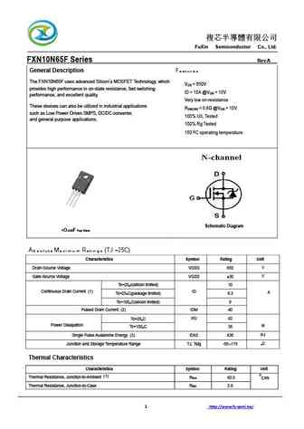
FuXin Semiconductor Co., Ltd. FXN10N65F Series Rev.A General Description Features The FXN10N65F uses advanced Silicon s MOSFET Technology, which V = 650V DS provides high performance in on-state resistance, fast switching ID = 10A @V = 10V GS performance, and excellent quality. Very low on-resistance These devices can also be utilized in in
mpva10n65f.pdf
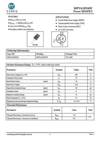
MPVA10N65F Power MOSFET MPSW60M041 FEATURES APPLICATIONS l BVDSS 650V, ID=10A l Switch Mode Power Supply (SMPS) l RDS(on) 1.1 (Max) @VGS=10V l Uninterruptible Power Supply (UPS) l Very Low FOM (RDS(on) *Qg) l Power Factor Correction (PFC) l Excellent stability and uniformity l AC to DC Converters D G TO-220F S Ordering Information Type NO. Marking Package Code MPVA10N6
mpbp10n65ef mpba10n65ef mpbd10n65ef.pdf
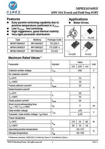
MPBX10N65EF 650V-10A Trench and Field Stop IGBT Features Applications Easy parallel switching capability due to Motor Drives positive temperature coefficient in VCEsat Low VCEsat fast switching High ruggedness, good thermal stability Very tight parameter distribution G C E TO-220 Type Marking Package Code MPBP10N65EF MP10N65EF TO-220-3 MPBA10N65EF MP10N65EF
h10n65p h10n65f.pdf
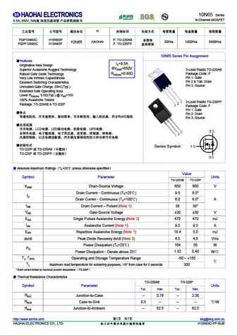
10N65 Series N-Channel MOSFET 9.5A, 650V, N H FQP10N65C H10N65P P TO-220AB HAOHAI 50Pcs 1000Pcs 5000Pcs 10N65 FQPF10N65C H10N65F F TO-220FP 10N65 Series Pin Assignment Features ID=9.5A Originativ
fcb110n65f.pdf
isc N-Channel MOSFET Transistor FCB110N65F FEATURES Drain Current I = 35A@ T =25 D C Drain Source Voltage- V = 650V(Min) DSS Static Drain-Source On-Resistance R = 110m (Max) DS(on) 100% avalanche tested Minimum Lot-to-Lot variations for robust device performance and reliable operation DESCRIPTION Designed for use in switch mode power supplies and general pu
aot10n65.pdf
isc N-Channel MOSFET Transistor AOT10N65 FEATURES Drain Current I = 10A@ T =25 D C Drain Source Voltage- V = 650V(Min) DSS Static Drain-Source On-Resistance R = 1.0 (Max) DS(on) 100% avalanche tested Minimum Lot-to-Lot variations for robust device performance and reliable operation DESCRIPTION Designed for use in switch mode power supplies and general purpo
aotf10n65.pdf
isc N-Channel MOSFET Transistor AOTF10N65 FEATURES With TO-220F packaging High speed switching Low gate input resistance Standard level gate drive Easy to use 100% avalanche tested Minimum Lot-to-Lot variations for robust device performance and reliable operation APPLICATIONS Power supply Switching applications ABSOLUTE MAXIMUM RATINGS(T =25 ) a SYMBOL P
aow10n65.pdf
isc N-Channel MOSFET Transistor AOW10N65 FEATURES Drain Current I = 10A@ T =25 D C Drain Source Voltage- V = 650V(Min) DSS Static Drain-Source On-Resistance R = 1.0 (Max) DS(on) 100% avalanche tested Minimum Lot-to-Lot variations for robust device performance and reliable operation DESCRIPTION Designed for use in switch mode power supplies and general purpo
ap10n65f ap10n65p.pdf
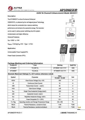
AP10N65FIP 650V N-Channel Enhancement Mode MOSFET Description The AP10N65F/P is silicon N-channel Enhanced VDMOSFETs, is obtained by the self-aligned planar Technology which reduce the conduction loss, improve switching performance and enhance the avalanche energy. The transistor can be used in various power switching circuit for system miniaturization and higher efficiency.
apj10n65d ap65r950.pdf
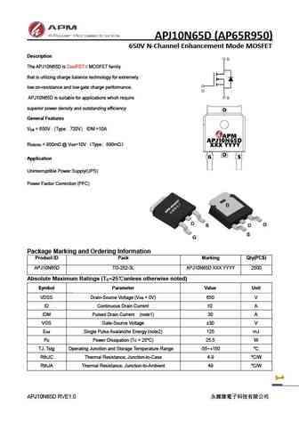
APJ10N65D (AP65R950) 650V N-Channel Enhancement Mode MOSFET Description The APJ10N65D is CoolFET II MOSFET family that is utilizing charge balance technology for extremely low on-resistance and low gate charge performance. APJ10N65D is suitable for applications which require superior power density and outstanding efficiency General Features V = 650V Type 720V IDM =10A
apj10n65f apj10n65t apj10n65p ap65r950.pdf
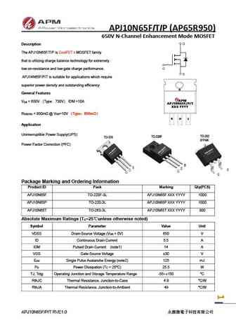
APJ10N65FITIP (AP65R950) 650V N-Channel Enhancement Mode MOSFET Description The APJ10N65F/T/P is CoolFET II MOSFET family that is utilizing charge balance technology for extremely low on-resistance and low gate charge performance. APJ14N65F/P/T is suitable for applications which require superior power density and outstanding efficiency General Features V = 650V Type 730V
Otros transistores... 15N70, 6N65Z, 7N65A, 7N65, 7N65Z, 7N65K, 8N65, 9N65, 10N65, 10N65Z, 10N65K, 15N65, 18N65, 20N65, 22N65, 1N65A, 1N65
Parámetros del MOSFET. Cómo se afectan entre sí.
History: CEH2313
🌐 : EN ES РУ

Liste
Recientemente añadidas las descripciónes de los transistores:
MOSFET: BC2301 | BC1012W | BC1012T | BC1012 | 2SK3019WT | 2SK3019W | 2SK3018WT | CS95118 | CS85105A | CS75N45 | CS72N12 | CS55N50 | CS48N75A | CS40N27 | MSQ60P04D | MSQ40P07D
Popular searches
tl431 datasheet | 2sd526 | 2n4403 transistor equivalent | 2sc1318 | 2n3055 transistor equivalent | 2sc1740 | c3229 | c2078 transistor