3N60 Datasheet. Equivalente. Reemplazo. Hoja de especificaciones. Principales características
Número de Parte: 3N60 📄📄
Tipo de FET: MOSFET
Polaridad de transistor: N
ESPECIFICACIONES MÁXIMAS
Pdⓘ - Máxima disipación de potencia: 75 W
|Vds|ⓘ - Voltaje máximo drenador-fuente: 600 V
|Vgs|ⓘ - Voltaje máximo fuente-puerta: 30 V
|Id|ⓘ - Corriente continua de drenaje: 3 A
Tjⓘ - Temperatura máxima de unión: 150 °C
CARACTERÍSTICAS ELÉCTRICAS
trⓘ - Tiempo de subida: 30 nS
Cossⓘ - Capacitancia de salida: 50 pF
RDSonⓘ - Resistencia estado encendido drenaje a fuente: 2.8 Ohm
📄📄 Copiar
Búsqueda de reemplazo de 3N60 MOSFET
- Selecciónⓘ de transistores por parámetros
3N60 datasheet
3n60.pdf
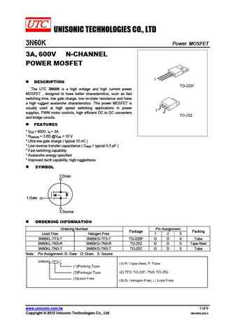
UNISONIC TECHNOLOGIES CO., LTD 3N60 Power MOSFET 3A, 600V N-CHANNEL POWER MOSFET DESCRIPTION The UTC 3N60 is a high voltage and high current power MOSFET , designed to have better characteristics, such as fast switching time, low gate charge, low on-state resistance and have a high rugged avalanche characteristics. This power MOSFET is usually used at high speed switching ap
3n60.pdf
isc N-Channel MOSFET Transistor 3N60 FEATURES Drain Current I =3.0A@ T =25 D C Drain Source Voltage- V = 600V(Min) DSS Static Drain-Source On-Resistance R = 2.5 (Max) DS(on) Fast Switching Minimum Lot-to-Lot variations for robust device performance and reliable operation APPLICATIONS Switching power supplies,converters,AC and DC motor controls ABSOLUTE M
hgtd3n60c3s hgtp3n60c3.pdf
HGTD3N60C3S, HGTP3N60C3 Data Sheet December 2001 6A, 600V, UFS Series N-Channel IGBTs Features The HGTD3N60C3S and the HGTP3N60C3 are MOS gated 6A, 600V at TC = 25oC high voltage switching devices combining the best features 600V Switching SOA Capability of MOSFETs and bipolar transistors. These devices have Typical Fall Time. . . . . . . . . . . . . . . . 130ns at TJ = 1
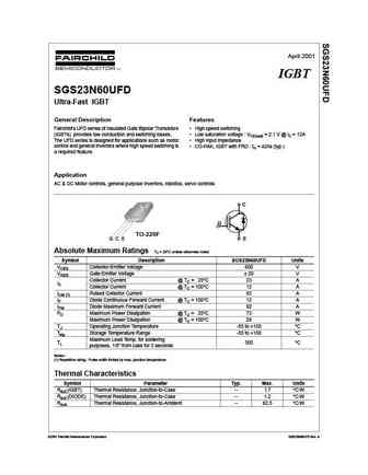
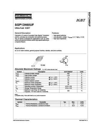
sgs23n60uf.pdf
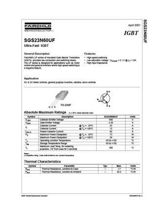
April 2001 IGBT SGS23N60UF Ultra-Fast IGBT General Description Features Fairchild's UF series of Insulated Gate Bipolar Transistors High speed switching (IGBTs) provides low conduction and switching losses. Low saturation voltage VCE(sat) = 2.1 V @ IC = 12A The UF series is designed for applications such as motor High input impedance control and general inverters where h
dmg3n60sct.pdf
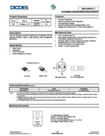
DMG3N60SCT N-CHANNEL ENHANCEMENT MODE MOSFET Product Summary Features Low Input Capacitance ID BVDSS RDS(ON) Package High BVDSS Rating for Power Application TC = +25 C TO220AB Low Input/Output Leakage 600V 3.5 @VGS = 10V 3.3A (Type TH) Lead-Free Finish; RoHS Compliant (Notes 1 & 2) Halogen and Antimony Free. Green Device (Note 3) Mechanica
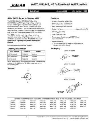
hgtp3n60b3d hgt1s3n60b3ds.pdf
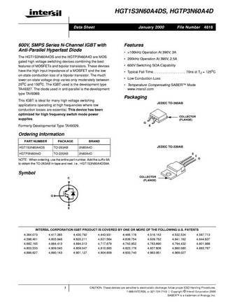
HGTP3N60B3D, HGT1S3N60B3DS Data Sheet January 2000 File Number 4414.1 7A, 600V, UFS Series N-Channel IGBT with Features Anti-Parallel Hyperfast Diode 7A, 600V TC = 25oC The HGTP3N60B3D and HGT1S3N60B3DS are MOS gated 600V Switching SOA Capability high voltage switching devices combining the best features Typical Fall Time. . . . . . . . . . . . . . . . 115ns at TJ = 125oC o
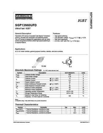
sgs13n60ufd.pdf

April 2001 IGBT SGS13N60UFD Ultra-Fast IGBT General Description Features Fairchild's UFD series of Insulated Gate Bipolar Transistors High speed switching (IGBTs) provides low conduction and switching losses. Low saturation voltage VCE(sat) = 2.1 V @ IC = 6.5A The UFD series is designed for applications such as motor High input impedance control and general inverters whe
sgs13n60uf.pdf

April 2001 IGBT SGS13N60UF Ultra-Fast IGBT General Description Features Fairchild's UF series of Insulated Gate Bipolar Transistors High speed switching (IGBTs) provides low conduction and switching losses. Low saturation voltage VCE(sat) = 2.1 V @ IC = 6.5A The UF series is designed for applications such as motor High input impedance control and general inverters where
pfp13n60 pff13n60.pdf
Feb 2009 PFP13N60/PFF13N60 FEATURES 600V N-Channel MOSFET Originative New Design 100% EAS Test Rugged Gate Oxide Technology Drain BVDSS = 600 V Extremely Low Intrinsic Capacitances Remarkable Switching Characteristics Gate RDS(on) = 0.51 Unequalled Gate Charge 48 nC (Typ.)
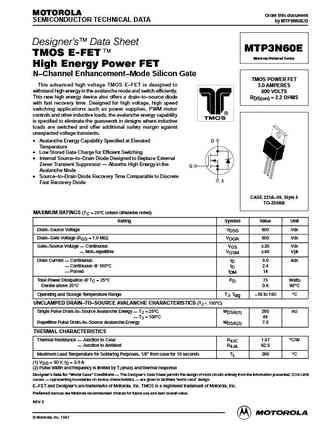
mtp3n60e.pdf

MOTOROLA Order this document SEMICONDUCTOR TECHNICAL DATA by MTP3N60E/D Designer's Data Sheet MTP3N60E TMOS E-FET. Motorola Preferred Device High Energy Power FET N Channel Enhancement Mode Silicon Gate TMOS POWER FET This advanced high voltage TMOS E FET is designed to 3.0 AMPERES withstand high energy in the avalanche mode and switch efficiently. 600 VOLTS This new
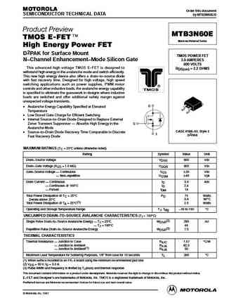
mtb3n60erev0.pdf

MOTOROLA Order this document SEMICONDUCTOR TECHNICAL DATA by MTB3N60E/D Product Preview MTB3N60E TMOS E-FET. Motorola Preferred Device High Energy Power FET D2PAK for Surface Mount TMOS POWER FET 3.0 AMPERES N Channel Enhancement Mode Silicon Gate 600 VOLTS This advanced high voltage TMOS E FET is designed to RDS(on) = 2.2 OHMS withstand high energy in the avalanche mod
mtp3n60erev2.pdf
MOTOROLA Order this document SEMICONDUCTOR TECHNICAL DATA by MTP3N60E/D Designer's Data Sheet MTP3N60E TMOS E-FET. Motorola Preferred Device High Energy Power FET N Channel Enhancement Mode Silicon Gate TMOS POWER FET This advanced high voltage TMOS E FET is designed to 3.0 AMPERES withstand high energy in the avalanche mode and switch efficiently. 600 VOLTS This new
mtb3n60e.pdf
MOTOROLA Order this document SEMICONDUCTOR TECHNICAL DATA by MTB3N60E/D Product Preview MTB3N60E TMOS E-FET. Motorola Preferred Device High Energy Power FET D2PAK for Surface Mount TMOS POWER FET 3.0 AMPERES N Channel Enhancement Mode Silicon Gate 600 VOLTS This advanced high voltage TMOS E FET is designed to RDS(on) = 2.2 OHMS withstand high energy in the avalanche mod
php3n60e phb3n60e.pdf
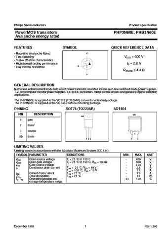
Philips Semiconductors Product specification PowerMOS transistors PHP3N60E, PHB3N60E Avalanche energy rated FEATURES SYMBOL QUICK REFERENCE DATA d Repetitive Avalanche Rated Fast switching VDSS = 600 V Stable off-state characteristics High thermal cycling performance ID = 2.8 A g Low thermal resistance RDS(ON) 4.4 s GENERAL DESCRIPTION N-channel, enh
phx3n60e.pdf
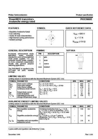
Philips Semiconductors Product specification PowerMOS transistors PHX3N60E Avalanche energy rated FEATURES SYMBOL QUICK REFERENCE DATA d Repetitive Avalanche Rated Fast switching VDSS = 600 V Stable off-state characteristics High thermal cycling performance ID = 1.7 A g Isolated package RDS(ON) 4.4 s GENERAL DESCRIPTION PINNING SOT186A N-channel, enh
stf33n60m2 sti33n60m2 stp33n60m2 stw33n60m2.pdf
STF33N60M2, STI33N60M2, STP33N60M2, STW33N60M2 N-channel 600 V, 0.108 typ., 26 A MDmesh II Plus low Qg Power MOSFETs in TO-220FP, I2PAK, TO-220 and TO-247 packages Datasheet - production data Features TAB VDS @ RDS(on) Order codes ID 3 2 3 TJmax max 1 2 1 2 I PAK TO-220FP STF33N60M2 26 A(1) TAB STI33N60M2 650 V 0.125 STP33N60M2 26 A STW33N60M2 3 3 2 2 1
stl13n60m2.pdf
STL13N60M2 N-channel 600 V, 0.39 typ., 7 A MDmesh II Plus low Qg Power MOSFET in a PowerFLAT 5x6 HV package Datasheet - production data Features Order code VDS @ TJmax RDS(on) max ID STL13N60M2 650 V 0.42 7 A Extremely low gate charge Lower RDS(on) x area vs previous generation 1 2 3 Low gate input resistance 4 100% avalanche tested PowerFLAT 5x6
stb13n60m2 std13n60m2.pdf
STB13N60M2, STD13N60M2 N-channel 600 V, 0.35 typ., 11 A MDmesh II Plus low Qg Power MOSFETs in D2PAK and DPAK packages Datasheet - production data Features Order codes VDS @ TJmax RDS(on) max ID STB13N60M2 TAB 650 V 0.38 11 A STD13N60M2 TAB 3 3 Extremely low gate charge 1 1 Lower RDS(on) x area vs previous generation DPAK D2PAK Low gate input resistance
stp43n60dm2.pdf
STP43N60DM2 N-channel 600 V, 0.085 typ., 34 A MDmesh DM2 Power MOSFET in a TO-220 package Datasheet - production data Features V @ R DS DS(on) Order code I P D TOT TJmax. max. STP43N60DM2 650 V 0.093 34 A 250 W Fast-recovery body diode Extremely low gate charge and input capacitance Low on-resistance 100% avalanche tested Extremely high
stp13n60m2 stu13n60m2 stw13n60m2.pdf
STP13N60M2, STU13N60M2, STW13N60M2 N-channel 600 V, 0.35 typ., 11 A MDmesh II Plus low Qg Power MOSFETs in TO-220, IPAK and TO-247 packages Datasheet - production data Features TAB TAB Order codes VDS @ TJmax RDS(on) max ID 3 2 1 STP13N60M2 3 2 1 IPAK STU13N60M2 650 V 0.38 11 A TO-220 STW13N60M2 Extremely low gate charge Lower RDS(on) x area vs previous g
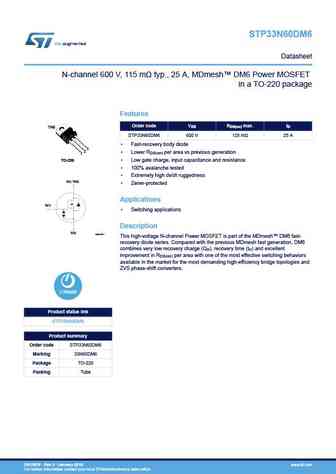
stf33n60dm6.pdf
STF33N60DM6 Datasheet N-channel 600 V, 115 m typ., 25 A, MDmesh DM6 Power MOSFET in a TO 220FP package Features VDS RDS(on) max. ID Order code STF33N60DM6 600 V 128 m 25 A Fast-recovery body diode Lower RDS(on) per area vs previous generation 3 2 1 Low gate charge, input capacitance and resistance 100% avalanche tested TO-220FP Extremely high dv/dt
stf13n60m2 stfi13n60m2.pdf
STF13N60M2, STFI13N60M2 N-channel 600 V, 0.35 typ., 11 A MDmesh II Plus low Qg Power MOSFETs in TO-220FP and I2PAKFP packages Datasheet - production data Features Order codes VDS @ TJmax RDS(on) max ID STF13N60M2 650 V 0.38 11 A STFI13N60M2 3 2 Extremely low gate charge 1 1 2 3 TO-220FP Lower RDS(on) x area vs previous generation I2PAKFP Low gate input r
stb33n60m2.pdf
STB33N60M2 N-channel 600 V, 0.108 typ., 26 A MDmesh II Plus low Qg Power MOSFETs in a D2PAK package Datasheet - production data Features VDS @ RDS(on) TAB Order code ID TJmax max STB33N60M2 650 V 0.125 26 A 3 Extremely low gate charge 1 Lower RDS(on) x area vs previous generation D 2PAK MDmesh II technology Low gate input resistance 100% avalan
stw43n60dm2.pdf
STW43N60DM2 N-channel 600 V, 0.085 typ., 34 A MDmesh DM2 Power MOSFET in a TO-247 package Datasheet - production data Features V @ DS R DS(on) Order code I P D TOT max. TJmax. STW43N60DM2 650 V 0.093 34 A 250 W Fast-recovery body diode 3 Extremely low gate charge and input 2 capacitance 1 Low on-resistance 100% avalanche tested TO-2
stf13n60dm2.pdf

STF13N60DM2 Datasheet N-channel 600 V, 0.310 typ., 11 A MDmesh DM2 Power MOSFET in a TO-220FP package VDS RDS(on) max. ID Order codes STF13N60DM2 600 V 0.365 11 A Fast-recovery body diode Extremely low gate charge and input capacitance Low on-resistance 3 2 1 100% avalanche tested Extremely high dv/dt ruggedness TO-220FP Zener-protected D(2) A
std13n60dm2.pdf
STD13N60DM2 Datasheet N-channel 600 V, 0.310 typ., 11 A MDmesh DM2 Power MOSFET in a DPAK package VDS RDS(on) max. ID Order codes TAB STD13N60DM2 600 V 0.365 11 A Fast-recovery body diode 3 2 1 Extremely low gate charge and input capacitance DPAK Low on-resistance 100% avalanche tested D(2, TAB) Extremely high dv/dt ruggedness Zener-protected
stp13n60dm2.pdf

STP13N60DM2 Datasheet N-channel 600 V, 0.310 typ., 11 A MDmesh DM2 Power MOSFET in a TO-220 package Features VDS RDS(on ) max. ID Order code TAB STP13N60DM2 600 V 0.365 11 A Fast-recovery body diode 3 2 Extremely low gate charge and input capacitance 1 Low on-resistance TO-220 100% avalanche tested Extremely high dv/dt ruggedness D(2, TAB) Ze
mtp3n60.pdf
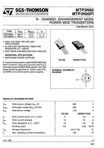
MTP3N60 MTP3N60FI N - CHANNEL ENHANCEMENT MODE POWER MOS TRANSISTOR TYPE V R I DSS DS(on) D MTP3N60 600 V
stp33n60dm6.pdf
STP33N60DM6 Datasheet N-channel 600 V, 115 m typ., 25 A, MDmesh DM6 Power MOSFET in a TO 220 package Features VDS RDS(on) max. ID Order code TAB STP33N60DM6 600 V 128 m 25 A Fast-recovery body diode 3 2 Lower RDS(on) per area vs previous generation 1 TO-220 Low gate charge, input capacitance and resistance 100% avalanche tested Extremely high dv/dt
stl33n60m2.pdf
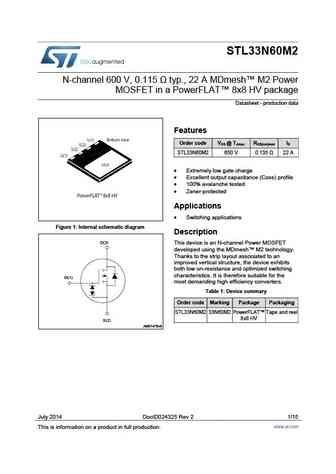
STL33N60M2 N-channel 600 V, 0.115 typ., 22 A MDmesh M2 Power MOSFET in a PowerFLAT 8x8 HV package Datasheet - production data Features Order code V DS @ T R I Jmax DS(on)max D STL33N60M2 650 V 0.135 22 A Extremely low gate charge Excellent output capacitance (Coss) profile 100% avalanche tested Zener-protected Applications Switching app
stb33n60dm2 stp33n60dm2 stw33n60dm2.pdf
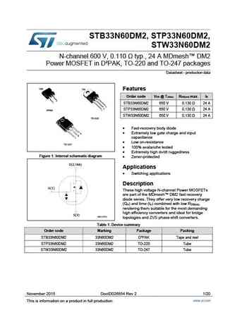
STB33N60DM2, STP33N60DM2, STW33N60DM2 N-channel 600 V, 0.110 typ., 24 A MDmesh DM2 Power MOSFET in D PAK, TO-220 and TO-247 packages Datasheet - production data Features Order code V @ T R max. I DS Jmax. DS(on) D STB33N60DM2 650 V 0.130 24 A STP33N60DM2 650 V 0.130 24 A STW33N60DM2 650 V 0.130 24 A Fast-recovery body diode Extremely low gate charg
stl33n60dm2.pdf
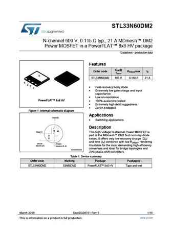
STL33N60DM2 N-channel 600 V, 0.115 typ., 21 A MDmesh DM2 Power MOSFET in a PowerFLAT 8x8 HV package Datasheet - production data Features V DS @ Order code RDS(on)max ID T Jmax 5 STL33N60DM2 650 V 0.140 21 A 4 3 2 Fast-recovery body diode 1 Extremely low gate charge and input capacitance Low on-resistance PowerFLAT 8x8 HV 100% ava
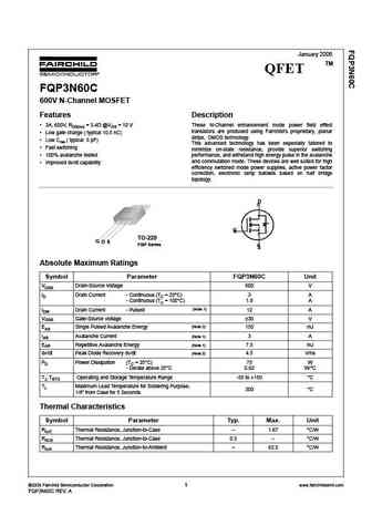
fqu3n60ctu.pdf
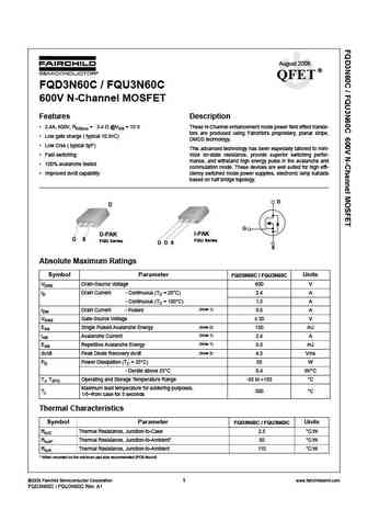
August 2006 QFET FQD3N60C / FQU3N60C 600V N-Channel MOSFET Features Description 2.4A, 600V, RDS(on) = 3.4 @VGS = 10 V These N-Channel enhancement mode power field effect transis- tors are produced using Fairchild s proprietary, planar stripe, Low gate charge ( typical 10.5nC) DMOS technology. Low Crss ( typical 5pF) This advanced technology has been especially t
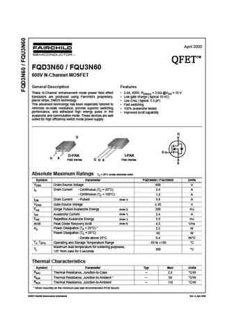
fqd3n60 fqu3n60.pdf

April 2000 TM QFET QFET QFET QFET FQD3N60 / FQU3N60 600V N-Channel MOSFET General Description Features These N-Channel enhancement mode power field effect 2.4A, 600V, RDS(on) = 3.6 @VGS = 10 V transistors are produced using Fairchild s proprietary, Low gate charge ( typical 10 nC) planar stripe, DMOS technology. Low Crss ( typical 5.5 pF) This advanced technology h
sgs23n60ufd.pdf
April 2001 IGBT SGS23N60UFD Ultra-Fast IGBT General Description Features Fairchild's UFD series of Insulated Gate Bipolar Transistors High speed switching (IGBTs) provides low conduction and switching losses. Low saturation voltage VCE(sat) = 2.1 V @ IC = 12A The UFD series is designed for applications such as motor High input impedance control and general inverters wher
fcp13n60n fcpf13n60nt.pdf
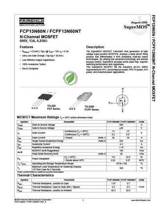
August 2009 SupreMOSTM FCP13N60N / FCPF13N60NT N-Channel MOSFET 600V, 13A, 0.258 Features Description RDS(on) = 0.244 ( Typ.) @ VGS = 10V, ID = 6.5A The SupreMOS MOSFET, Fairchild s next generation of high voltage super-junction MOSFETs, employs a deep trench filling Ultra Low Gate Charge ( Typ.Qg = 30.4nC) process that differentiates it from preceding multi-epi based
sgp23n60ufd.pdf
IGBT SGP23N60UFD Ultra-Fast IGBT General Description Features Fairchild's UFD series of Insulated Gate Bipolar Transistors High speed switching (IGBTs) provides low conduction and switching losses. Low saturation voltage VCE(sat) = 2.1 V @ IC = 12A The UFD series is designed for applications such as motor High input impedance control and general inverters where high speed
fqp3n60.pdf
April 2000 TM QFET QFET QFET QFET FQP3N60 600V N-Channel MOSFET General Description Features These N-Channel enhancement mode power field effect 3.0A, 600V, RDS(on) = 3.6 @VGS = 10 V transistors are produced using Fairchild s proprietary, Low gate charge ( typical 10 nC) planar stripe, DMOS technology. Low Crss ( typical 5.5 pF) This advanced technology has been es
sgp23n60uf.pdf

IGBT SGP23N60UF Ultra-Fast IGBT General Description Features Fairchild's UF series of Insulated Gate Bipolar Transistors High speed switching (IGBTs) provides low conduction and switching losses. Low saturation voltage VCE(sat) = 2.1 V @ IC = 12A The UF series is designed for applications such as motor High input impedance control and general inverters where high speed sw
fqd3n60ctm ws.pdf
November 2013 FQD3N60CTM_WS N-Channel QFET MOSFET 600 V, 2.4 A, 3.4 Features Description 2.4 A, 600 V, RDS(on) = 3.4 (Max.) @ VGS = 10 V, ID = 1.2 A This N-Channel enhancement mode power MOSFET is produced using Fairchild Semiconductor s proprietary Low Gate Charge (Typ. 10.5 nC) planar stripe and DMOS technology. This advanced Low Crss (Typ. 5 pF) MOSFET te
sgh23n60ufd.pdf
September 2000 IGBT SGH23N60UFD Ultra-Fast IGBT General Description Features Fairchild's Insulated Gate Bipolar Transistor(IGBT) UFD High Speed Switching series provides low conduction and switching losses. Low Saturation Voltage VCE(sat) = 2.1 V @ IC = 12A UFD series is designed for the applications such as motor High Input Impedance control and general inverters where
fqd3n60tm fqu3n60 fqu3n60tu.pdf
April 2000 TM QFET QFET QFET QFET FQD3N60 / FQU3N60 600V N-Channel MOSFET General Description Features These N-Channel enhancement mode power field effect 2.4A, 600V, RDS(on) = 3.6 @VGS = 10 V transistors are produced using Fairchild s proprietary, Low gate charge ( typical 10 nC) planar stripe, DMOS technology. Low Crss ( typical 5.5 pF) This advanced technology h
sgp13n60uf.pdf
IGBT SGP13N60UF Ultra-Fast IGBT General Description Features Fairchild's UF series of Insulated Gate Bipolar Transistors High speed switching (IGBTs) provides low conduction and switching losses. Low saturation voltage VCE(sat) = 2.1 V @ IC = 6.5A The UF series is designed for applications such as motor High input impedance control and general inverters where high speed s
fqpf3n60.pdf
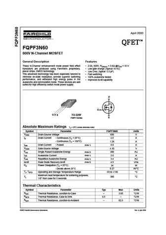
April 2000 TM QFET QFET QFET QFET FQPF3N60 600V N-Channel MOSFET General Description Features These N-Channel enhancement mode power field effect 2.0A, 600V, RDS(on) = 3.6 @VGS = 10 V transistors are produced using Fairchild s proprietary, Low gate charge ( typical 10 nC) planar stripe, DMOS technology. Low Crss ( typical 5.5 pF) This advanced technology has been e
sgp13n60ufd.pdf
IGBT SGP13N60UFD Ultra-Fast IGBT General Description Features Fairchild's UFD series of Insulated Gate Bipolar Transistors High speed switching (IGBTs) provides low conduction and switching losses. Low saturation voltage VCE(sat) = 2.1 V @ IC = 6.5A The UFD series is designed for applications such as motor High input impedance control and general inverters where high spee
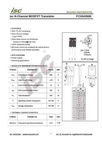
fch043n60.pdf
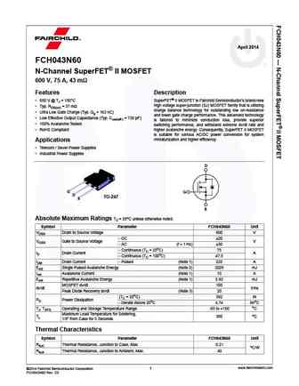
April 2014 FCH043N60 N-Channel SuperFET II MOSFET 600 V, 75 A, 43 m Features Description 650 V @ TJ = 150 C SuperFET II MOSFET is Fairchild Semiconductor s brand-new high voltage super-junction (SJ) MOSFET family that is utilizing Typ. RDS(on) = 37 m charge balance technology for outstanding low on-resistance Ultra Low Gate Charge (Typ. Qg = 163 nC) and lowe
sgf23n60uf.pdf
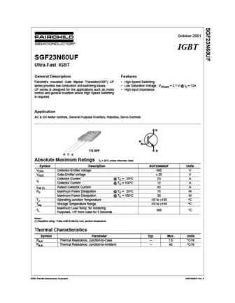
October 2001 IGBT SGF23N60UF Ultra-Fast IGBT General Description Features Fairchild's Insulated Gate Bipolar Transistor(IGBT) UF High Speed Switching series provides low conduction and switching losses. Low Saturation Voltage VCE(sat) = 2.1 V @ IC = 12A UF series is designed for the applications such as motor High Input Impedance control and general inverters where High
fgd3n60lsd.pdf
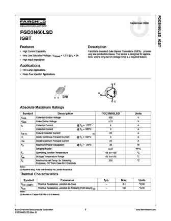
September 2006 FGD3N60LSD tm IGBT Features Description High Current Capability Fairchild's Insulated Gate Bipolar Transistors (IGBTs) provide very low conduction losses. The device is designed for applica- Very Low Saturation Voltage VCE(sat) = 1.2 V @ IC = 3A tions where very low On-Voltage Drop is a required feature. High Input Impedance Applications HID Lamp App
fqb3n60ctm.pdf
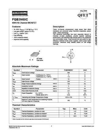
May 2006 TM QFET FQB3N60C 600V N-Channel MOSFET Features Description 3A, 600V, RDS(on) = 3.4 @ VGS = 10 V These N-Channel enhancement mode power field effect transistors are produced using Fairchild s proprietary, planar Low gate charge ( typical 10.5 nC) stripe, DMOS technology. Low Crss ( typical 5 pF) This advanced technology has been especially tailored to
sgw23n60ufd.pdf

N-CHANNEL IGBT SGW23N60UFD FEATURES D2-PAK * High Speed Switching * Low Saturation Voltage VCE(sat) = 1.95 V (@ Ic=12A) * High Input Impedance *CO-PAK, IGBT with FRD Trr = 42nS (typ.) APPLICATIONS C * AC & DC Motor controls * General Purpose Inverters G * Robotics , Servo Controls * Power Supply * Lamp Ballast E ABSOLUTE MAXIMUM RATINGS Symbol Rating Units Characte
sgw13n60ufd.pdf
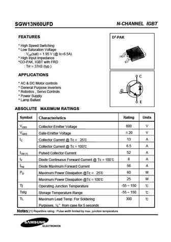
N-CHANNEL IGBT SGW13N60UFD FEATURES D2-PAK * High Speed Switching * Low Saturation Voltage VCE(sat) = 1.95 V (@ Ic=6.5A) * High Input Impedance *CO-PAK, IGBT with FRD Trr = 37nS (typ.) APPLICATIONS C * AC & DC Motor controls * General Purpose Inverters G * Robotics , Servo Controls * Power Supply * Lamp Ballast E ABSOLUTE MAXIMUM RATINGS Symbol Rating Units Charac
sgp23n60uf.pdf
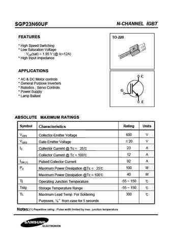
N-CHANNEL IGBT SGP23N60UF FEATURES TO-220 * High Speed Switching * Low Saturation Voltage VCE(sat) = 1.95 V (@ Ic=12A) * High Input Impedance APPLICATIONS C * AC & DC Motor controls * General Purpose Inverters * Robotics , Servo Controls G * Power Supply * Lamp Ballast E ABSOLUTE MAXIMUM RATINGS Symbol Rating Units Characteristics VCES 600 V Collector-Emitter Voltage
sgh13n60ufd.pdf
N-CHANNEL IGBT SGH13N60UFD FEATURES TO-3P * High Speed Switching * Low Saturation Voltage VCE(sat) = 1.95 V (@ Ic=6.5A) * High Input Impedance *CO-PAK, IGBT with FRD Trr = 37nS (typ.) APPLICATIONS C * AC & DC Motor controls * General Purpose Inverters G * Robotics , Servo Controls * Power Supply * Lamp Ballast E ABSOLUTE MAXIMUM RATINGS Symbol Rating Units Charact
sgp13n60uf.pdf

N-CHANNEL IGBT SGP13N60UF FEATURES TO-220 * High Speed Switching * Low Saturation Voltage VCE(sat) = 1.95 V (@ Ic=6.5A) * High Input Impedance APPLICATIONS C * AC & DC Motor controls * General Purpose Inverters * Robotics , Servo Controls G * Power Supply * Lamp Ballast E ABSOLUTE MAXIMUM RATINGS Symbol Rating Units Characteristics VCES 600 V Collector-Emitter Voltage
sgp13n60ufd.pdf
N-CHANNEL IGBT SGP13N60UFD FEATURES TO-220 * High Speed Switching * Low Saturation Voltage VCE(sat) = 1.95 V (@ Ic=6.5A) * High Input Impedance *CO-PAK, IGBT with FRD Trr = 37nS (typ.) APPLICATIONS C * AC & DC Motor controls * General Purpose Inverters G * Robotics , Servo Controls * Power Supply * Lamp Ballast E ABSOLUTE MAXIMUM RATINGS Symbol Rating Units Charac
sgw23n60uf.pdf

N-CHANNEL IGBT SGW23N60UF FEATURES D2-PAK * High Speed Switching * Low Saturation Voltage VCE(sat) = 1.95 V (@ Ic=12A) * High Input Impedance APPLICATIONS C * AC & DC Motor controls * General Purpose Inverters * Robotics , Servo Controls G * Power Supply * Lamp Ballast E ABSOLUTE MAXIMUM RATINGS Symbol Rating Units Characteristics VCES 600 V Collector-Emitter Voltage
sgh23n60uf.pdf

N-CHANNEL IGBT SGH23N60UF FEATURES TO-3P * High Speed Switching * Low Saturation Voltage VCE(sat) = 1.95 V (@ Ic=12A) * High Input Impedance APPLICATIONS C * AC & DC Motor controls * General Purpose Inverters * Robotics , Servo Controls G * Power Supply * Lamp Ballast E ABSOLUTE MAXIMUM RATINGS Symbol Rating Units Characteristics VCES 600 V Collector-Emitter Voltage
sgw13n60uf.pdf
N-CHANNEL IGBT SGW13N60UF FEATURES D2-PAK * High Speed Switching * Low Saturation Voltage VCE(sat) = 1.95 V (@ Ic=6.5A) * High Input Impedance APPLICATIONS C * AC & DC Motor controls * General Purpose Inverters * Robotics , Servo Controls G * Power Supply * Lamp Ballast E ABSOLUTE MAXIMUM RATINGS Symbol Rating Units Characteristics VCES 600 V Collector-Emitter Voltage
sihb33n60e.pdf
SiHB33N60E www.vishay.com Vishay Siliconix E Series Power MOSFET FEATURES PRODUCT SUMMARY Low Figure-of-Merit (FOM) Ron x Qg VDS (V) at TJ max. 650 Low Input Capacitance (Ciss) RDS(on) max. at 25 C ( ) VGS = 10 V 0.099 Reducted Switching and Conduction Losses Qg (Max.) (nC) 150 Ultra Low Gate Charge (Qg) Qgs (nC) 24 Qgd (nC) 42 Avalanche Energy Rated (UIS
sihg33n60ef.pdf

SiHG33N60EF www.vishay.com Vishay Siliconix EF Series Power MOSFET with Fast Body Diode FEATURES PRODUCT SUMMARY Fast body diode MOSFET using E series VDS (V) at TJ max. 650 technology Reduced trr, Qrr, and IRRM RDS(on) max. at 25 C ( ) VGS = 10 V 0.098 Low figure-of-merit (FOM) Ron x Qg Qg (Max.) (nC) 155 Low input capacitance (Ciss) Qgs (nC) 22 Reduced s
sihw33n60e.pdf

SiHW33N60E www.vishay.com Vishay Siliconix E Series Power MOSFET FEATURES PRODUCT SUMMARY Low Figure-of-Merit (FOM) Ron x Qg VDS (V) at TJ max. 650 Low Input Capacitance (Ciss) RDS(on) max. at 25 C ( ) VGS = 10 V 0.099 Reducted Switching and Conduction Losses Qg (Max.) (nC) 150 Ultra Low Gate Charge (Qg) Qgs (nC) 24 Qgd (nC) 42 Avalanche Energy Rated (UIS
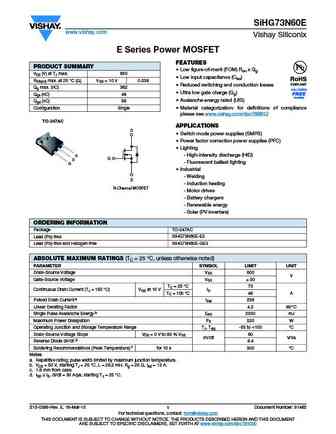
sihw73n60e.pdf
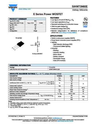
SiHW73N60E www.vishay.com Vishay Siliconix E Series Power MOSFET FEATURES PRODUCT SUMMARY Low figure-of-merit (FOM) Ron x Qg VDS (V) at TJ max. 650 Low input capacitance (Ciss) RDS(on) max. at 25 C ( ) VGS = 10 V 0.039 Reduced switching and conduction losses Qg max. (nC) 362 Ultra low gate charge (Qg) Qgs (nC) 48 Avalanche energy rated (UIS) Qgd (nC) 98 Co
sihp33n60e.pdf
SiHP33N60E www.vishay.com Vishay Siliconix E Series Power MOSFET FEATURES PRODUCT SUMMARY Low Figure-of-Merit (FOM) Ron x Qg VDS (V) at TJ max. 650 Low Input Capacitance (Ciss) RDS(on) max. at 25 C ( ) VGS = 10 V 0.099 Reducted Switching and Conduction Losses Qg (Max.) (nC) 150 Ultra Low Gate Charge (Qg) Qgs (nC) 24 Qgd (nC) 42 Avalanche Energy Rated (UIS
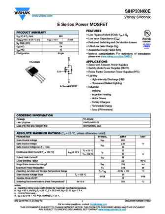
sihb23n60e.pdf
SiHB23N60E www.vishay.com Vishay Siliconix E Series Power MOSFET FEATURES PRODUCT SUMMARY Low figure-of-merit (FOM) Ron x Qg VDS (V) at TJ max. 650 Low input capacitance (Ciss) RDS(on) max. at 25 C ( ) VGS = 10 V 0.158 Reduced switching and conduction losses Qg max. (nC) 95 Ultra low gate charge (Qg) Qgs (nC) 16 Avalanche energy rated (UIS) Qgd (nC) 25
sihg73n60e.pdf
SiHG73N60E www.vishay.com Vishay Siliconix E Series Power MOSFET FEATURES PRODUCT SUMMARY Low figure-of-merit (FOM) Ron x Qg VDS (V) at TJ max. 650 Low input capacitance (Ciss) RDS(on) max. at 25 C ( ) VGS = 10 V 0.039 Reduced switching and conduction losses Qg max. (nC) 362 Ultra low gate charge (Qg) Qgs (nC) 48 Available Avalanche energy rated (UIS) Qgd
sihg33n60e.pdf
SiHG33N60E www.vishay.com Vishay Siliconix E Series Power MOSFET FEATURES PRODUCT SUMMARY Low Figure-of-Merit (FOM) Ron x Qg VDS (V) at TJ max. 650 Low Input Capacitance (Ciss) RDS(on) max. at 25 C ( ) VGS = 10 V 0.099 Reducted Switching and Conduction Losses Qg (Max.) (nC) 150 Ultra Low Gate Charge (Qg) Qgs (nC) 24 Qgd (nC) 42 Avalanche Energy Rated (UIS
sihp23n60e.pdf
SiHP23N60E www.vishay.com Vishay Siliconix E Series Power MOSFET FEATURES PRODUCT SUMMARY Low figure-of-merit (FOM) Ron x Qg VDS (V) at TJ max. 650 Low input capacitance (Ciss) RDS(on) max. at 25 C ( ) VGS = 10 V 0.158 Reduced switching and conduction losses Qg max. (nC) 95 Ultra low gate charge (Qg) Qgs (nC) 16 Qgd (nC) 25 Avalanche energy rated (UIS) Con
sihf23n60e.pdf
SiHF23N60E www.vishay.com Vishay Siliconix E Series Power MOSFET FEATURES PRODUCT SUMMARY Low figure-of-merit (FOM) Ron x Qg VDS (V) at TJ max. 650 Low input capacitance (Ciss) RDS(on) max. at 25 C ( ) VGS = 10 V 0.158 Reduced switching and conduction losses Qg max. (nC) 95 Ultra low gate charge (Qg) Qgs (nC) 16 Qgd (nC) 25 Avalanche energy rated (UIS) Con
sihp33n60ef.pdf
SiHP33N60EF www.vishay.com Vishay Siliconix EF Series Power MOSFET with Fast Body Diode FEATURES PRODUCT SUMMARY Fast body diode MOSFET using E series VDS (V) at TJ max. 650 technology Reduced trr, Qrr, and IRRM RDS(on) max. at 25 C ( ) VGS = 10 V 0.098 Low figure-of-merit (FOM) Ron x Qg Qg (Max.) (nC) 155 Low input capacitance (Ciss) Qgs (nC) 22 Reduced s
sihg23n60e.pdf
SiHG23N60E www.vishay.com Vishay Siliconix E Series Power MOSFET FEATURES PRODUCT SUMMARY Low figure-of-merit (FOM) Ron x Qg VDS (V) at TJ max. 650 Low input capacitance (Ciss) RDS(on) max. at 25 C ( ) VGS = 10 V 0.158 Reduced switching and conduction losses Qg max. (nC) 95 Ultra low gate charge (Qg) Qgs (nC) 16 Avalanche energy rated (UIS) Qgd (nC) 25
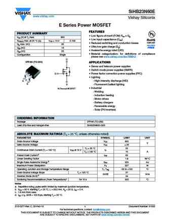
sihb33n60ef.pdf
SiHB33N60EF www.vishay.com Vishay Siliconix EF Series Power MOSFET with Fast Body Diode FEATURES PRODUCT SUMMARY Fast body diode MOSFET using E series VDS (V) at TJ max. 650 technology Reduced trr, Qrr, and IRRM RDS(on) max. at 25 C ( ) VGS = 10 V 0.098 Low figure-of-merit (FOM) Ron x Qg Qg (Max.) (nC) 155 Low input capacitance (Ciss) Qgs (nC) 22 Reduced s
dmg3n60sj3.pdf
DMG3N60SJ3 N-CHANNEL ENHANCEMENT MODE MOSFET Product Summary Features and Benefits Low On-Resistance BV I DSS D R Max DS(ON) (@ T Max) @T = +25 C High BV Rating for Power Application J C DSS Low Input Capacitance 650V 2.8A 3.5 @ V = 10V GS Lead-Free Finish; RoHS Compliant (Notes 1 & 2) Halogen and Antimony Free. Green Device (Note 3)
ikd03n60rf 1 1.pdf
IGBT IGBT with integrated diode in packages offering space saving advantage IKD03N60RF TRENCHSTOPTM RC-Series for hard switching applications up to 30 kHz Datasheet Industrial & Multimarket IKD03N60RF TRENCHSTOPTM RC-Drives Fast Series IGBT with integrated diode in packages offering space saving advantage C Features TRENCHSTOPTM Reverse Conducting (RC) technology for 600V applicat
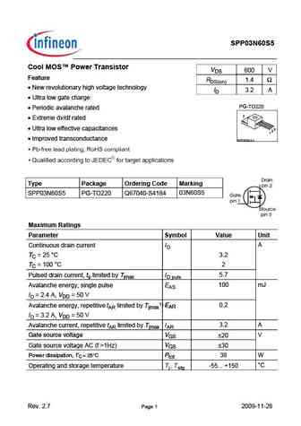
spb03n60s5.pdf
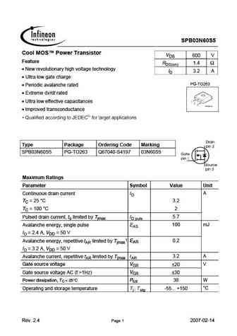
SPB03N60S5 Cool MOS Power Transistor VDS 600 V Feature RDS(on) 1.4 New revolutionary high voltage technology ID 3.2 A Ultra low gate charge PG-TO263 Periodic avalanche rated Extreme dv/dt rated Ultra low effective capacitances Improved transconductance Type Package Ordering Code Marking SPB03N60S5 PG-TO263 Q67040-S4197 03N60S5 Maximum Ratings Para
spd03n60c3 spu03n60c3.pdf
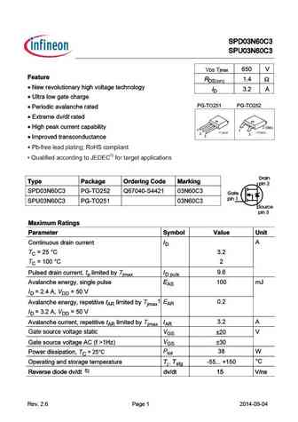
VDS Tjmax 650 V jmax Feature 1.4 DS(on) New revolutionary high voltage technology .2 A D Ultra low gate charge PG TO251 PG TO252 Periodic avalanche rated Extreme dv/dt rated High peak current capability Improved transconductance Type Package Ordering C de Marking SPD0 N60C PG TO252 Q67040 S4421 0 N60C SPU0 N60C PG TO251 0 N60C Maximum Rat
ikd03n60rf.pdf
IGBT IGBT with integrated diode in packages offering space saving advantage IKD03N60RF TRENCHSTOPTM RC-Series for hard switching applications up to 30 kHz Data sheet Industrial Power Control IKD03N60RF TRENCHSTOPTM RC-Drives Fast Series IGBT with integrated diode in packages offering space saving advantage C Features TRENCHSTOPTM Reverse Conducting (RC) technology for 600V applica
spp03n60s5.pdf
SPP03N60S5 Cool MOS Power Transistor VDS 600 V Feature RDS(on) 1.4 New revolutionary high voltage technology ID 3.2 A Ultra low gate charge PG-TO220 Periodic avalanche rated 2 Extreme dv/dt rated Ultra low effective capacitances 3 2 1 Improved transconductance P-TO220-3-1 Type Package Ordering Code Marking 03N60S5 SPP03N60S5 PG-TO220 Q67040-S4
sps03n60c3.pdf
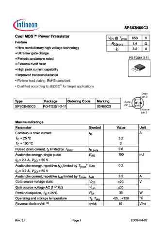
SPS03N60C3 Cool MOS Power Transistor VDS @ Tjmax 650 V Feature RDS(on) 1.4 New revolutionary high voltage technology ID 3.2 A Ultra low gate charge PG-TO251-3-11 Periodic avalanche rated Extreme dv/dt rated High peak current capability Improved transconductance Type Package Ordering Code Marking SPS03N60C3 PG-TO251-3-11 03N60C3 Maximum Ratings Para
spp03n60c3 spa03n60c3 spp03n60c3 spa03n60c3 .pdf
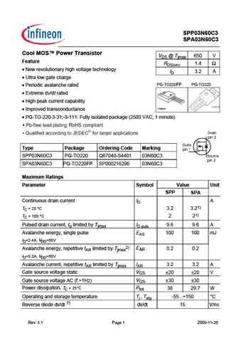
VDS Tjmax G FP G 3 2 1 P-TO220-3-31 G ;-3-111
spd03n60s5 spu03n60s5.pdf
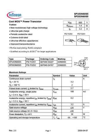
SPU03N60S5 SPD03N60S5 Cool MOS Power Transistor VDS 600 V Feature RDS(on) 1.4 New revolutionary high voltage technology ID 3.2 A Ultra low gate charge PG-TO252 PG-TO251 Periodic avalanche rated Extreme dv/dt rated 2 Ultra low effective capacitances 3 3 1 2 1 Improved transconductance Type Package Ordering Code Marking 03N60S5 SPU03N60S5 PG-T
ixkp13n60c5m.pdf
IXKP 13N60C5M ID25 = 6.5 A CoolMOS 1) Power MOSFET VDSS = 600 V RDS(on) max = 0.3 Fully isolated package N-Channel Enhancement Mode Low RDSon, High VDSS MOSFET D TO-220 FP Ultra low gate charge G D G S Preliminary data S Features MOSFET fast CoolMOS 1) power MOSFET Symbol Conditions Maximum Ratings 4th generation VDSS TVJ = 25 C 600 V - High blocking capabi
ixkc23n60c5.pdf
IXKC 23N60C5 ID25 = 23 A CoolMOS 1) Power MOSFET VDSS = 600 V RDS(on) max = 0.1 Electrically isolated back surface 2500 V electrical isolation N-Channel Enhancement Mode D ISOPLUS220TM Low RDSon, high VDSS MOSFET Ultra low gate charge G G D S isolated back S surface E72873 Preliminary data Features MOSFET Silicon chip on Direct-Copper-Bond Symbol Conditions
ixft23n60q.pdf
IXFH 23N60Q VDSS = 600 V HiPerFETTM IXFT 23N60Q ID25 = 23 A Power MOSFETs RDS(on) = 0.32 Q-Class trr 250ns N-Channel Enhancement Mode Avalanche Rated, High dv/dt, Low Gate Charge and Capacitances Preliminary Data Sheet Symbol Test Conditions Maximum Ratings TO-247 AD (IXFH) VDSS TJ = 25 C to 150 C 600 V VDGR TJ = 25 C to 150 C; R
ixta3n60p ixtp3n60p ixty3n60p.pdf
IXTA 3N60P VDSS = 600 V PolarHVTM IXTP 3N60P ID25 = 3.0 A Power MOSFET IXTY 3N60P RDS(on) 2.9 N-Channel Enhancement Mode Avalanche Rated Symbol Test Conditions Maximum Ratings TO-263 (IXTA) VDSS TJ = 25 C to 150 C 600 V VDGR TJ = 25 C to 150 C; RGS = 1 M 600 V VGS Continuous 30 V G S VGSM Transient 40 V (TAB) ID25 T
hgtd3n60a4s hgtp3n60a4.pdf

Is Now Part of To learn more about ON Semiconductor, please visit our website at www.onsemi.com Please note As part of the Fairchild Semiconductor integration, some of the Fairchild orderable part numbers will need to change in order to meet ON Semiconductor s system requirements. Since the ON Semiconductor product management systems do not have the ability to manage part nomenclatur
fcp13n60n fcpf13n60nt.pdf

Is Now Part of To learn more about ON Semiconductor, please visit our website at www.onsemi.com Please note As part of the Fairchild Semiconductor integration, some of the Fairchild orderable part numbers will need to change in order to meet ON Semiconductor s system requirements. Since the ON Semiconductor product management systems do not have the ability to manage part nomenclatur
fqd3n60ctm-ws.pdf
FQD3N60CTM-WS N-Channel QFET MOSFET Description 600 V, 2.4 A, 3.4 This N-Channel enhancement mode power MOSFET is produced using ON Semiconductor s proprietary planar Features stripe and DMOS technology. This advanced MOSFET 2.4 A, 600 V, RDS(on) = 3.4 (Max.) @ VGS = 10 V, ID = 1.2 A technology has been especially tailored to reduce on-state resistance, and to pro
ndf03n60z ndp03n60z ndd03n60z.pdf
NDF03N60Z, NDP03N60Z, NDD03N60Z N-Channel Power MOSFET 600 V, 3.3 W Features http //onsemi.com Low ON Resistance Low Gate Charge 100% Avalanche Tested VDSS RDS(on) (TYP) @ 1.2 A These Devices are Pb-Free and are RoHS Compliant 600 V 3.3 W ABSOLUTE MAXIMUM RATINGS (TC = 25 C unless otherwise noted) Rating Symbol NDF NDP NDD Unit N-Channel D (2) Drain-to-Source V
fgd3n60undf.pdf

Is Now Part of To learn more about ON Semiconductor, please visit our website at www.onsemi.com Please note As part of the Fairchild Semiconductor integration, some of the Fairchild orderable part numbers will need to change in order to meet ON Semiconductor s system requirements. Since the ON Semiconductor product management systems do not have the ability to manage part nomenclatur
fch043n60.pdf

Is Now Part of To learn more about ON Semiconductor, please visit our website at www.onsemi.com Please note As part of the Fairchild Semiconductor integration, some of the Fairchild orderable part numbers will need to change in order to meet ON Semiconductor s system requirements. Since the ON Semiconductor product management systems do not have the ability to manage part nomenclatur
sgf23n60uf.pdf

Is Now Part of To learn more about ON Semiconductor, please visit our website at www.onsemi.com Please note As part of the Fairchild Semiconductor integration, some of the Fairchild orderable part numbers will need to change in order to meet ON Semiconductor s system requirements. Since the ON Semiconductor product management systems do not have the ability to manage part nomenclatur
fgd3n60lsd.pdf
FGD3N60LSD IGBT Description ON Semiconductor's Insulated Gate Bipolar Transistors Features (IGBTs) provide very low conduction losses. The device is High Current Capability designed for applica-tions where very low On-Voltage Drop is a required feature. Very Low Saturation Voltage VCE(sat) = 1.2 V @ IC = 3A High Input Impedance Applications HID Lamp Applications
fqp3n60c.pdf

Is Now Part of To learn more about ON Semiconductor, please visit our website at www.onsemi.com Please note As part of the Fairchild Semiconductor integration, some of the Fairchild orderable part numbers will need to change in order to meet ON Semiconductor s system requirements. Since the ON Semiconductor product management systems do not have the ability to manage part nomenclatur
ngtb03n60r2dt4g.pdf
NGTB03N60R2DT4G IGBT 600V, 4.5A, N-Channel www.onsemi.com Features Electrical Connection Reverse Conducting II IGBT N-Channel IGBT VCE(sat)=1.7V (typ) [IC=3A, VGE=15V] 2,4 IGBT tf=75ns (typ) Diode VF=1.5V (typ) [IF=3A] Diode trr=65ns (typ) 5 s Short Circuit Capability 1 1 Gate 2 Collector Applications 3 Emitter 3 General Pur
3n60k.pdf
UNISONIC TECHNOLOGIES CO., LTD 3N60K Power MOSFET 3A, 600V N-CHANNEL POWER MOSFET DESCRIPTION The UTC 3N60K is a high voltage and high current power MOSFET , designed to have better characteristics, such as fast switching time, low gate charge, low on-state resistance and have a high rugged avalanche characteristics. This power MOSFET is usually used at high speed switching
3n60a.pdf
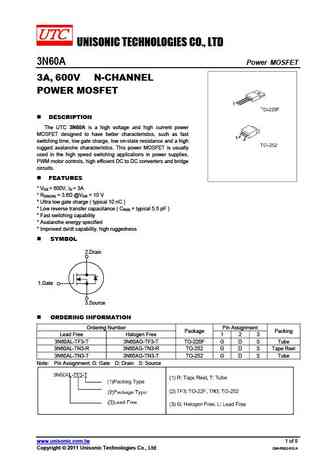
UNISONIC TECHNOLOGIES CO., LTD 3N60A Power MOSFET 3A, 600V N-CHANNEL POWER MOSFET DESCRIPTION The UTC 3N60A is a high voltage and high current power MOSFET designed to have better characteristics, such as fast switching time, low gate charge, low on-state resistance and a high rugged avalanche characteristics. This power MOSFET is usually used in the high speed switching app
3n60z.pdf
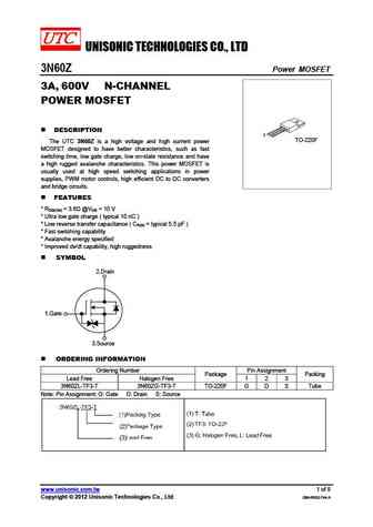
UNISONIC TECHNOLOGIES CO., LTD 3N60Z Power MOSFET 3A, 600V N-CHANNEL POWER MOSFET DESCRIPTION 1 TO-220F The UTC 3N60Z is a high voltage and high current power MOSFET designed to have better characteristics, such as fast switching time, low gate charge, low on-state resistance and have a high rugged avalanche characteristics. This power MOSFET is usually used at high speed
fmc03n60e.pdf
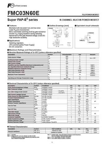
FMC03N60E FUJI POWER MOSFET Super FAP-E3 series N-CHANNEL SILICON POWER MOSFET Features Outline Drawings [mm] Equivalent circuit schematic Maintains both low power loss and low noise T-Pack(S) Lower R (on) characteristic DS More controllable switching dv/dt by gate resistance Drain(D) Smaller V ringing waveform during switching GS Narrow band of the gate threshold voltage (3.0 0.5V)
fmv13n60es.pdf

FMV13N60ES FUJI POWER MOSFET Super FAP-E3S series N-CHANNEL SILICON POWER MOSFET Features Outline Drawings [mm] Equivalent circuit schematic Maintains both low power loss and low noise TO-220F(SLS) Lower R (on) characteristic DS More controllable switching dv/dt by gate resistance Drain(D) Smaller V ringing waveform during switching GS Narrow band of the gate threshold voltage (4.2
fmc13n60es.pdf

FMC13N60ES FUJI POWER MOSFET Super FAP-E3S series N-CHANNEL SILICON POWER MOSFET Features Outline Drawings [mm] Equivalent circuit schematic Maintains both low power loss and low noise T-Pack(S) Lower R (on) characteristic DS More controllable switching dv/dt by gate resistance Drain(D) Smaller V ringing waveform during switching GS Narrow band of the gate threshold voltage (4.2 0.5
fmr23n60e.pdf
FMR23N60E FUJI POWER MOSFET Super FAP-E3 series N-CHANNEL SILICON POWER MOSFET Features Outline Drawings [mm] Equivalent circuit schematic Maintains both low power loss and low noise TO-3PF Lower R (on) characteristic DS More controllable switching dv/dt by gate resistance Drain(D) Smaller V ringing waveform during switching GS Narrow band of the gate threshold voltage (3.0 0.5V) H
fmh23n60es.pdf
FMH23N60ES FUJI POWER MOSFET Super FAP-E3S series N-CHANNEL SILICON POWER MOSFET Features Outline Drawings [mm] Equivalent circuit schematic Maintains both low power loss and low noise TO-3P(Q) Lower R (on) characteristic DS More controllable switching dv/dt by gate resistance Drain(D) Smaller V ringing waveform during switching GS Narrow band of the gate threshold voltage (4.2 0.5V
fmc13n60e.pdf

FMC13N60E FUJI POWER MOSFET Super FAP-E3 series N-CHANNEL SILICON POWER MOSFET Features Outline Drawings [mm] Equivalent circuit schematic Maintains both low power loss and low noise T-Pack(S) Lower R (on) characteristic DS More controllable switching dv/dt by gate resistance Drain(D) Smaller V ringing waveform during switching GS Narrow band of the gate threshold voltage (3.0 0.5V)
fmp03n60e.pdf

FMP03N60E FUJI POWER MOSFET Super FAP-E3 series N-CHANNEL SILICON POWER MOSFET Features Outline Drawings [mm] Equivalent circuit schematic Maintains both low power loss and low noise TO-220AB Lower R (on) characteristic DS More controllable switching dv/dt by gate resistance Drain(D) Smaller V ringing waveform during switching GS Narrow band of the gate threshold voltage (3.0 0.5V)
fmh13n60es.pdf
FMH13N60ES FUJI POWER MOSFET Super FAP-E3S series N-CHANNEL SILICON POWER MOSFET Features Outline Drawings [mm] Equivalent circuit schematic Maintains both low power loss and low noise TO-3P(Q) Lower R (on) characteristic DS More controllable switching dv/dt by gate resistance Drain(D) Smaller V ringing waveform during switching GS Narrow band of the gate threshold voltage (4.2 0.5V
fmi03n60e.pdf

FMI03N60E FUJI POWER MOSFET Super FAP-E3 series N-CHANNEL SILICON POWER MOSFET Features Outline Drawings [mm] Equivalent circuit schematic Maintains both low power loss and low noise T-Pack(L) Lower R (on) characteristic DS More controllable switching dv/dt by gate resistance Drain(D) Smaller V ringing waveform during switching GS Narrow band of the gate threshold voltage (3.0 0.5V)
fmr23n60es.pdf
FMR23N60ES FUJI POWER MOSFET Super FAP-E3S series N-CHANNEL SILICON POWER MOSFET Features Outline Drawings [mm] Equivalent circuit schematic Maintains both low power loss and low noise TO-3PF Lower R (on) characteristic DS More controllable switching dv/dt by gate resistance Drain(D) Smaller V ringing waveform during switching GS Narrow band of the gate threshold voltage (4.2 0.5V)
fmv13n60e.pdf

FMV13N60E FUJI POWER MOSFET Super FAP-E3 series N-CHANNEL SILICON POWER MOSFET Features Outline Drawings [mm] Equivalent circuit schematic Maintains both low power loss and low noise TO-220F(SLS) Lower R (on) characteristic DS More controllable switching dv/dt by gate resistance Drain(D) Smaller V ringing waveform during switching GS Narrow band of the gate threshold voltage (3.0 0.
fmi13n60e.pdf
FMI13N60E FUJI POWER MOSFET Super FAP-E3 series N-CHANNEL SILICON POWER MOSFET Features Outline Drawings [mm] Equivalent circuit schematic Maintains both low power loss and low noise T-Pack(L) Lower R (on) characteristic DS More controllable switching dv/dt by gate resistance Drain(D) Smaller V ringing waveform during switching GS Narrow band of the gate threshold voltage (3.0 0.5V)
fmi13n60es.pdf
FMI13N60ES FUJI POWER MOSFET Super FAP-E3S series N-CHANNEL SILICON POWER MOSFET Features Outline Drawings [mm] Equivalent circuit schematic Maintains both low power loss and low noise T-Pack(L) Lower R (on) characteristic DS More controllable switching dv/dt by gate resistance Drain(D) Smaller V ringing waveform during switching GS Narrow band of the gate threshold voltage (
fmp13n60e.pdf

FMP13N60E FUJI POWER MOSFET Super FAP-E3 series N-CHANNEL SILICON POWER MOSFET Features Outline Drawings [mm] Equivalent circuit schematic Maintains both low power loss and low noise TO-220AB Lower R (on) characteristic DS More controllable switching dv/dt by gate resistance Drain(D) Smaller V ringing waveform during switching GS Narrow band of the gate threshold voltage (3.0 0.5V)
fmp13n60es.pdf
FMP13N60ES FUJI POWER MOSFET Super FAP-E3S series N-CHANNEL SILICON POWER MOSFET Features Outline Drawings [mm] Equivalent circuit schematic Maintains both low power loss and low noise TO-220AB Lower R (on) characteristic DS More controllable switching dv/dt by gate resistance Drain(D) Smaller V ringing waveform during switching GS Narrow band of the gate threshold voltage (4.2 0.5
fmv03n60e.pdf

FMV03N60E FUJI POWER MOSFET Super FAP-E3 series N-CHANNEL SILICON POWER MOSFET Features Outline Drawings [mm] Equivalent circuit schematic Maintains both low power loss and low noise TO-220F(SLS) Lower R (on) characteristic DS More controllable switching dv/dt by gate resistance Drain(D) Smaller V ringing waveform during switching GS Narrow band of the gate threshold voltage (3.0 0.
fmh23n60e.pdf
FMH23N60E FUJI POWER MOSFET Super FAP-E3 series N-CHANNEL SILICON POWER MOSFET Features Outline Drawings [mm] Equivalent circuit schematic Maintains both low power loss and low noise TO-3P(Q) Lower R (on) characteristic DS More controllable switching dv/dt by gate resistance Drain(D) Smaller V ringing waveform during switching GS Narrow band of the gate threshold voltage (3.0 0.5V)
fml13n60es.pdf
http //www.fujisemi.com FML13N60ES FUJI POWER MOSFET Super FAP-E3 series N-CHANNEL SILICON POWER MOSFET Features Outline Drawings [mm] Equivalent circuit schematic Maintains both low power loss and low noise TFP 9.0 0.2 7.0 0.2 0.4 0.1 Lower R (on) characteristic DS 4 More controllable switching dv/dt by gate resistance 4 D Smaller V ringing waveform during switching GS Narrow
hgtd3n60.pdf
HGTD3N60C3, S E M I C O N D U C T O R HGTD3N60C3S June 1996 6A, 600V, UFS Series N-Channel IGBT Features Packaging JEDEC TO-251AA 6A, 600V at TC = +25oC 600V Switching SOA Capability EMITTER COLLECTOR Typical Fall Time - 130ns at TJ = +150oC GATE Short Circuit Rating Low Conduction Loss COLLECTOR (FLANGE) Description The HGTD3N60C3 and HGTD3N60C3S are MOS ga

kf13n60n.pdf
KF13N60N SEMICONDUCTOR N CHANNEL MOS FIELD TECHNICAL DATA EFFECT TRANSISTOR General Description A This planar stripe MOSFET has better characteristics, such as fast Q B N O K switching time, low on resistance, low gate charge and excellent DIM MILLIMETERS avalanche characteristics. It is mainly suitable for switching mode _ A + 15.60 0.20 _ B 4.80 + 0.20 power supplies. _
kf3n60d-i.pdf
KF3N60D/I SEMICONDUCTOR N CHANNEL MOS FIELD TECHNICAL DATA EFFECT TRANSISTOR General Description KF3N60D This planar stripe MOSFET has better characteristics, such as fast switching time, low on resistance, low gate charge and excellent A K DIM MILLIMETERS avalanche characteristics. It is mainly suitable for electronic ballast and L C D _ A 6.60 + 0.20 switching mode power supp
kf3n60p-f.pdf
KF3N60P/F SEMICONDUCTOR N CHANNEL MOS FIELD TECHNICAL DATA EFFECT TRANSISTOR General Description KF3N60P A This planar stripe MOSFET has better characteristics, such as fast O C switching time, low on resistance, low gate charge and excellent F avalanche characteristics. It is mainly suitable for electronic ballast and E DIM MILLIMETERS G _ switching mode power supplies. A 9.9
apt53n60bc6 apt53n60sc6.pdf
APT53N60BC6 APT53N60SC6 600V 53A 0.070 COOLMOS Power Semiconductors Super Junction MOSFET Ultra Low RDS(ON) D3PAK Low Miller Capacitance Ultra Low Gate Charge, Qg Avalanche Energy Rated Extreme dv/dt Rated D Popular TO-247 or Surface Mount D3 package. G S MAXIMUM RATINGS All Ratings per die TC = 25 C unless otherwise specified. Symbol Parame
h03n60.pdf
Spec. No. MOS200602 HI-SINCERITY Issued Date 2006.02.01 Revised Date 2006.02.07 MICROELECTRONICS CORP. Page No. 1/5 H03N60 Series Pin Assignment H03N60 Series Tab N-Channel Power Field Effect Transistor 3-Lead Plastic TO-220AB Package Code E Pin 1 Gate Pin 2 & Tab Drain Description Pin 3 Source 3 This high voltage MOSFET uses an advanced termination scheme to 2 1
aod3n60.pdf
AOD3N60/AOU3N60 600V,2.5A N-Channel MOSFET General Description Product Summary The AOD3N60 & AOU3N60 have been fabricated using an advanced high voltage MOSFET process that is VDS 700V@150 designed to deliver high levels of performance and ID (at VGS=10V) 2.5A robustness in popular AC-DC applications. RDS(ON) (at VGS=10V)
aot3n60.pdf
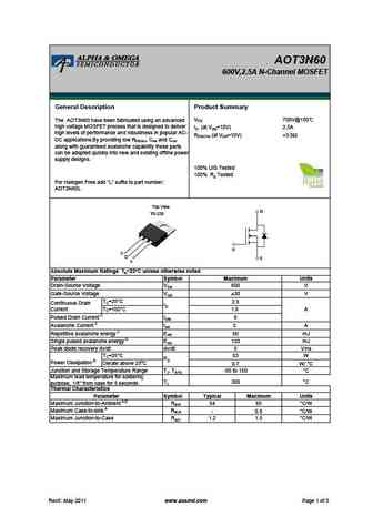
AOT3N60 600V,2.5A N-Channel MOSFET General Description Product Summary VDS 700V@150 The AOT3N60 have been fabricated using an advanced high voltage MOSFET process that is designed to deliver ID (at VGS=10V) 2.5A high levels of performance and robustness in popular AC- RDS(ON) (at VGS=10V)
aou3n60.pdf

AOD3N60/AOU3N60 600V,2.5A N-Channel MOSFET General Description Product Summary The AOD3N60 & AOU3N60 have been fabricated using an advanced high voltage MOSFET process that is VDS 700V@150 designed to deliver high levels of performance and ID (at VGS=10V) 2.5A robustness in popular AC-DC applications. RDS(ON) (at VGS=10V)
aod3n60 aou3n60.pdf

AOD3N60/AOU3N60 600V,2.5A N-Channel MOSFET General Description Product Summary The AOD3N60 & AOU3N60 have been fabricated using an advanced high voltage MOSFET process that is VDS 700V@150 designed to deliver high levels of performance and ID (at VGS=10V) 2.5A robustness in popular AC-DC applications. RDS(ON) (at VGS=10V)
sff23n60s1 sff23n60s2.pdf
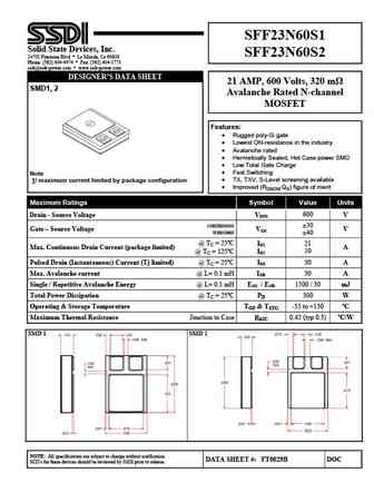
SFF23N60S1 Solid State Devices, Inc. SFF23N60S2 14701 Firestone Blvd * La Mirada, Ca 90638 Phone (562) 404-4474 * Fax (562) 404-1773 ssdi@ssdi-power.com * www.ssdi-power.com DESIGNER S DATA SHEET 21 AMP, 600 Volts, 320 m SMD1, 2 Avalanche Rated N-channel MOSFET Features Rugged poly-Si gate Lowest ON-resistance in the industry Avalanche rated
sff23n60m sff23n60z.pdf
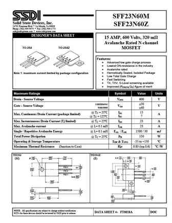
SFF23N60M Solid State Devices, Inc. SFF23N60Z 14701 Firestone Blvd * La Mirada, Ca 90638 Phone (562) 404-4474 * Fax (562) 404-1773 ssdi@ssdi-power.com * www.ssdi-power.com DESIGNER S DATA SHEET 15 AMP, 600 Volts, 320 m Avalanche Rated N-channel TO-254 TO-254Z MOSFET Features Advanced low gate charge process Lowest ON-resistance in the industry Av
mtn3n60i3.pdf
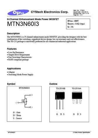
Spec. No. C798I3 Issued Date 2010.08.12 CYStech Electronics Corp. Revised Date 2011.11.10 Page No. 1/11 N-Channel Enhancement Mode Power MOSFET BVDSS 600V RDS(ON) 3.6 (typ.) MTN3N60I3 ID 3A Description The MTN3N60I3 is a N-channel enhancement-mode MOSFET, providing the designer with the best combination of fast switching, ruggedized device design, low on-r
mtn3n60j3.pdf
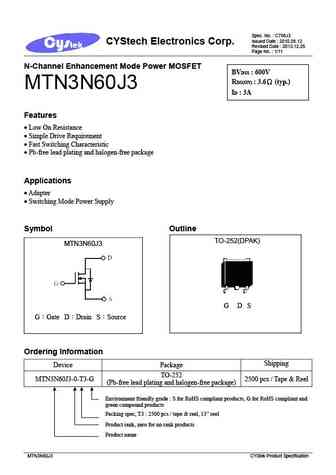
Spec. No. C798J3 Issued Date 2010.08.12 CYStech Electronics Corp. Revised Date 2013.12.26 Page No. 1/11 N-Channel Enhancement Mode Power MOSFET BVDSS 600V RDS(ON) 3.6 (typ.) MTN3N60J3 ID 3A Features Low On Resistance Simple Drive Requirement Fast Switching Characteristic Pb-free lead plating and halogen-free package Applications
mtn3n60fp.pdf
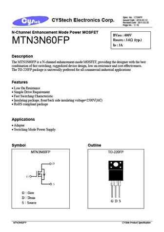
Spec. No. C798FP Issued Date 2010.03.12 CYStech Electronics Corp. Revised Date 2011.03.30 Page No. 1/ 10 N-Channel Enhancement Mode Power MOSFET BVDSS 600V RDS(ON) 3.6 (typ.) MTN3N60FP ID 3A Description The MTN3N60FP is a N-channel enhancement-mode MOSFET, providing the designer with the best combination of fast switching, ruggedized device design, low on-
13n60a 13n60af.pdf
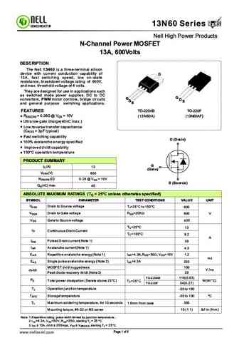
RoHS 13N60 Series RoHS SEMICONDUCTOR Nell High Power Products N-Channel Power MOSFET 13A, 600Volts DESCRIPTION The Nell 13N60 is a three-terminal silicon device with current conduction capability of D 13A, fast switching speed, low on-state resistance, breakdown voltage rating of 600V, and max. threshold voltage of 4 volts. They are designed for use in applications such as s
3n60af 3n60f 3n60g.pdf
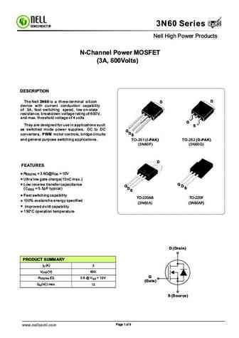
RoHS 3N60 Series RoHS SEMICONDUCTOR Nell High Power Products N-Channel Power MOSFET (3A, 600Volts) DESCRIPTION D The Nell 3N60 is a three-terminal silicon D device with current conduction capability of 3A, fast switching speed, low on-state resistance, breakdown voltage rating of 600V, and max. threshold voltage of 4 volts. G They are designed for use in applications such
cs3n60 a3.pdf
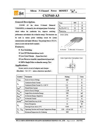
Silicon N-Channel Power MOSFET R CS3N60 A3 General Description VDSS 600 V CS3N60 A3 the silicon N-channel Enhanced ID 3 A PD (TC=25 ) 55 W VDMOSFETs, is obtained by the self-aligned planar Technology RDS(ON)Typ 2.7 which reduce the conduction loss, improve switching performance and enhance the avalanche energy. The transistor can be used in various power swit
jfpc13n60ci.pdf
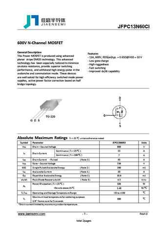
JFPC13N60CI 600V N-Channel MOSFET General Description Features This Power MOSFET is produced using advanced - 13A, 600V, RDS(on)typ. = 0.65 @VGS = 10 V planar stripe DMOS technology. This advanced - Low gate charge technology has been especially tailored to minimize - High ruggedness on-state resistance, provide superior switching - Fast switching performance, and withs
ptp13n60 pta13n60.pdf
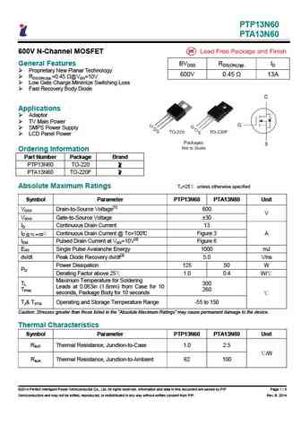
PTP13N60 PTA13N60 600V N-Channel MOSFET General Features BVDSS RDS(ON),typ. ID Proprietary New Planar Technology 600V 0.45 13A RDS(ON),typ.=0.45 @VGS=10V Low Gate Charge Minimize Switching Loss Fast Recovery Body Diode Applications Adaptor TV Main Power SMPS Power Supply LCD Panel Power Ordering Information Part Number Package Brand PTP13N60 TO-22
swf13n60d.pdf
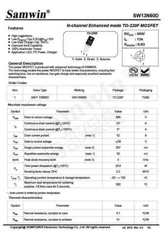
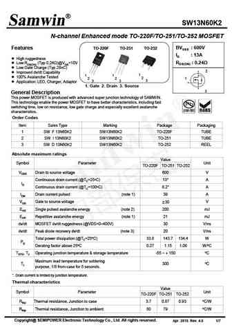
SW13N60D N-channel Enhanced mode TO-220F MOSFET Features TO-220F BVDSS 600V High ruggedness Low RDS(ON) (Typ 0.5 )@VGS=10V ID 13A Low Gate Charge (Typ 54nC) RDS(ON) 0.5 Improved dv/dt Capability 100% Avalanche Tested 2 1 Application LED, PC Power, Charger 2 3 1 1. Gate 2. Drain 3. Source General Description 3 This pow
swf13n60k2 swi13n60k2 swd13n60k2.pdf
SW13N60K2 N-channel Enhanced mode TO-220F/TO-251/TO-252 MOSFET BVDSS 600V Features TO-220F TO-251 TO-252 ID 13A High ruggedness RDS(ON) 0.24 Low RDS(ON) (Typ 0.24 )@VGS=10V Low Gate Charge (Typ 28nC) 2 Improved dv/dt Capability 1 1 1 100% Avalanche Tested 2 2 2 1 3 3 3 Application LED, Charger, Adaptor 1. Gate 2. Drain 3
hfs13n60u.pdf
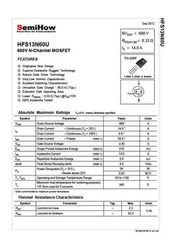
Sep 2012 BVDSS = 600 V RDS(on) typ = 0.33 HFS13N60U ID = 14.0 A 600V N-Channel MOSFET TO-220F FEATURES Originative New Design Superior Avalanche Rugged Technology 1 2 3 Robust Gate Oxide Technology 1.Gate 2. Drain 3. Source Very Low Intrinsic Capacitances Excellent Switching Characteristics Unrivalled Gate Charge 60.0 nC (Typ.) Extended Safe Operating Area
hfp13n60u.pdf
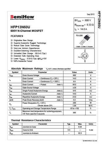
Sep 2012 BVDSS = 600 V RDS(on) typ = 0.33 HFP13N60U ID = 14.0 A 600V N-Channel MOSFET TO-220 FEATURES Originative New Design Superior Avalanche Rugged Technology 1 2 3 Robust Gate Oxide Technology 1.Gate 2. Drain 3. Source Very Low Intrinsic Capacitances Excellent Switching Characteristics Unrivalled Gate Charge 60.0 nC (Typ.) Extended Safe Operating Area
wml53n60c4 wmk53n60c4 wmn53n60c4 wmm53n60c4 wmj53n60c4.pdf

WML53N MK53N60C N60C4, WM C4 WMN53N60C4, WMM53N MJ53N60C N60C4, WM C4 600V 0.06 S unction Power M T Super Ju MOSFET Descrip ption WMOSTM C4 is Wa 4th generation super ayon s n junction MOSFET fa that is utilizing charge M amily S balance te or extremely esistance echnology fo y low on-re S D D G G G S D G and low ga charge performanc WMOSTM C4 is ate
wml53n60f2 wmk53n60f2 wmn53n60f2 wmm53n60f2 wmj53n60f2.pdf
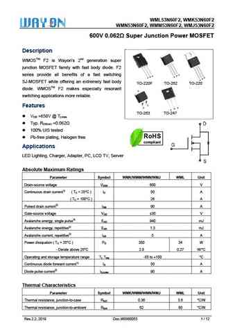
WML53N MK53N60F N60F2, WM F2 WMN , WMM53N MJ53N60F N53N60F2, N60F2, WM F2 600V 0.062 S 0 Super Junction Power MOSFET Descrip ption WMOSTM F2 is Wa 2nd generation super ayon s n junction MOSFET fam with fa body di F2 M mily ast iode. S series pro all benefits of a fast switching ovide b f s S D D G G G S D G SJ-MOSFE while of an extremely fa body ET f
cs3n60a3.pdf

Silicon N-Channel Power MOSFET R CS3N60 A3 General Description VDSS 600 V CS3N60 A3 the silicon N-channel Enhanced ID 3 A PD (TC=25 ) 55 W VDMOSFETs, is obtained by the self-aligned planar Technology RDS(ON)Typ 2.7 which reduce the conduction loss, improve switching performance and enhance the avalanche energy. The transistor can be used in various power swit
cs13n60p cs13n60f.pdf
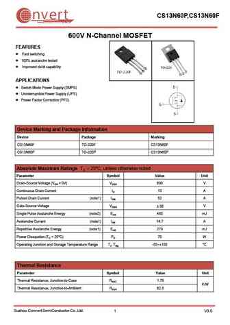
CS13N60P,CS13N60F nvert Suzhou Convert Semiconductor Co ., Ltd. 600V N-Channel MOSFET FEATURES Fast switching 100% avalanche tested Improved dv/dt capability APPLICATIONS Switch Mode Power Supply (SMPS) Uninterruptible Power Supply (UPS) Power Factor Correction (PFC) Device Marking and Package Information Device Package Marking CS13N60F TO-220F CS13N60F CS
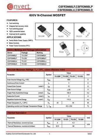
csfr3n60lf csfr3n60lp csfr3n60lu csfr3n60ld.pdf
CSFR3N60LF,CSFR3N60LP nvert Suzhou Convert Semiconductor Co ., Ltd. CSFR3N60LU,CSFR3N60LD 600V N-Channel MOSFET FEATURES Fast switching Integrate fast recovery diode Fast switching speed 100% avalanche tested Improved dv/dt capability APPLICATIONS Switch Mode Power Supply (SMPS) Motor Controls Power Factor Correction (PFC) Device Marking and Packag
csfr3n60f csfr3n60p csfr3n60u csfr3n60d.pdf
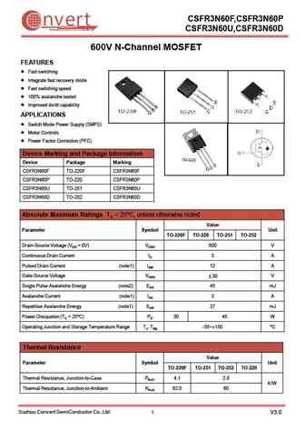
CSFR3N60F,CSFR3N60P nvert Suzhou Convert Semiconductor Co ., Ltd. CSFR3N60U,CSFR3N60D 600V N-Channel MOSFET FEATURES Fast switching Integrate fast recovery diode Fast switching speed 100% avalanche tested Improved dv/dt capability APPLICATIONS Switch Mode Power Supply (SMPS) Motor Controls Power Factor Correction (PFC) Device Marking and Package In
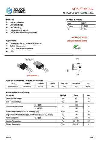
sfp053n60c2.pdf
SFP053N60C2 N-MOSFET 60V, 4.3m , 140A Features Product Summary Low on resistance V 60V DS Low gate charge R 4.3m DS(on) Fast switching I 140A D High avalanche current Low reverse transfer capacitances 100% DVDS Tested Application 100% Avalanche Tested Brushed and BLDC Motor drive systems Battery Management DC/DC and AC/DC Converter
mpto3n60.pdf
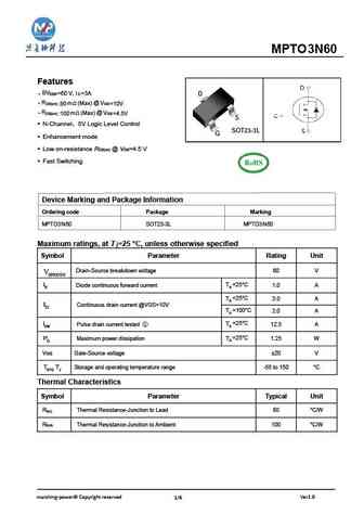
MPTO3N60 Features BV DSS=60 V, I D =3A D @ RDS(on) m (Max) V 80 GS=10V @ RDS(on) m (Max) V 100 GS=4.5V S N-Channel 5V Logic Level Control SOT23-3L G Enhancement mode Low on-resistance RDS(on) @ VGS=4.5 V Fast Switching Device Marking and Package Information Ordering code Package Marking MPTO3N60 SOT23-3L MPTO3N60 Maximum ratings,
spb03n60c3.pdf
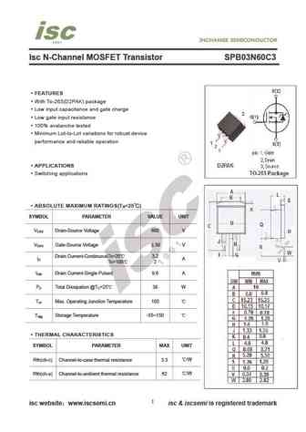
Isc N-Channel MOSFET Transistor SPB03N60C3 FEATURES With To-263(D2PAK) package Low input capacitance and gate charge Low gate input resistance 100% avalanche tested Minimum Lot-to-Lot variations for robust device performance and reliable operation APPLICATIONS Switching applications ABSOLUTE MAXIMUM RATINGS(T =25 ) a SYMBOL PARAMETER VALUE UNIT V Drain-Source Vo
aod3n60.pdf
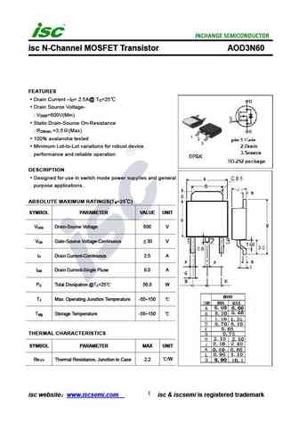
isc N-Channel MOSFET Transistor AOD3N60 FEATURES Drain Current I = 2.5A@ T =25 D C Drain Source Voltage- V =600V(Min) DSS Static Drain-Source On-Resistance R =3.5 (Max) DS(on) 100% avalanche tested Minimum Lot-to-Lot variations for robust device performance and reliable operation DESCRIPTION Designed for use in switch mode power supplies and general purpose
fmr23n60e.pdf
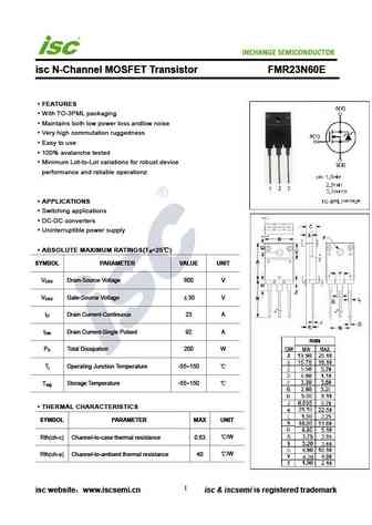
INCHANGE Semiconductor isc N-Channel MOSFET Transistor FMR23N60E FEATURES With TO-3PML packaging Maintains both low power loss andlow noise Very high commutation ruggedness Easy to use 100% avalanche tested Minimum Lot-to-Lot variations for robust device performance and reliable operationz APPLICATIONS Switching applications DC-DC converters Uninterruptible po
dmg3n60sct.pdf
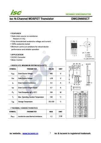
isc N-Channel MOSFET Transistor DMG3N60SCT FEATURES Static drain-source on-resistance RDS(on) 3.5 Fully characterized avalanche voltage and current 100% avalanche tested Minimum Lot-to-Lot variations for robust device performance and reliable operation APPLICATION DC/DC Converter Motor Control ABSOLUTE MAXIMUM RATINGS(T =25 ) a SYMBOL PARAMETER VALUE UNI
aot3n60.pdf
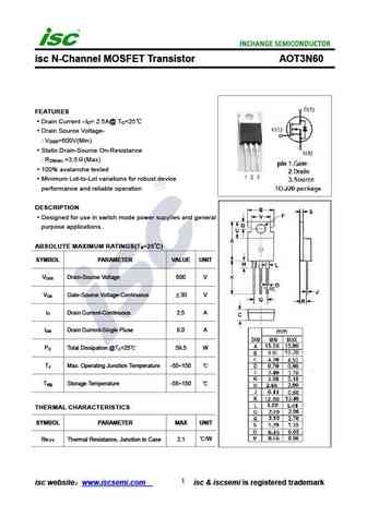
isc N-Channel MOSFET Transistor AOT3N60 FEATURES Drain Current I = 2.5A@ T =25 D C Drain Source Voltage- V =600V(Min) DSS Static Drain-Source On-Resistance R =3.5 (Max) DS(on) 100% avalanche tested Minimum Lot-to-Lot variations for robust device performance and reliable operation DESCRIPTION Designed for use in switch mode power supplies and general purpose
spd03n60c3.pdf
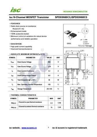
isc N-Channel MOSFET Transistor SPD03N60C3,ISPD03N60C3 FEATURES Static drain-source on-resistance RDS(on) 1.4 Enhancement mode 100% avalanche tested Minimum Lot-to-Lot variations for robust device performance and reliable operation DESCRITION High peak current capability Improved transconductance ABSOLUTE MAXIMUM RATINGS(T =25 ) a SYMBOL PARAMETER VALUE U
spu03n60s5.pdf
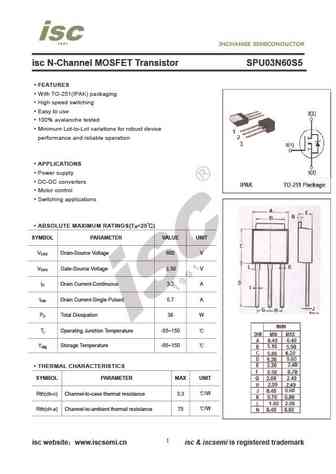
isc N-Channel MOSFET Transistor SPU03N60S5 FEATURES With TO-251(IPAK) packaging High speed switching Easy to use 100% avalanche tested Minimum Lot-to-Lot variations for robust device performance and reliable operation APPLICATIONS Power supply DC-DC converters Motor control Switching applications ABSOLUTE MAXIMUM RATINGS(T =25 ) a SYMBOL PARAMETER VALUE
spd03n60s5.pdf
isc N-Channel MOSFET Transistor SPD03N60S5,ISPD03N60S5 FEATURES Static drain-source on-resistance RDS(on) 1.4 Enhancement mode 100% avalanche tested Minimum Lot-to-Lot variations for robust device performance and reliable operation DESCRITION Improved transconductance ABSOLUTE MAXIMUM RATINGS(T =25 ) a SYMBOL PARAMETER VALUE UNIT V Drain-Source Voltage 600
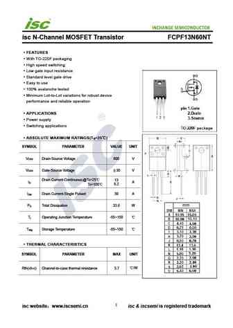
fcp13n60n.pdf
isc N-Channel MOSFET Transistor FCP13N60N FEATURES With TO-220 packaging High speed switching Low gate input resistance Standard level gate drive Easy to use 100% avalanche tested Minimum Lot-to-Lot variations for robust device performance and reliable operation APPLICATIONS Power supply Switching applications ABSOLUTE MAXIMUM RATINGS(T =25 ) a SYMBOL PA
spp03n60s5.pdf
isc N-Channel MOSFET Transistor SPP03N60S5 ISPP03N60S5 FEATURES Static drain-source on-resistance RDS(on) 1.4 Enhancement mode Fast Switching Speed 100% avalanche tested Minimum Lot-to-Lot variations for robust device performance and reliable operation DESCRIPTION Ultra low gate charge Ultra low effective capacitance Improved transconductance ABSOLUTE
spu03n60c3.pdf

isc N-Channel MOSFET Transistor SPU03N60C3 FEATURES With TO-251(IPAK) packaging High speed switching Easy to use 100% avalanche tested Minimum Lot-to-Lot variations for robust device performance and reliable operation APPLICATIONS Power supply DC-DC converters Motor control Switching applications ABSOLUTE MAXIMUM RATINGS(T =25 ) a SYMBOL PARAMETER VALUE
apt53n60bc6.pdf
isc N-Channel MOSFET Transistor APT53N60BC6 FEATURES Drain Current I =53A@ T =25 D C Drain Source Voltage- V =600V(Min) DSS Static Drain-Source On-Resistance R =0.07 (Max) DS(on) 100% avalanche tested Minimum Lot-to-Lot variations for robust device performance and reliable operation DESCRIPTION Designed for use in switch mode power supplies and general purp
aou3n60.pdf

isc N-Channel MOSFET Transistor AOU3N60 FEATURES Drain Current I = 2.5A@ T =25 D C Drain Source Voltage- V =600V(Min) DSS Static Drain-Source On-Resistance R =3.5 (Max) DS(on) 100% avalanche tested Minimum Lot-to-Lot variations for robust device performance and reliable operation DESCRIPTION Designed for use in switch mode power supplies and general purpose
spp03n60c3.pdf
isc N-Channel MOSFET Transistor SPP03N60C3 ISPP03N60C3 FEATURES Static drain-source on-resistance RDS(on) 1.4 Enhancement mode Fast Switching Speed 100% avalanche tested Minimum Lot-to-Lot variations for robust device performance and reliable operation DESCRIPTION Ultra low gate charge Ultra low current capability Improved transconductance ABSOLUTE MA
fcpf13n60nt.pdf
isc N-Channel MOSFET Transistor FCPF13N60NT FEATURES With TO-220F packaging High speed switching Low gate input resistance Standard level gate drive Easy to use 100% avalanche tested Minimum Lot-to-Lot variations for robust device performance and reliable operation APPLICATIONS Power supply Switching applications ABSOLUTE MAXIMUM RATINGS(T =25 ) a SYMBOL
dmg3n60sj3.pdf
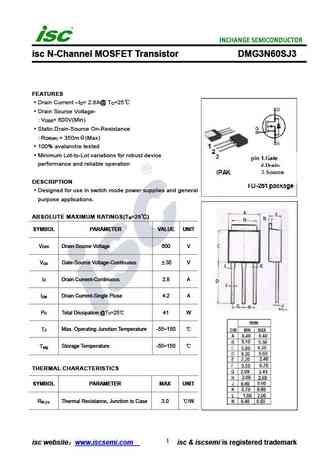
isc N-Channel MOSFET Transistor DMG3N60SJ3 FEATURES Drain Current I = 2.8A@ T =25 D C Drain Source Voltage- V = 600V(Min) DSS Static Drain-Source On-Resistance R = 350m (Max) DS(on) 100% avalanche tested Minimum Lot-to-Lot variations for robust device performance and reliable operation DESCRIPTION Designed for use in switch mode power supplies and general p
Otros transistores... UK2996, 1N60A, 1N60, 1N60P, 1N60Z, 2N60L, 2N60, 2N60K, 50N06, 3N60A, 3N60Z, 3N60K, 4N60, 4N60Z, 4N60K, 8N50H, 9N50
Parámetros del MOSFET. Cómo se afectan entre sí.
🌐 : EN ES РУ

Liste
Recientemente añadidas las descripciónes de los transistores:
MOSFET: CEZC2P07 | CEZ2R05 | CEU3133 | CES2361 | CES2312A | CEP100N10L | CEM3425 | CEM3139 | CEM3133 | CEM3115 | CED3133 | CEC3257 | CEC2533 | CEB100N10L | BC3134KT | BC3134K
Popular searches
2sc1815 equivalent | 2sa1220 | 2sa940 | 2sc627 | 2sc680 | 2sd234 | 2sc9014 | a970 transistor