24N50 MOSFET Equivalente. Reemplazo. Hoja de especificaciones. Principales características
Número de Parte: 24N50
Tipo de FET: MOSFET
Polaridad de transistor: N
ESPECIFICACIONES MÁXIMAS
Pdⓘ - Máxima disipación de potencia: 290
W
|Vds|ⓘ - Voltaje máximo drenador - fuente: 500
V
|Vgs|ⓘ - Voltaje máximo fuente - puerta: 30
V
|Id|ⓘ - Corriente continua de drenaje: 24
A
Tjⓘ - Temperatura máxima de unión: 150
°C
CARACTERÍSTICAS ELÉCTRICAS
trⓘ - Tiempo de subida: 250
nS
Cossⓘ - Capacitancia
de salida: 520
pF
Rds(on)ⓘ - Resistencia estado encendido drenaje a fuente: 0.15
Ohm
Paquete / Cubierta:
TO-247
TO-3P
Búsqueda de reemplazo de 24N50 MOSFET
-
Selección ⓘ de transistores por parámetros
24N50 datasheet
..1. Size:210K utc
24n50.pdf 
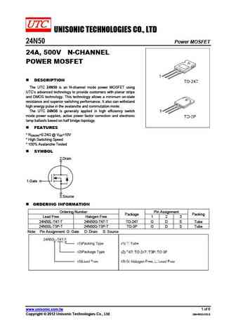
UNISONIC TECHNOLOGIES CO., LTD 24N50 Power MOSFET 24A, 500V N-CHANNEL POWER MOSFET DESCRIPTION The UTC 24N50 is an N-channel mode power MOSFET using UTC s advanced technology to provide customers with planar stripe and DMOS technology. This technology allows a minimum on-state resistance and superior switching performance. It also can withstand high energy pulse in the aval
0.1. Size:1520K fairchild semi
fqa24n50.pdf
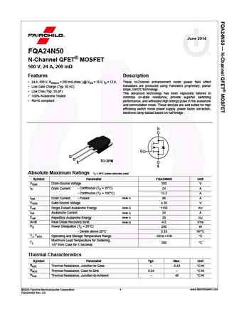
June 2014 FQA24N50 N-Channel QFET MOSFET 500 V, 24 A, 200 m Features Description 24 A, 500 V, RDS(on) = 200 m (Max.) @ VGS = 10 V, ID = 12 A These N-Channel enhancement mode power field effect transistors are produced using Fairchild s proprietary, planar Low Gate Charge (Typ. 90 nC) stripe, DMOS technology. Low Crss (Typ. 55 pF) This advanced technology has been e
0.2. Size:688K fairchild semi
fda24n50.pdf
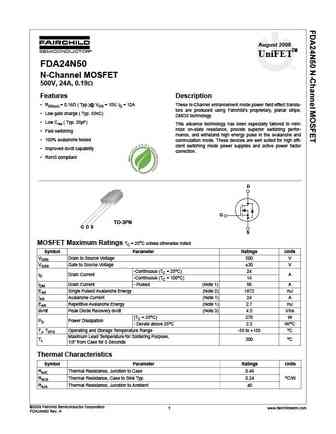
August 2008 UniFETTM FDA24N50 N-Channel MOSFET 500V, 24A, 0.19 Features Description RDS(on) = 0.16 ( Typ.)@ VGS = 10V, ID = 12A These N-Channel enhancement mode power field effect transis- tors are produced using Fairchild s proprietary, planar stripe, Low gate charge ( Typ. 65nC) DMOS technology. Low Crss ( Typ. 35pF) This advance technology has been especially t
0.3. Size:749K fairchild semi
fqa24n50 f109.pdf
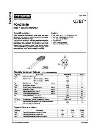
April 2000 TM QFET QFET QFET QFET 500V N-ChanneI MOSFET GeneraI Description Features These N-Channel enhancement mode power field effect 24A, 500V, RDS(on) = 0.2 @VGS = 10 V transistors are produced using Fairchild s proprietary, Low gate charge ( typical 90 nC) planar stripe, DMOS technology. Low Crss ( typical 55 pF) This advanced technology has been e
0.4. Size:641K fairchild semi
fqa24n50f.pdf
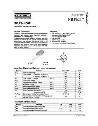
September 2001 TM FRFET FQA24N50F 500V N-Channel MOSFET General Description Features These N-Channel enhancement mode power field effect 24A, 500V, RDS(on) = 0.2 @VGS = 10 V transistors are produced using Fairchild s proprietary, Low gate charge ( typical 90 nC) planar stripe, DMOS technology. Low Crss ( typical 55 pF) This advanced technology has been especially tail
0.5. Size:670K fairchild semi
fda24n50f.pdf
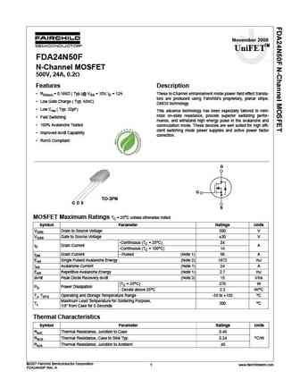
November 2008 UniFETTM FDA24N50F tm N-Channel MOSFET 500V, 24A, 0.2 Features Description RDS(on) = 0.166 ( Typ.)@ VGS = 10V, ID = 12A These N-Channel enhancement mode power field effect transis- tors are produced using Fairchild s proprietary, planar stripe, Low Gate Charge ( Typ. 65nC) DMOS technology. Low Crss ( Typ. 32pF) This advance technology has been esp
0.8. Size:145K ixys
ixfh24n50q ixft24n50q ixfh26n50q ixft26n50q.pdf
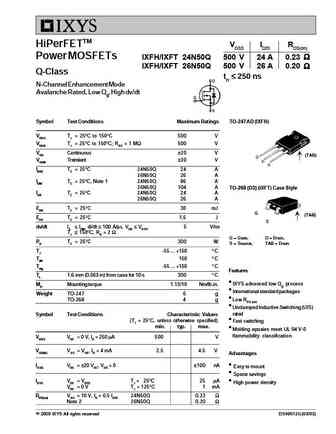
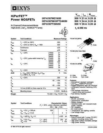
HiPerFETTM VDSS ID25 RDS(on) Power MOSFETs IXFH/IXFT 24N50Q 500 V 24 A 0.23 IXFH/IXFT 26N50Q 500 V 26 A 0.20 Q-Class trr 250 ns N-Channel Enhancement Mode Avalanche Rated, Low Qg, High dv/dt Symbol Test Conditions Maximum Ratings TO-247 AD (IXFH) VDSS TJ = 25 C to 150 C 500 V VDGR TJ = 25 C to 150 C; RGS = 1
0.9. Size:133K ixys
ixgh24n50bu1 ixgh24n60bu1.pdf
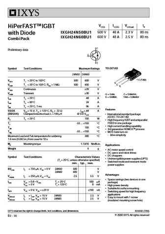
VCES IC(25) VCE(sat) tfi HiPerFASTTM IGBT 500 V 48 A 2.3 V 80 ns IXGH24N50BU1 with Diode 600 V 48 A 2.5 V 80 ns IXGH24N60BU1 Combi Pack Preliminary data TO-247 AD Symbol Test Conditions Maximum Ratings 24N50 24N60 C (TAB) VCES TJ = 25 C to 150 C 500 600 V G VCGR TJ = 25 C to 150 C; RGE = 1 M 500 600 V C E VGES Continuous 20 V VGEM Transient 30 V G = Gate, C = Collector, E
0.10. Size:33K ixys
ixfr24n50 ixfr26n50.pdf
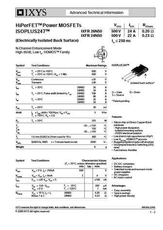
Advanced Technical Information VDSS ID25 RDS(on) HiPerFETTM Power MOSFETs IXFR 26N50 500 V 24 A 0.20 W ISOPLUS247TM IXFR 24N50 500 V 22 A 0.23 W (Electrically Isolated Back Surface) trr 250 ns N-Channel Enhancement Mode High dV/dt, Low trr, HDMOSTM Family ISOPLUS 247TM Symbol Test Conditions Maximum Ratings VDSS TJ = 25 C to 150 C 500 V VDGR TJ = 25 C to 150 C; RGS = 1 MW 50
0.11. Size:78K ixys
ixfr24n50q ixfr26n50q.pdf
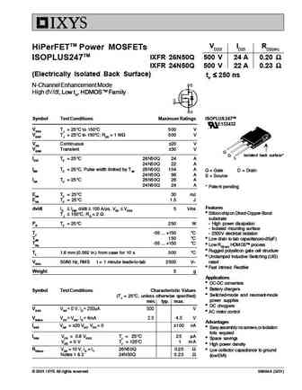
VDSS ID25 RDS(on) HiPerFETTM Power MOSFETs IXFR 26N50Q 500 V 24 A 0.20 ISOPLUS247TM IXFR 24N50Q 500 V 22 A 0.23 (Electrically Isolated Back Surface) trr 250 ns N-Channel Enhancement Mode High dV/dt, Low t , HDMOSTM Family rr Symbol Test Conditions Maximum Ratings ISOPLUS 247TM E153432 VDSS TJ = 25 C to 150 C
0.12. Size:118K ixys
ixgh24n50b ixgh24n60b.pdf
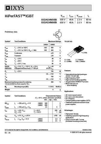
VCES IC(25) VCE(sat) tfi HiPerFASTTM IGBT IXGH24N50B 500 V 48 A 2.3 V 80 ns 600 V 48 A 2.5 V 80 ns IXGH24N60B Preliminary data Symbol Test Conditions Maximum Ratings TO-247 AD 24N50 24N60 VCES TJ = 25 C to 150 C 500 600 V VCGR TJ = 25 C to 150 C; RGE = 1 M 500 600 V C (TAB) VGES Continuous 20 V G VGEM Transient 30 V C E IC25 TC = 25 C48 A G = Gate, C = Collector, IC90 TC = 9
0.13. Size:108K ixys
ixth21n50 ixth24n50 ixtm21n50 ixtm24n50.pdf
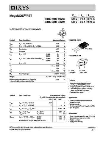
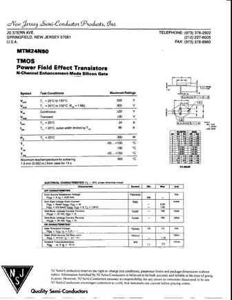
VDSS ID25 RDS(on) MegaMOSTMFET IXTH / IXTM 21N50 500 V 21 A 0.25 IXTH / IXTM 24N50 500 V 24 A 0.23 N-Channel Enhancement Mode Symbol Test Conditions Maximum Ratings TO-247 AD (IXTH) VDSS TJ = 25 C to 150 C 500 V VDGR TJ = 25 C to 150 C; RGS = 1 M 500 V D (TAB) VGS Continuous 20 V VGSM Transient 30 V ID25 TC = 25 C 21N50 21 A
0.14. Size:1524K onsemi
fda24n50f.pdf

Is Now Part of To learn more about ON Semiconductor, please visit our website at www.onsemi.com Please note As part of the Fairchild Semiconductor integration, some of the Fairchild orderable part numbers will need to change in order to meet ON Semiconductor s system requirements. Since the ON Semiconductor product management systems do not have the ability to manage part nomenclatur
0.15. Size:34K microsemi
24n50a.pdf
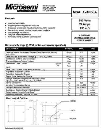
2830 S. Fairview St. Santa Ana, CA 92704 PH (714) 979-8220 FAX (714) 966-5256 MSAFX24N50A Features 500 Volts Ultrafast body diode 24 Amps Rugged polysilicon gate cell structure Increased Unclamped Inductive Switching (UIS) capability 230 m Hermetically sealed, surface mount power package Low package inductance Very low thermal resistance N-CHANNE
0.17. Size:28K ssdi
sff24n50.pdf
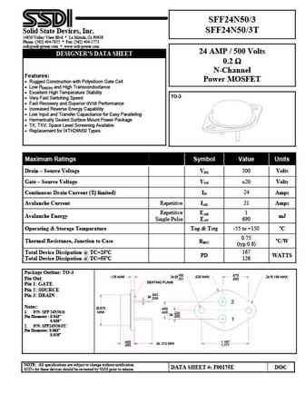
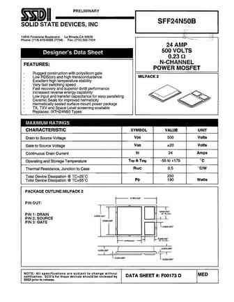
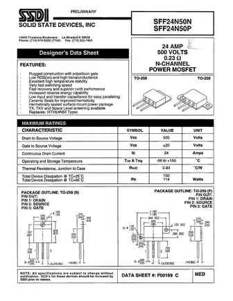
SFF24N50/3 SFF24N50/3T Solid State Devices, Inc. 14830 Valley View Blvd * La Mirada, Ca 90638 Phone (562) 404-7855 * Fax (562) 404-1773 ssdi@ssdi-power.com * www.ssdi-power.com 24 AMP / 500 Volts DESIGNER S DATA SHEET 0.2 N-Channel Features Power MOSFET Rugged Construction with Polysilicon Gate Cell Low R and High Transconductance DS(ON) Excellent H
0.20. Size:990K jilin sino
jcs24n50wh jcs24n50abh.pdf
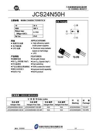
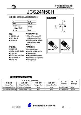
N N- CHANNEL MOSFET R JCS24N50H MAIN CHARACTERISTICS Package ID 24 A VDSS 500 V Rdson-max 0.19 @Vgs=10V Qg-typ 81nC APPLICATIONS High efficiency switch mode power supplies Electronic lamp ballasts UPS based on half bridge
0.22. Size:1209K blue-rocket-elect
bru24n50.pdf
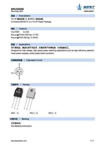
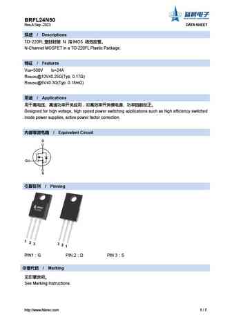
BRU24N50 Rev.A Aug.-2023 DATA SHEET / Descriptions TO-3P N MOS N-Channel MOSFET in a TO-3P Plastic Package. / Features V =500V I =24A DS D R DS(ON)@10V 0.25 (Typ. 0.17 ) R DS(ON)@6V 0.3 (Typ. 0.18m ) / Applications
0.24. Size:484K nell
24n50b 24n50c.pdf
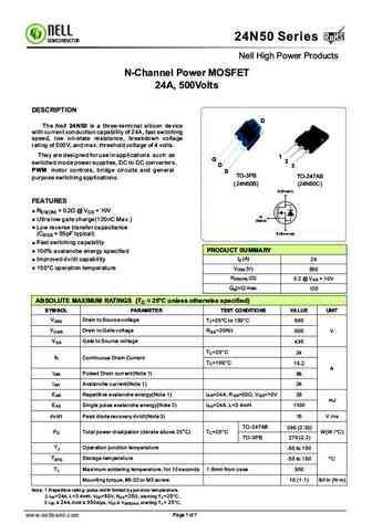
RoHS 24N50 Series RoHS SEMICONDUCTOR Nell High Power Products N-Channel Power MOSFET 24A, 500Volts DESCRIPTION D The Nell 24N50 is a three-terminal silicon device with current conduction capability of 24A, fast switching speed, low on-state resistance, breakdown voltage rating of 500V, and max. threshold voltage of 4 volts. They are designed for use in applications such as G
0.25. Size:678K crhj
cs24n50 anhd.pdf
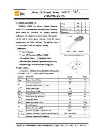
Silicon N-Channel Power MOSFET R CS24N50 ANHD General Description VDSS 500 V CS24N50 ANHD, the silicon N-channel Enhanced ID 24 A PD(TC=25 ) 230 W VDMOSFETs, is obtained by the self-aligned planar Technology RDS(ON)Typ 0.18 which reduce the conduction loss, improve switching performance and enhance the avalanche energy. The transistor can be used in various
0.26. Size:124K china
cs24n50.pdf
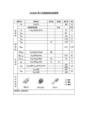
CS24N50 N PD TC=25 300 W 0.40 W/ ID VGS=10V,TC=25 24 A IDM 96 VGS 20 V Tjm +150 Tstg -55 +150 RthJC 0.42 /W BVDSS VGS=0V,ID=0.25mA 500 V RDS on VGS=10V,ID=12A 0.23 VGS th VDS=VGS,ID=4mA 2.
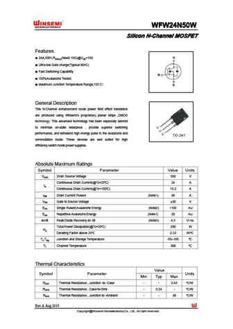
0.27. Size:428K winsemi
wfw24n50n.pdf
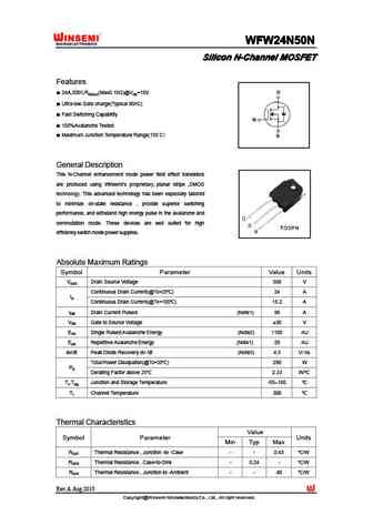
WFW24N50N WFW24N50N WFW24N50N WFW24N50N Silicon N-Channel MOSFET Silicon N-Channel MOSFET Silicon N-Channel MOSFET Silicon N-Channel MOSFET Features 24A,500V,RDS(on)(Max0.19 )@VGS=10V Ultra-low Gate charge(Typical 90nC) Fast Switching Capability 100%Avalanche Tested Maximum Junction Temperature Range(150 ) General Description This N-Channel enhancement mod
0.28. Size:463K winsemi
wfw24n50w.pdf
WFW24N50W WFW24N50W WFW24N50W WFW24N50W Silicon N-Channel MOSFET Silicon N-Channel MOSFET Silicon N-Channel MOSFET Silicon N-Channel MOSFET Features 24A,500V,RDS(on)(Max0.19 )@VGS=10V Ultra-low Gate charge(Typical 90nC) Fast Switching Capability 100%Avalanche Tested Maximum Junction Temperature Range(150 ) General Description This N-Channel enhancement mod
0.30. Size:497K jiaensemi
jfam24n50c.pdf
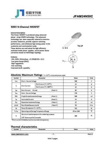
JFAM24N50C 500V N-Channel MOSFET General Description This Power MOSFET is produced using advanced planar stripe DMOS technology. This advanced technology has been especially tailored to minimize on-state resistance, provide superior switching performance, and withstand high energy pulse in the avalanche and commutation mode. These devices are well suited for high efficiency
0.31. Size:505K jiaensemi
jfpc24n50c jffm24n50c.pdf
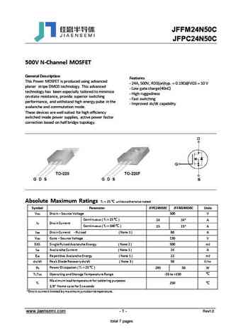
JFFM24N50C JFPC24N50C 500V N-Channel MOSFET General Description Features This Power MOSFET is produced using advanced - 24A, 500V, RDS(on)typ. = 0.19 @VGS = 10 V planar stripe DMOS technology. This advanced - Low gate charge(40nC) technology has been especially tailored to minimize - High ruggedness on-state resistance, provide superior switching - Fast switching perf
0.32. Size:332K kia
kia24n50h.pdf
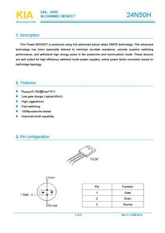
24A 500V 24N50H N-CHANNELMOSFET KIA KIA KIA SEMICONDUCTORS SEMICONDUCTORS SEMICONDUCTORS 1.Description This Power MOSFET is produced using KIAadvanced planar stripe DMOS technology. This advanced technology has been especially tailored to minimize on-state resistance, provide superior switching performance, and withstand high energy pulse in the avalanche and commutation mode. The
0.33. Size:959K maple semi
slw24n50c.pdf
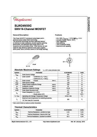
SLW24N50C 500V N-Channel MOSFET General Description Features This Power MOSFET is produced using Maple semi s - 25A, 500V, RDS(on)typ. = 167m @VGS = 10 V advanced planar stripe DMOS technology. - Low gate charge ( typical 96nC) This advanced technology has been especially tailored - High ruggedness to minimize on-state resistance, provide superior switching - Fast switching performanc
0.34. Size:1261K maple semi
slw24n50c slh24n50c.pdf
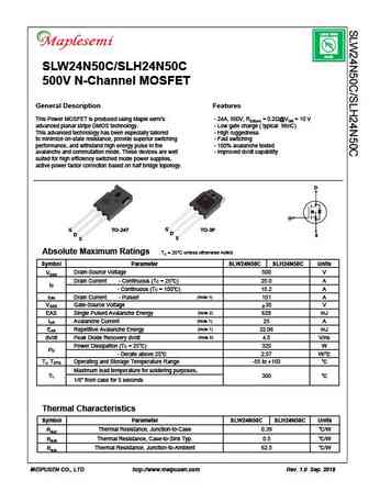
LEAD FREE Pb RoHS SLW24N50C/SLH24N50C 500V N-Channel MOSFET General Description Features This Power MOSFET is produced using Maple semi s - 24A, 500V, RDS(on) = 0.2 @VGS = 10 V advanced planar stripe DMOS technology. - Low gate charge ( typical 96nC) This advanced technology has been especially tailored - High ruggedness to minimize on-state resistance, provide superior switching -
0.35. Size:681K samwin
swt24n50d.pdf
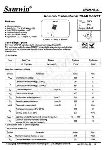
SW24N50D N-channel Enhanced mode TO-247 MOSFET TO-247 BVDSS 500V Features ID 24A High ruggedness RDS(ON) 0.14 Low RDS(ON) (Typ 0.14 )@VGS=10V Low Gate Charge (Typ 129nC) 2 Improved dv/dt Capability 1 100% Avalanche Tested 2 1 3 Application LED , Charger, PC Power 1. Gate 2. Drain 3. Source 3 General Description This p
0.36. Size:184K semihow
hfa24n50g.pdf
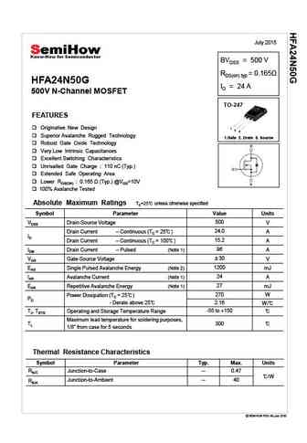
July 2015 BVDSS = 500 V RDS(on) typ HFA24N50G ID = 24 A 500V N-Channel MOSFET TO-247 FEATURES Originative New Design 1 2 3 Superior Avalanche Rugged Technology 1.Gate 2. Drain 3. Source Robust Gate Oxide Technology Very Low Intrinsic Capacitances Excellent Switching Characteristics Unrivalled Gate Charge 110 nC (Typ.) Extended Safe Operating Area Lo
0.37. Size:757K truesemi
tsa24n50m.pdf
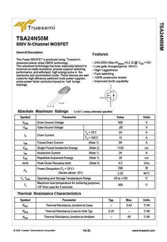
TSA24N50M 500V N-Channel MOSFET General Description Features This Power MOSFET is produced using Truesemi s 24A,500V,Max.RDS(on)=0.2 @ VGS =10V advanced planar stripe DMOS technology. This advanced technology has been especially tailored to Low gate charge(typical 90nC) minimize on-state resistance, provide superior switching High ruggedness performance, and
0.38. Size:4754K first semi
fir24n50aptg.pdf
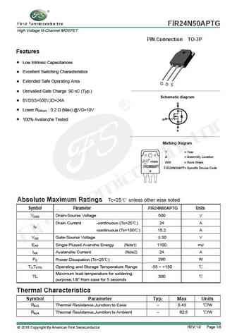
FIR24N50APTG High Voltage N-Channel MOSFET PIN Connection TO-3P Features Low Intrinsic Capacitances Excellent Switching Characteristics Extended Safe Operating Area Unrivalled Gate Charge 90 nC (Typ.) g Schematic dia ram BVDSS=500V,ID=24A D Lower RDS(on) 0.2 (Max) @VG=10V G 100% Avalanche Tested S Marking Diagram Y = Year A = Assembly Location
0.39. Size:1014K cn sinai power
spa24n50g.pdf
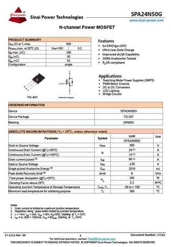
SPA24N50G Sinai Power Technologies www.sinai-power.com N-channel Power MOSFET PRODUCT SUMMARY Features V (V) at T max. 500 DS J ID=24A(Vgs=10V) R max. at 25oC ( ) V =10V 0.2 DS(on) GS Ultra Low Gate Charge Q max. (nC) 160 g Improved dv/dt Capability Q (nC) 30 gs 100% Avalanche Tested Q (nC) 53 gd ROHS compliant Configuration single A
0.40. Size:2593K cn hmsemi
hm24n50a.pdf
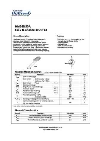
HM24N50A 500V N-Channel MOSFET General Description Features This Power MOSFET is produced using Maple semi s - 25A, 500V, RDS(on)typ. = 167m @VGS = 10 V advanced planar stripe DMOS technology. - Low gate charge ( typical 96nC) This advanced technology has been especially tailored - High ruggedness to minimize on-state resistance, provide superior switching - Fast switching performance
0.41. Size:253K inchange semiconductor
ixtm24n50.pdf
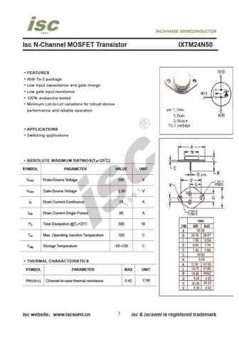
Isc N-Channel MOSFET Transistor IXTM24N50 FEATURES With To-3 package Low input capacitance and gate charge Low gate input resistance 100% avalanche tested Minimum Lot-to-Lot variations for robust device performance and reliable operation APPLICATIONS Switching applications ABSOLUTE MAXIMUM RATINGS(T =25 ) a SYMBOL PARAMETER VALUE UNIT V Drain-Source Voltage 500
0.42. Size:210K inchange semiconductor
fqa24n50f.pdf
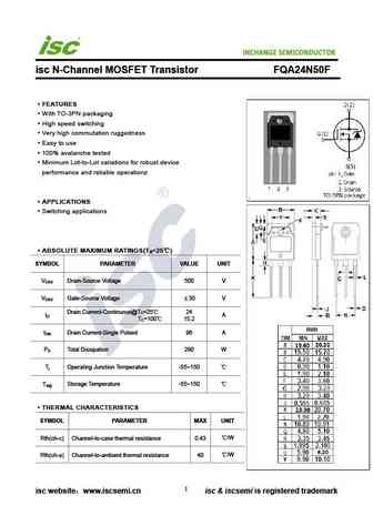
INCHANGE Semiconductor isc N-Channel MOSFET Transistor FQA24N50F FEATURES With TO-3PN packaging High speed switching Very high commutation ruggedness Easy to use 100% avalanche tested Minimum Lot-to-Lot variations for robust device performance and reliable operationz APPLICATIONS Switching applications ABSOLUTE MAXIMUM RATINGS(T =25 ) a SYMBOL PARAMETER VALUE
0.43. Size:209K inchange semiconductor
fda24n50f.pdf
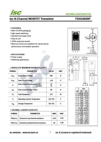
INCHANGE Semiconductor isc N-Channel MOSFET Transistor FDA24N50F FEATURES With TO-3PN packaging High speed switching Standard level gate drive Easy to use 100% avalanche tested Minimum Lot-to-Lot variations for robust device performance and reliable operation APPLICATIONS Power supply Switching applications ABSOLUTE MAXIMUM RATINGS(T =25 ) a SYMBOL PARAMET
Otros transistores... 10N50
, 11N50
, 12N50
, 13N50
, 14N50
, 15N50
, 16N50
, 18N50
, 7N65
, 26N50
, UF830
, UF830Z
, UF840
, UK3568
, UF450
, UF460
, 1N50
.