9N40 Datasheet. Equivalente. Reemplazo. Hoja de especificaciones. Principales características
Número de Parte: 9N40 📄📄
Tipo de FET: MOSFET
Polaridad de transistor: N
ESPECIFICACIONES MÁXIMAS
Pdⓘ - Máxima disipación de potencia: 113 W
|Vds|ⓘ - Voltaje máximo drenador-fuente: 400 V
|Vgs|ⓘ - Voltaje máximo fuente-puerta: 30 V
|Id|ⓘ - Corriente continua de drenaje: 9 A
Tjⓘ - Temperatura máxima de unión: 150 °C
CARACTERÍSTICAS ELÉCTRICAS
trⓘ - Tiempo de subida: 60 nS
Cossⓘ - Capacitancia de salida: 160 pF
RDSonⓘ - Resistencia estado encendido drenaje a fuente: 0.6 Ohm
Encapsulados: TO-220
TO-220F1
📄📄 Copiar
Búsqueda de reemplazo de 9N40 MOSFET
- Selecciónⓘ de transistores por parámetros
9N40 datasheet
..1. Size:153K utc
9n40.pdf 
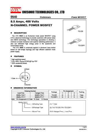
UNISONIC TECHNOLOGIES CO., LTD 9N40 Preliminary Power MOSFET 8.5 Amps, 400 Volts N-CHANNEL POWER MOSFET 1 TO-220 DESCRIPTION The UTC 9N40 is an N-channel mode power MOSFET using UTC s advanced technology to provide customers with planar stripe and DMOS technology. This technology specializes in allowing a minimum on-state resistance and superior switching performance. It 1
..2. Size:2008K goford
9n40.pdf
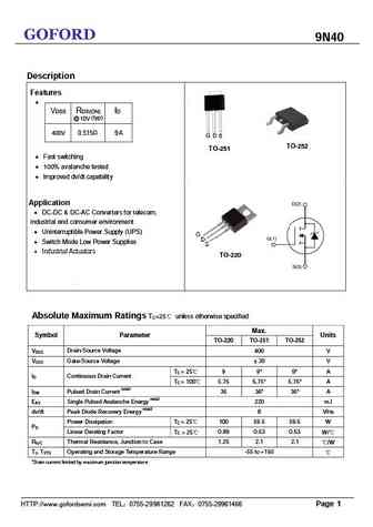
GOFORD 9N40 Description Features VDSS RDS(ON) ID @ 10V (typ) 0.515 9A 400V TO-252 TO-251 Fast switching 100% avalanche tested Improved dv/dt capability Application DC-DC & DC-AC Converters for telecom, industrial and consumer environment Uninterruptible Power Supply (UPS) Switch Mode Low Power Supplies Industrial Actuators T
..3. Size:227K inchange semiconductor
9n40.pdf
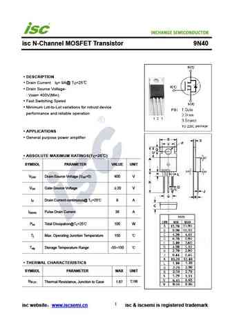
INCHANGE Semiconductor isc N-Channel MOSFET Transistor 9N40 DESCRIPTION Drain Current I = 9A@ T =25 D C Drain Source Voltage- V = 400V(Min) DSS Fast Switching Speed Minimum Lot-to-Lot variations for robust device performance and reliable operation APPLICATIONS General purpose power amplifier ABSOLUTE MAXIMUM RATINGS(T =25 ) C SYMBOL PARAMETER VALUE UNIT V
0.1. Size:601K st
stgd19n40lz.pdf
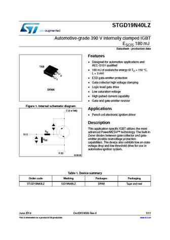
STGD19N40LZ Automotive-grade 390 V internally clamped IGBT ESCIS 180 mJ Datasheet - production data Features Designed for automotive applications and AEC-Q101 qualified TAB 180 mJ of avalanche energy @ TC = 150 C, L = 3 mH 3 ESD gate-emitter protection 1 Gate-collector high voltage clamping Logic level gate drive DPAK Low saturation voltage Hig
0.2. Size:841K st
std9n40m2.pdf
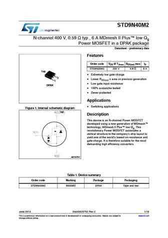
STD9N40M2 N-channel 400 V, 0.59 typ., 6 A MDmesh II Plus low Qg Power MOSFET in a DPAK package Datasheet - preliminary data Features Order code VDS @ TJmax RDS(on) max ID STD9N40M2 450 V 0.8 6 A TAB Extremely low gate charge 3 Lower RDS(on) x area vs previous generation 1 Low gate input resistance DPAK 100% avalanche tested Zener-protected Applica
0.3. Size:258K fairchild semi
fdp19n40 fdpf19n40.pdf
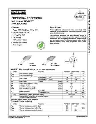
October UniFETTM FDP19N40 / FDPF19N40 tm N-Channel MOSFET 400V, 19A, 0.24 Features Description RDS(on) =0.2 ( Typ.)@ VGS = 10V, ID = 9.5A These N-Channel enhancement mode power field effect transistors are produced using Fairchild s proprietary, planar Low Gate Charge ( Typ. 32nC) stripe, DMOS technology. Low Crss ( Typ. 20pF) This advanced technology has been
0.4. Size:681K onsemi
fdp19n40.pdf

Is Now Part of To learn more about ON Semiconductor, please visit our website at www.onsemi.com Please note As part of the Fairchild Semiconductor integration, some of the Fairchild orderable part numbers will need to change in order to meet ON Semiconductor s system requirements. Since the ON Semiconductor product management systems do not have the ability to manage part nomenclatur
0.5. Size:906K kec
kf9n40d.pdf
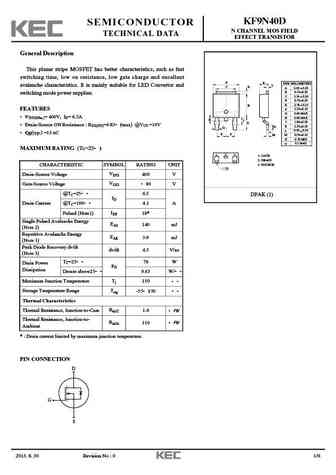
KF9N40D SEMICONDUCTOR N CHANNEL MOS FIELD TECHNICAL DATA EFFECT TRANSISTOR General Description This planar stripe MOSFET has better characteristics, such as fast switching time, low on resistance, low gate charge and excellent A K DIM MILLIMETERS avalanche characteristics. It is mainly suitable for LED Convertor and L C D _ A 6.60 + 0.20 _ B 6.10 + 0.20 switching mode power sup
0.6. Size:522K kec
kmb3d9n40ta.pdf
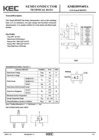
SEMICONDUCTOR KMB3D9N40TA TECHNICAL DATA N-Ch Trench MOSFET General Description This Trench MOSFET has better characteristics, such as fast switching time, low on resistance, low gate charge and excellent avalanche E characteristics. It is mainly suitable for Load switch and Back-Light B K DIM MILLIMETERS Inverter. _ A 2.9 + 0.2 B 1.6+0.2/-0.1 _ C 0.70 + 0.05 2 3 _ D 0.4 + 0
0.7. Size:252K aosemi
aot9n40.pdf
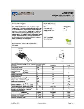
AOT9N40 400V,8A N-Channel MOSFET General Description Product Summary VDS The AOT9N40 is fabricated using an advanced high 500V@150 voltage MOSFET process that is designed to deliver high ID (at VGS=10V) 8A levels of performance and robustness in popular AC-DC
0.8. Size:261K aosemi
aod9n40.pdf
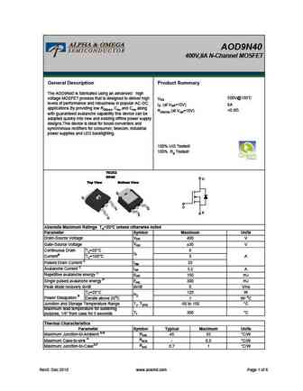
AOD9N40 400V,8A N-Channel MOSFET General Description Product Summary The AOD9N40 is fabricated using an advanced high voltage MOSFET process that is designed to deliver high 500V@150 VDS levels of performance and robustness in popular AC-DC ID (at VGS=10V) 8A applications.By providing low RDS(on), Ciss and Crss along
0.9. Size:252K aosemi
aot9n40l.pdf

AOT9N40 400V,8A N-Channel MOSFET General Description Product Summary VDS The AOT9N40 is fabricated using an advanced high 500V@150 voltage MOSFET process that is designed to deliver high ID (at VGS=10V) 8A levels of performance and robustness in popular AC-DC
0.10. Size:426K crhj
cs19n40 a8h.pdf
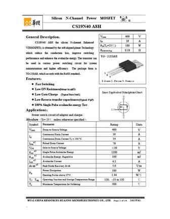
Silicon N-Channel Power MOSFET R CS19N40 A8H VDSS 400 V General Description ID 19 A CS19N40 A8H the silicon N-channel Enhanced PD(TC=25 ) 180 W VDMOSFETs, is obtained by the self-aligned planar Technology RDS(ON)Typ 0.18 which reduce the conduction loss, improve switching performance and enhance the avalanche energy. The transistor can be used in various pow
0.11. Size:438K crhj
cs19n40 an.pdf
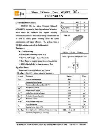
Silicon N-Channel Power MOSFET R CS19N40 AN VDSS 400 V General Description ID 19 A CS19N40 AN, the silicon N-channel Enhanced PD(TC=25 ) 180 W VDMOSFETs, is obtained by the self-aligned planar Technology RDS(ON)Typ 0.18 which reduce the conduction loss, improve switching performance and enhance the avalanche energy. The transistor can be used in various power
0.12. Size:834K magnachip
mdd9n40rh.pdf
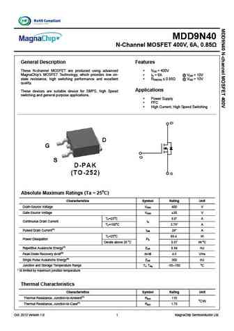
MDD9N40 N-Channel MOSFET 400V, 6A, 0.85 General Description Features These N-channel MOSFET are produced using advanced VDS = 400V MagnaChip s MOSFET Technology, which provides low on- ID = 6A @ VGS = 10V state resistance, high switching performance and excellent RDS(ON) 0.85 @ VGS = 10V quality. Applications These devices are suitable device for SMPS, high Speed s
0.13. Size:1048K belling
bl19n40-p bl19n40-a.pdf
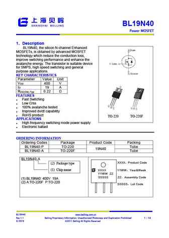
BL19N40 Power MOSFET 1 Description Step-Down Converter BL19N40, the silicon N-channel Enhanced , MOSFETs, is obtained by advanced MOSFET technology which reduce the conduction loss, improve switching performance and enhance the avalanche energy. The transistor is suitable device for SMPS, high speed switching and general purpose applications. KEY CHARACTERISTICS Par
0.14. Size:426K wuxi china
cs19n40a8h.pdf

Silicon N-Channel Power MOSFET R CS19N40 A8H VDSS 400 V General Description ID 19 A CS19N40 A8H the silicon N-channel Enhanced PD(TC=25 ) 180 W VDMOSFETs, is obtained by the self-aligned planar Technology RDS(ON)Typ 0.18 which reduce the conduction loss, improve switching performance and enhance the avalanche energy. The transistor can be used in various pow
0.15. Size:438K wuxi china
cs19n40an.pdf

Silicon N-Channel Power MOSFET R CS19N40 AN VDSS 400 V General Description ID 19 A CS19N40 AN, the silicon N-channel Enhanced PD(TC=25 ) 180 W VDMOSFETs, is obtained by the self-aligned planar Technology RDS(ON)Typ 0.18 which reduce the conduction loss, improve switching performance and enhance the avalanche energy. The transistor can be used in various power
0.16. Size:439K cn hmsemi
hm19n40.pdf
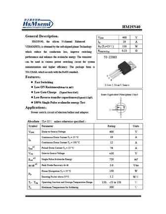
General Description VDSS 400 V HM19N40, the silicon N-channel Enhanced ID 19 A PD (TC=25 ) 150 W VDMOSFETs, is obtained by the self-aligned planar Technology RDS(ON)Typ 0.23 which reduce the conduction loss, improve switching performance and enhance the avalanche energy. The transistor can be used in various power switching circuit for system miniaturizatio
0.17. Size:796K cn fx-semi
fxn9n40c.pdf
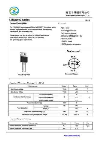
FuXin Semiconductor Co., Ltd. FXN9N40C Series Rev.A General Description Features The FXN9N40C uses advanced Silicon s MOSFET Technology, which VDS = 400V provides high performance in on-state resistance, fast switching ID = 10A @VGS = 10V performance, and excellent quality. Very low on-resistance These devices can also be utilized in industria
0.18. Size:261K inchange semiconductor
aot9n40.pdf
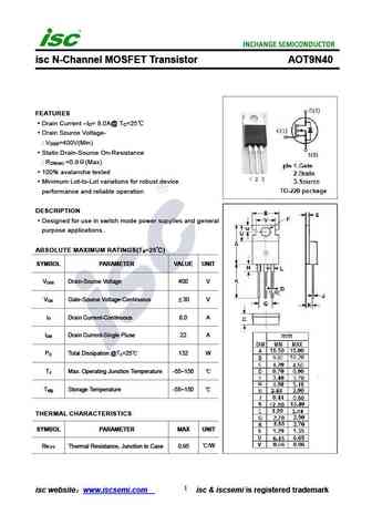
isc N-Channel MOSFET Transistor AOT9N40 FEATURES Drain Current I = 8.0A@ T =25 D C Drain Source Voltage- V =400V(Min) DSS Static Drain-Source On-Resistance R =0.8 (Max) DS(on) 100% avalanche tested Minimum Lot-to-Lot variations for robust device performance and reliable operation DESCRIPTION Designed for use in switch mode power supplies and general purpose
0.19. Size:262K inchange semiconductor
fdp19n40.pdf
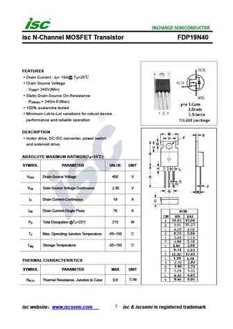
isc N-Channel MOSFET Transistor FDP19N40 FEATURES Drain Current I = 19A@ T =25 D C Drain Source Voltage V = 240V(Min) DSS Static Drain-Source On-Resistance R = 240m (Max) DS(on) 100% avalanche tested Minimum Lot-to-Lot variations for robust device performance and reliable operation DESCRIPTION motor drive, DC-DC converter, power switch and solenoid drive. A
0.20. Size:265K inchange semiconductor
aod9n40.pdf
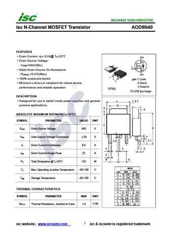
isc N-Channel MOSFET Transistor AOD9N40 FEATURES Drain Current I = 8.0A@ T =25 D C Drain Source Voltage- V =400V(Min) DSS Static Drain-Source On-Resistance R =0.8 (Max) DS(on) 100% avalanche tested Minimum Lot-to-Lot variations for robust device performance and reliable operation DESCRIPTION Designed for use in switch mode power supplies and general purpose
Otros transistores... 1N40, 2N40, 3N40, 4N40, 5N40, 6N40, 7N40, 8N40, CS150N03A8, 10N40, 11N40, 12N40, 13N40, 15N40, 18N40, 20N40, 25N40
