AO3415 MOSFET Equivalente. Reemplazo. Hoja de especificaciones. Principales características
Número de Parte: AO3415
Tipo de FET: MOSFET
Polaridad de transistor: P
ESPECIFICACIONES MÁXIMAS
Pdⓘ - Máxima
disipación de potencia: 1.5 W
|Vds|ⓘ - Voltaje máximo drenador-fuente: 20 V
|Vgs|ⓘ - Voltaje máximo fuente-puerta: 8 V
|Id|ⓘ - Corriente continua
de drenaje: 4 A
Tjⓘ - Temperatura máxima de unión: 150 °C
CARACTERÍSTICAS ELÉCTRICAS
trⓘ - Tiempo
de subida: 9 nS
Cossⓘ - Capacitancia de salida: 115 pF
RDSonⓘ - Resistencia estado encendido drenaje a fuente: 0.041 Ohm
Encapsulados: SOT23
Búsqueda de reemplazo de AO3415 MOSFET
- Selecciónⓘ de transistores por parámetros
AO3415 datasheet
..1. Size:283K aosemi
ao3415.pdf 
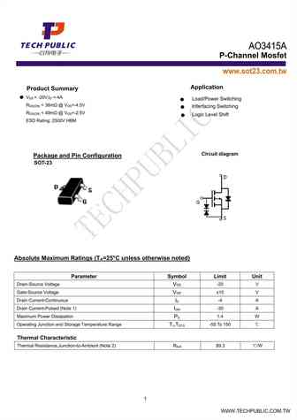
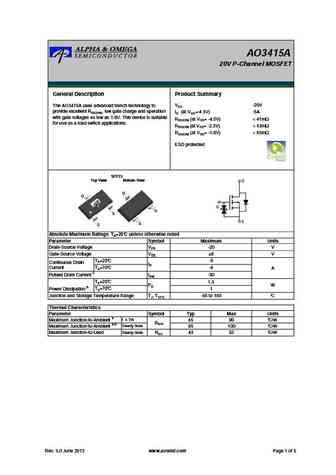
AO3415 20V P-Channel MOSFET General Description Product Summary VDS -20V The AO3415 uses advanced trench technology to provide excellent RDS(ON), low gate charge and operation with gate ID (at VGS=-4.5V) -4A voltages as low as 1.8V. This device is suitable for use as RDS(ON) (at VGS= -4.5V)
..2. Size:1085K shenzhen
ao3415.pdf
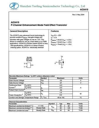
Shenzhen Tuofeng Semiconductor Technology Co., Ltd AO3415 Rev 3 May 2004 AO3415 P-Channel Enhancement Mode Field Effect Transistor General Description Features The AO3415 uses advanced trench technology to VDS (V) = -20V provide excellent RDS(ON), low gate charge and ID = -4 A operation with gate voltages as low as 1.8V. This RDS(ON)
..3. Size:1982K kexin
ao3415.pdf
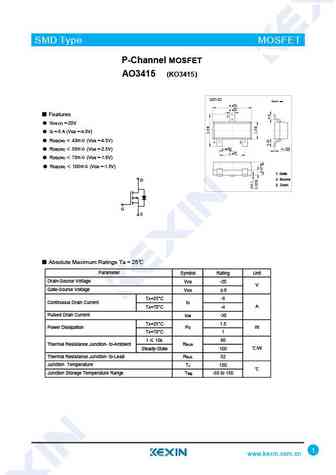
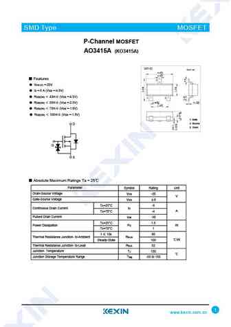
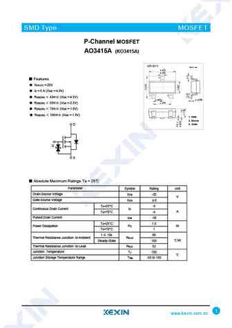
SMD Type MOSFET P-Channel MOSFET AO3415 (KO3415) SOT-23 Unit mm +0.1 2.9-0.1 +0.1 0.4 -0.1 Features 3 VDS (V) =-20V ID =-5 A (VGS =-4.5V) RDS(ON) 43m (VGS =-4.5V) 1 2 +0.1 0.95-0.1 0.1+0.05 RDS(ON) 55m (VGS =-2.5V) -0.01 +0.1 1.9-0.1 RDS(ON) 75m (VGS =-1.8V) RDS(ON) 100m (VGS =-1.5V) 1. Gate 2. Source D 3. Drain
..4. Size:1998K kexin
ao3415 ko3415.pdf
SMD Type MOSFET P-Channel MOSFET AO3415 (KO3415) SOT-23-3 Unit mm +0.2 2.9-0.1 +0.1 0.4 -0.1 Features 3 VDS (V) =-20V ID =-5 A (VGS =-4.5V) RDS(ON) 43m (VGS =-4.5V) 1 2 RDS(ON) 55m (VGS =-2.5V) +0.02 +0.1 0.15 -0.02 0.95 -0.1 +0.1 1.9-0.2 RDS(ON) 75m (VGS =-1.8V) RDS(ON) 100m (VGS =-1.5V) 1. Gate D 2. Source 3
..5. Size:372K guangdong hottech
ao3415.pdf
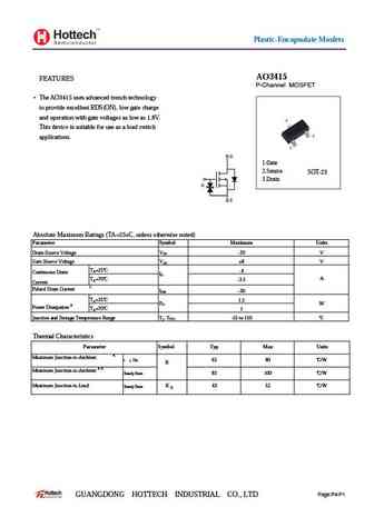
Plastic-Encapsulate Mosfets AO3415 FEATURES P-Channel MOSFET The AO3415 uses advanced trench technology to provide excellent RDS(ON), low gate charge and operation with gate voltages as low as 1.8V. This device is suitable for use as a load switch applications. D 1.Gate 2.Source SOT-23 3.Drain G S Absolute Maximum Ratings (TA=25oC, unless otherwise noted) Parameter Symbol Maxim
..6. Size:1018K huashuo
ao3415.pdf
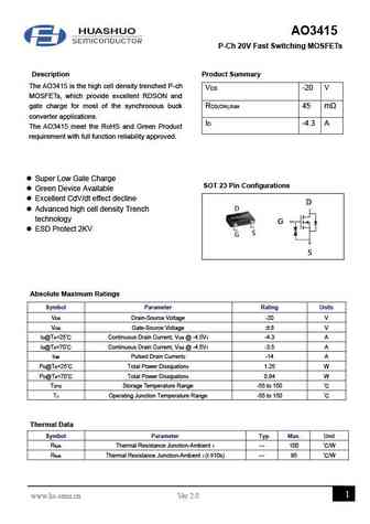
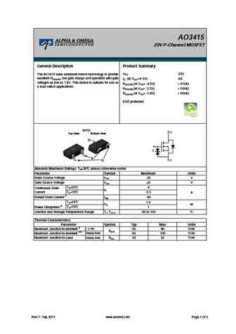
AO3415 P-Ch 20V Fast Switching MOSFETs Description Product Summary The AO3415 is the high cell density trenched P-ch VDS -20 V MOSFETs, which provide excellent RDSON and gate charge for most of the synchronous buck RDS(ON),max 45 m converter applications. ID -4.3 A The AO3415 meet the RoHS and Green Product requirement with full function reliability approved. Super L
..7. Size:1668K mdd
ao3415.pdf
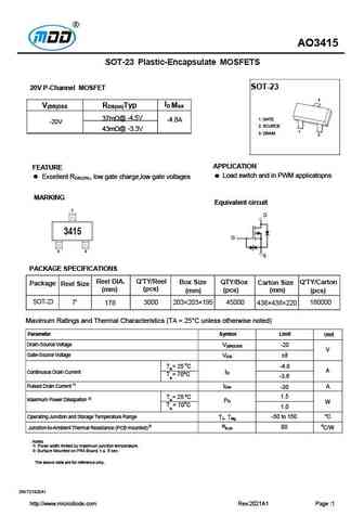
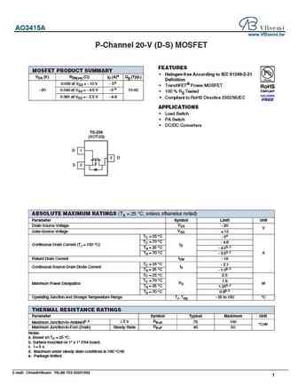
AO3415 SOT-23 Plastic-Encapsulate MOSFETS SOT-23 20V P-Channel MOSFET 3 ID Max V(BR)DSS RDS(on)Typ 37m @ -4.5V 1. GATE -4.8A -20V 2. SOURCE 43m @ -3.3V 1 3. DRAIN 2 APPLICATION FEATURE Load switch and in PWM applicatopns Excellent RDS(ON), low gate charge,low gate voltages MARKING Equivalent circuit D 3415 G S PACKAGE SPECIFICATIONS Reel DI
..8. Size:607K cn puolop
ao3415.pdf
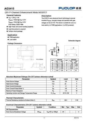
AO3415 -20V P-Channel Enhancement Mode MOSFET General Features Description VDS = -20V,ID =-4A The AO3415 uses advanced trench technology to provide RDS(ON)
..9. Size:1172K cn alj
ao3415.pdf
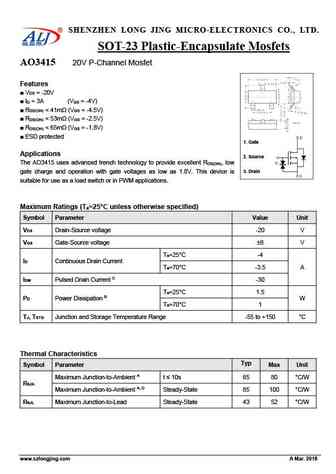
SHENZHEN LONG JING MICRO-ELECTRONICS CO., LTD. SOT-23 Plastic-Encapsulate Mosfets AO3415 20V P-Channel Mosfet Features V = -20V DS I = 3A (V = -4V) D GS R
0.1. Size:319K aosemi
ao3415a.pdf
AO3415A 20V P-Channel MOSFET General Description Product Summary VDS -20V The AO3415A uses advanced trench technology to provide excellent RDS(ON), low gate charge and operation ID (at VGS=-4.5V) -5A with gate voltages as low as 1.8V. This device is suitable RDS(ON) (at VGS= -4.5V)
0.2. Size:378K aosemi
ao3415c.pdf
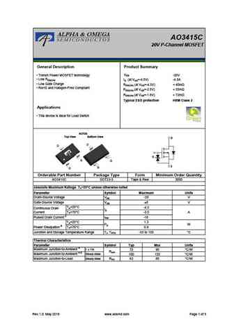
AO3415C 20V P-Channel MOSFET General Description Product Summary VDS Trench Power MOSFET technology -20V Low RDS(ON) ID (at VGS=-4.5V) -4.5A Low Gate Charge RDS(ON) (at VGS=-4.5V)
0.3. Size:1729K kexin
ao3415a.pdf
SMD Type MOSFET P-Channel MOSFET AO3415A (KO3415A) SOT-23 Unit mm +0.1 2.9-0.1 +0.1 0.4 -0.1 Features 3 VDS (V) =-20V ID =-5 A (VGS =-4.5V) RDS(ON) 43m (VGS =-4.5V) 1 2 +0.1 0.95-0.1 0.1+0.05 RDS(ON) 55m (VGS =-2.5V) -0.01 +0.1 1.9-0.1 RDS(ON) 75m (VGS =-1.8V) RDS(ON) 100m (VGS =-1.5V) 1. Gate 2. Source D 3. Dra
0.4. Size:1656K kexin
ao3415w.pdf
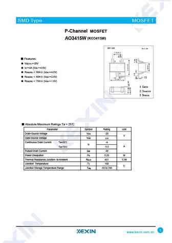
SMD Type MOSFET P-Channel MOSFET (KO3415W) AO3415W Features VDS (V) =-20V ID =-4A (VGS =-4.5V) RDS(ON) 50m (VGS =-4.5V) RDS(ON) 60m (VGS =-2.5V) RDS(ON) 75m (VGS =-1.8V) 1 Gate 2 Source 3 Drain Absolute Maximum Ratings Ta = 25 Parameter Symbol Rating Unit Drain-Source Voltage VDS -20 V Gate-Source Voltage VGS 8 Conti
0.5. Size:1662K kexin
ao3415as.pdf
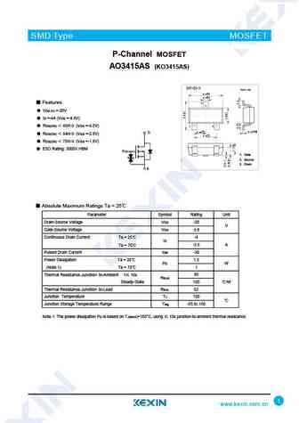
SMD Type MOSFET P-Channel MOSFET AO3415AS (KO3415AS) SOT-23-3 Unit mm +0.2 2.9 -0.1 +0.1 0.4-0.1 Features 3 VDS (V) =-20V ID =-4A (VGS =-4.5V) RDS(ON) 45m (VGS =-4.5V) 1 2 +0.02 +0.1 0.15 -0.02 0.95 -0.1 D RDS(ON) 54m (VGS =-2.5V) +0.1 1.9 -0.2 RDS(ON) 75m (VGS =-1.8V) ESD Rating 3000V HBM G 1. Gate 2. Source 3. Dra
0.6. Size:1998K kexin
ao3415-3.pdf

SMD Type MOSFET P-Channel MOSFET AO3415 (KO3415) SOT-23-3 Unit mm +0.2 2.9-0.1 +0.1 0.4 -0.1 Features 3 VDS (V) =-20V ID =-5 A (VGS =-4.5V) RDS(ON) 43m (VGS =-4.5V) 1 2 RDS(ON) 55m (VGS =-2.5V) +0.02 +0.1 0.15 -0.02 0.95 -0.1 +0.1 1.9-0.2 RDS(ON) 75m (VGS =-1.8V) RDS(ON) 100m (VGS =-1.5V) 1. Gate D 2. Source 3
0.7. Size:1694K kexin
ao3415a-3.pdf
SMD Type MOSFET P-Channel MOSFET AO3415A (KO3415A) SOT-23-3 Unit mm +0.2 2.9 -0.1 +0.1 0.4 -0.1 3 Features VDS (V) =-20V ID =-5 A (VGS =-4.5V) 1 2 RDS(ON) 43m (VGS =-4.5V) +0.02 +0.1 0.15 -0.02 0.95 -0.1 +0.1 1.9 -0.2 RDS(ON) 55m (VGS =-2.5V) RDS(ON) 75m (VGS =-1.8V) RDS(ON) 100m (VGS =-1.5V) 1. Gate 2. Source
0.8. Size:459K umw-ic
ao3415a.pdf
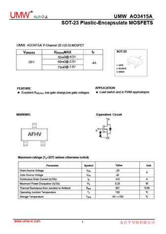
R UMW UMW AO3415A SOT-23 Plastic-Encapsulate MOSFETS UMW AO3415A P-Channel 20-V(D-S) MOSFET SOT-23 ID V(BR)DSS RDS(on)MAX 50m @-4.5V -20V 60m @-2.5V -4A 1. GATE 73m @-1.8V 2. SOURCE 3. DRAIN APPLICATION FEATURE Load switch and in PWM applicatopns Excellent RDS(ON), low gate charge,low gate voltages MARKING Equivalent Circuit D G AFHV S Maximum ratings
0.9. Size:298K msksemi
ao3415ai-ms.pdf
www.msksemi.com AO3415AI-MS Semiconductor Compiance D VDS -20V I (at V =-4.5V) -4A D GS R (at V = -4.5V)
Otros transistores... AO3403, AO3404, AO3404A, AO3406, AO3407A, AO3409, AO3413, AO3414, 75N75, AO3415A, AO3416, AO3418, AO3419, AO3420, AO3421, AO3421E, AO3422