AOTF42S60 MOSFET Equivalente. Reemplazo. Hoja de especificaciones. Principales características
Número de Parte: AOTF42S60
Tipo de FET: MOSFET
Polaridad de transistor: N
ESPECIFICACIONES MÁXIMAS
Pdⓘ - Máxima
disipación de potencia: 50 W
|Vds|ⓘ - Voltaje máximo drenador-fuente: 600 V
|Vgs|ⓘ - Voltaje máximo fuente-puerta: 30 V
|Id|ⓘ - Corriente continua
de drenaje: 39 A
Tjⓘ - Temperatura máxima de unión: 150 °C
CARACTERÍSTICAS ELÉCTRICAS
trⓘ - Tiempo
de subida: 53 nS
Cossⓘ - Capacitancia de salida: 135 pF
RDSonⓘ - Resistencia estado encendido drenaje a fuente: 0.099 Ohm
Encapsulados: TO-220F
Búsqueda de reemplazo de AOTF42S60 MOSFET
- Selecciónⓘ de transistores por parámetros
AOTF42S60 datasheet
..1. Size:271K aosemi
aotf42s60.pdf 

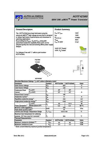
AOTF42S60 TM 600V 39A MOS Power Transistor General Description Product Summary VDS @ Tj,max 700V The AOTF42S60 have been fabricated using the IDM 166A advanced MOSTM high voltage process that is designed to deliver high levels of performance and robustness in RDS(ON),max 0.099 switching applications. Qg,typ 40nC By providing low RDS(on), Qg and EOSS along wit
..2. Size:236K inchange semiconductor
aotf42s60.pdf 

isc N-Channel MOSFET Transistor AOTF42S60 FEATURES Drain Current I = 39A@ T =25 D C Drain Source Voltage- V = 600V(Min) DSS Static Drain-Source On-Resistance R = 99m (Max) DS(on) 100% avalanche tested Minimum Lot-to-Lot variations for robust device performance and reliable operation DESCRITION Be suitable for synchronous rectification for server and gen
0.1. Size:271K aosemi
aotf42s60l.pdf 

AOTF42S60 TM 600V 39A MOS Power Transistor General Description Product Summary VDS @ Tj,max 700V The AOTF42S60 have been fabricated using the IDM 166A advanced MOSTM high voltage process that is designed to deliver high levels of performance and robustness in RDS(ON),max 0.099 switching applications. Qg,typ 40nC By providing low RDS(on), Qg and EOSS along wit
0.2. Size:236K inchange semiconductor
aotf42s60l.pdf 
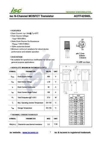
isc N-Channel MOSFET Transistor AOTF42S60L FEATURES Drain Current I = 39A@ T =25 D C Drain Source Voltage- V = 600V(Min) DSS Static Drain-Source On-Resistance R = 99m (Max) DS(on) 100% avalanche tested Minimum Lot-to-Lot variations for robust device performance and reliable operation DESCRITION Be suitable for synchronous rectification for server and ge
9.2. Size:296K aosemi
aotf4s60.pdf 

AOT4S60/AOB4S60/AOTF4S60 TM 600V 4A MOS Power Transistor General Description Product Summary VDS @ Tj,max 700V The AOT4S60 & AOB4S60 & AOTF4S60 have been fabricated using the advanced MOSTM high voltage IDM 16A process that is designed to deliver high levels of RDS(ON),max 0.9 performance and robustness in switching applications. Qg,typ 6nC By providing low RDS
9.3. Size:176K aosemi
aotf474.pdf 

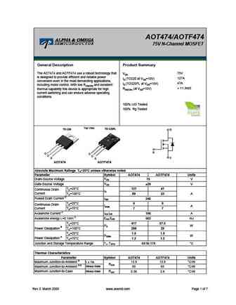
AOT474/AOTF474 75V N-Channel MOSFET General Description Product Summary The AOT474 and AOTF474 use a robust technology that 75V VDS is designed to provide efficient and reliable power 127A ID (TO220 at VGS=10V) conversion even in the most demanding applications, 47A ID (TO220FL at VGS=10V) including motor control. With low RDS(ON) and excellent
9.4. Size:662K aosemi
aotf450a70l.pdf 

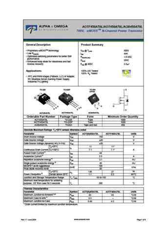
AOTF450A70L/AOT450A70L/AOB450A70L TM 700V, a MOS5 N-Channel Power Transistor General Description Product Summary VDS @ Tj,max 800V Proprietary aMOS5TM technology Low RDS(ON) IDM 44A Optimized switching parameters for better EMI RDS(ON),max
9.6. Size:296K aosemi
aot4s60 aob4s60 aotf4s60.pdf 

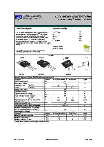
AOT4S60/AOB4S60/AOTF4S60 TM 600V 4A MOS Power Transistor General Description Product Summary VDS @ Tj,max 700V The AOT4S60 & AOB4S60 & AOTF4S60 have been fabricated using the advanced MOSTM high voltage IDM 16A process that is designed to deliver high levels of RDS(ON),max 0.9 performance and robustness in switching applications. Qg,typ 6nC By providing low RDS
9.7. Size:112K aosemi
aotf404.pdf 

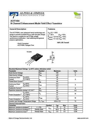
AOTF404 N-Channel Enhancement Mode Field Effect Transistor General Description Features The AOTF404/L uses advanced trench technology and VDS (V) = 105V design to provide excellent RDS(ON) with low gate charge. ID = 26 A (VGS =10V) This device is suitable for use in high voltage RDS(ON)
9.8. Size:185K aosemi
aotf4n90.pdf 

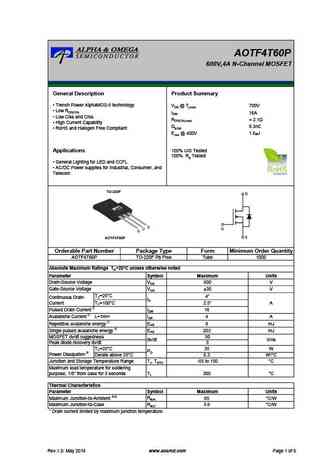
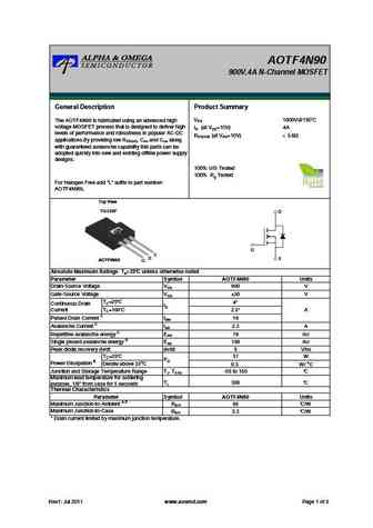
AOTF4N90 900V,4A N-Channel MOSFET General Description Product Summary VDS 1000V@150 The AOTF4N90 is fabricated using an advanced high voltage MOSFET process that is designed to deliver high ID (at VGS=10V) 4A levels of performance and robustness in popular AC-DC RDS(ON) (at VGS=10V)
9.9. Size:441K aosemi
aotf450l.pdf 

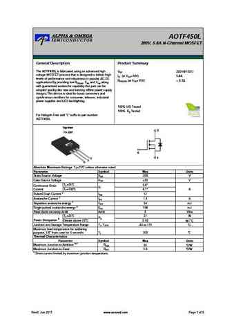
AOTF450L 200V, 5.8A N-Channel MOSFET General Description Product Summary The AOTF450L is fabricated using an advanced high VDS 250V@150 voltage MOSFET process that is designed to deliver high ID (at VGS=10V) 5.8A levels of performance and robustness in popular AC-DC RDS(ON) (at VGS=10V)
9.10. Size:242K aosemi
aotf454l.pdf 

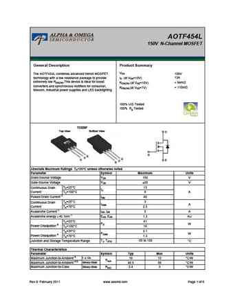
AOTF454L 150V N-Channel MOSFET General Description Product Summary VDS The AOTF454L combines advanced trench MOSFET 150V 13A technology with a low resistance package to provide ID (at VGS=10V) extremely low RDS(ON).This device is ideal for boost
9.11. Size:651K aosemi
aot4n60 aotf4n60 aotf4n60l.pdf 

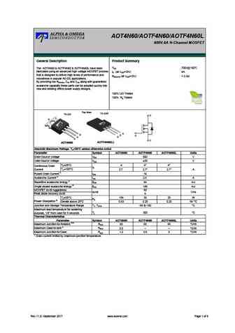
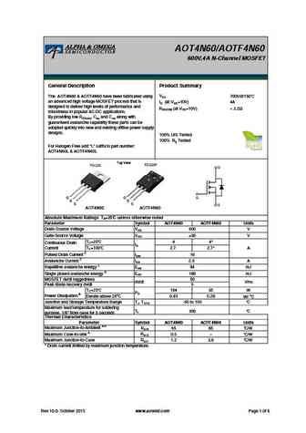
AOT4N60/AOTF4N60/AOTF4N60L 600V,4A N-Channel MOSFET General Description Product Summary VDS 700V@150 The AOT4N60 & AOTF4N60 & AOTF4N60L have been fabricated using an advanced high voltage MOSFET process ID (at VGS=10V) 4A that is designed to deliver high levels of performance and RDS(ON) (at VGS=10V)
9.12. Size:151K aosemi
aotf409.pdf 

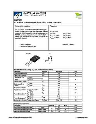
AOTF409 P-Channel Enhancement Mode Field Effect Transistor General Description Features The AOTF409/L uses advanced trench technology to provide excellent RDS(ON), low gate charge and low gate VDS (V) =-60V resistance. With the excellent thermal resistance of the (VGS = -10V) ID = -24A TO220FL package, this device is well suited for high (VGS = -10V) RDS(ON)
9.13. Size:252K aosemi
aotf4n60.pdf 

AOT4N60/AOTF4N60 600V,4A N-Channel MOSFET General Description Product Summary VDS 700V@150 The AOT4N60 & AOTF4N60 have been fabricated using an advanced high voltage MOSFET process that is ID (at VGS=10V) 4A designed to deliver high levels of performance and RDS(ON) (at VGS=10V)
9.14. Size:242K aosemi
aotf4185.pdf 

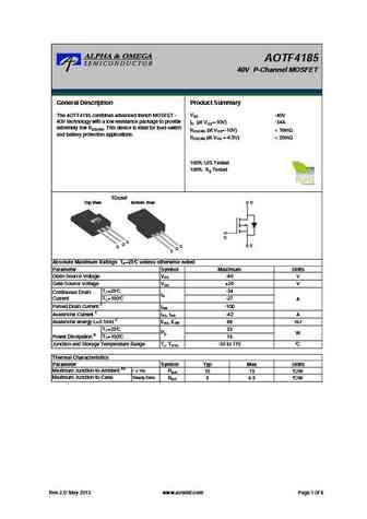
AOTF4185 40V P-Channel MOSFET General Description Product Summary VDS -40V The AOTF4185 combines advanced trench MOSFET - 40V technology with a low resistance package to provide ID (at VGS=-10V) -34A extremely low RDS(ON). This device is ideal for load switch RDS(ON) (at VGS=-10V)
9.15. Size:177K aosemi
aotf472.pdf 

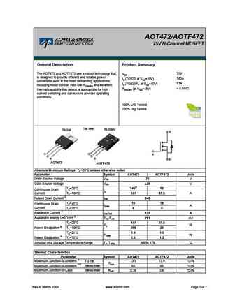
AOT472/AOTF472 75V N-Channel MOSFET General Description Product Summary The AOT472 and AOTF472 use a robust technology that 75V VDS is designed to provide efficient and reliable power 140A ID (TO220 at VGS=10V) conversion even in the most demanding applications, 53A ID (TO220FL at VGS=10V) including motor control. With low RDS(ON) and excellent
9.16. Size:251K inchange semiconductor
aotf4126.pdf 

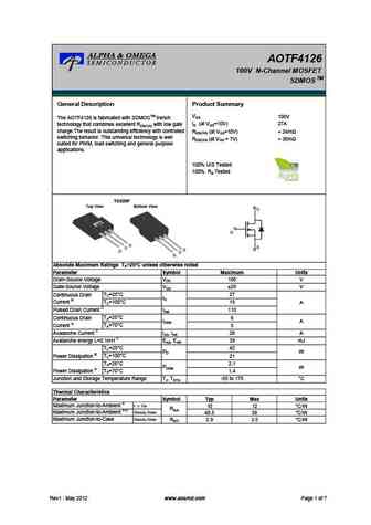
isc N-Channel MOSFET Transistor AOTF4126 FEATURES Drain Current I = 27A@ T =25 D C Drain Source Voltage- V =100V(Min) DSS Static Drain-Source On-Resistance R =24m (Max) DS(on) 100% avalanche tested Minimum Lot-to-Lot variations for robust device performance and reliable operation DESCRIPTION Designed for use in switch mode power supplies and general purpose
9.17. Size:252K inchange semiconductor
aotf4s60.pdf 
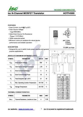
isc N-Channel MOSFET Transistor AOTF4S60 FEATURES Drain Current I =4A@ T =25 D C Drain Source Voltage- V =600V(Min) DSS Static Drain-Source On-Resistance R = 0.9 (Max) DS(on) 100% avalanche tested Minimum Lot-to-Lot variations for robust device performance and reliable operation DESCRIPTION Designed for use in switch mode power supplies and general purpose
9.18. Size:251K inchange semiconductor
aotf474.pdf 

isc N-Channel MOSFET Transistor AOTF474 FEATURES Drain Current I = 47A@ T =25 D C Drain Source Voltage- V =75V(Min) DSS Static Drain-Source On-Resistance R = 11.3m (Max) DS(on) 100% avalanche tested Minimum Lot-to-Lot variations for robust device performance and reliable operation DESCRIPTION Designed for use in switch mode power supplies and general purpos
9.19. Size:252K inchange semiconductor
aotf404.pdf 

isc N-Channel MOSFET Transistor AOTF404 FEATURES Drain Current I = 26A@ T =25 D C Drain Source Voltage- V = 105V(Min) DSS Static Drain-Source On-Resistance R = 28m (Max) DS(on) 100% avalanche tested Minimum Lot-to-Lot variations for robust device performance and reliable operation DESCRIPTION Designed for use in switch mode power supplies and general purpos
9.20. Size:252K inchange semiconductor
aotf4n90.pdf 
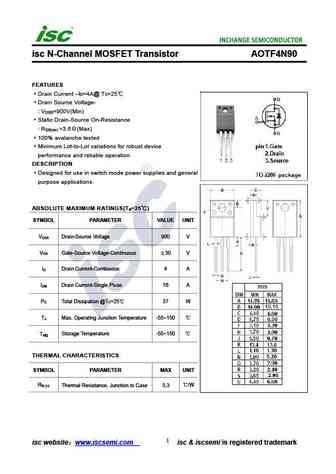
isc N-Channel MOSFET Transistor AOTF4N90 FEATURES Drain Current I =4A@ T =25 D C Drain Source Voltage- V =900V(Min) DSS Static Drain-Source On-Resistance R =3.6 (Max) DS(on) 100% avalanche tested Minimum Lot-to-Lot variations for robust device performance and reliable operation DESCRIPTION Designed for use in switch mode power supplies and general purpose a
9.21. Size:252K inchange semiconductor
aotf450l.pdf 
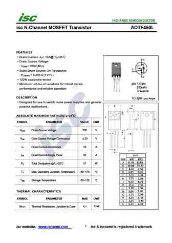
isc N-Channel MOSFET Transistor AOTF450L FEATURES Drain Current I = 10A@ T =25 D C Drain Source Voltage- V = 200V(Min) DSS Static Drain-Source On-Resistance R = 0.265 (TYPE) DS(on) 100% avalanche tested Minimum Lot-to-Lot variations for robust device performance and reliable operation DESCRIPTION Designed for use in switch mode power supplies and general pu
9.22. Size:252K inchange semiconductor
aotf454l.pdf 

isc N-Channel MOSFET Transistor AOTF454L FEATURES Drain Current I = 13A@ T =25 D C Drain Source Voltage- V =150V(Min) DSS Static Drain-Source On-Resistance R =94m (Max) DS(on) 100% avalanche tested Minimum Lot-to-Lot variations for robust device performance and reliable operation DESCRIPTION Designed for use in switch mode power supplies and general purpose
9.23. Size:204K inchange semiconductor
aotf409.pdf 

INCHANGE Semiconductor isc P-Channel MOSFET Transistor AOTF409 FEATURES With TO-220F packaging High speed switching Very high commutation ruggedness Easy to use 100% avalanche tested Minimum Lot-to-Lot variations for robust device performance and reliable operation APPLICATIONS PFC stages LCD & PDP TV Power supply Switching applications ABSOLUTE MAXIMUM
9.24. Size:202K inchange semiconductor
aotf4n60.pdf 
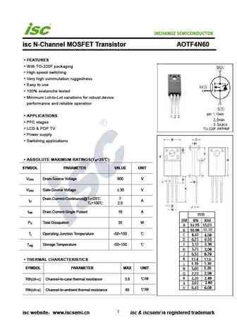
INCHANGE Semiconductor isc N-Channel MOSFET Transistor AOTF4N60 FEATURES With TO-220F packaging High speed switching Very high commutation ruggedness Easy to use 100% avalanche tested Minimum Lot-to-Lot variations for robust device performance and reliable operation APPLICATIONS PFC stages LCD & PDP TV Power supply Switching applications ABSOLUTE MAXIMUM
9.25. Size:252K inchange semiconductor
aotf4185.pdf 
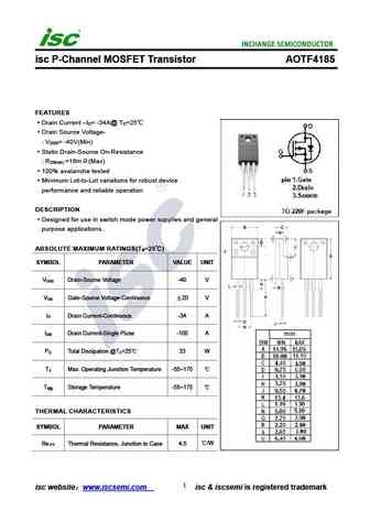
isc P-Channel MOSFET Transistor AOTF4185 FEATURES Drain Current I = -34A@ T =25 D C Drain Source Voltage- V = -40V(Min) DSS Static Drain-Source On-Resistance R =16m (Max) DS(on) 100% avalanche tested Minimum Lot-to-Lot variations for robust device performance and reliable operation DESCRIPTION Designed for use in switch mode power supplies and general purpo
Otros transistores... AOTF3N100
, AOTF3N50
, AOTF3N80
, AOTF3N90
, AOTF404
, AOTF409
, AOTF4126
, AOTF4185
, CS150N03A8
, AOTF42S60L
, AOTF450L
, AOTF454L
, AOTF472
, AOTF474
, AOTF4N60
, AOTF4N90
, AOTF4S60
.
History: MEE4294P-G
| MEE4294K-G
| IAUC90N10S5N062

