APT10050B2VFR MOSFET Equivalente. Reemplazo. Hoja de especificaciones. Principales características
Número de Parte: APT10050B2VFR
Tipo de FET: MOSFET
Polaridad de transistor: N
ESPECIFICACIONES MÁXIMAS
Pdⓘ - Máxima disipación de potencia: 520 W
|Vds|ⓘ - Voltaje máximo drenador-fuente: 1000 V
|Vgs|ⓘ - Voltaje máximo fuente-puerta: 30 V
|Id|ⓘ - Corriente continua de drenaje: 21 A
Tjⓘ - Temperatura máxima de unión: 150 °C
CARACTERÍSTICAS ELÉCTRICAS
trⓘ - Tiempo de subida: 13 nS
Cossⓘ - Capacitancia de salida: 595 pF
RDSonⓘ - Resistencia estado encendido drenaje a fuente: 0.5 Ohm
Encapsulados: TMAX
Búsqueda de reemplazo de APT10050B2VFR MOSFET
- Selecciónⓘ de transistores por parámetros
APT10050B2VFR datasheet
apt10050b2vfr.pdf
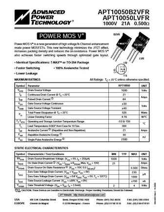
APT10050B2VFR APT10050LVFR 1000V 21A 0.500W B2VR POWER MOS V T-MAX Power MOS V is a new generation of high voltage N-Channel enhancement TO-264 mode power MOSFETs. This new technology minimizes the JFET effect, increases packing density and reduces the on-resistance. Power MOS V also achieves faster switching speeds through optimized gate layout. LVR Identical Specifica
apt10050b2vfrg apt10050lvfrg.pdf
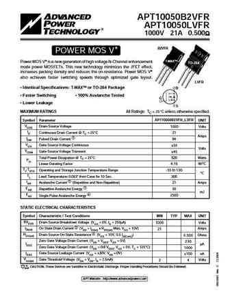
APT10050B2VFR APT10050LVFR 1000V 21A 0.500 B2VFR POWER MOS V T-MAX Power MOS V is a new generation of high voltage N-Channel enhancement TO-264 mode power MOSFETs. This new technology minimizes the JFET effect, increases packing density and reduces the on-resistance. Power MOS V also achieves faster switching speeds through optimized gate layout. LVFR
apt10050b2vr.pdf
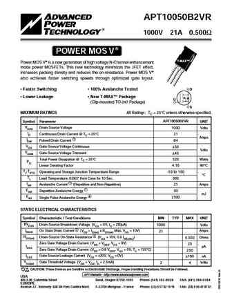
APT10050B2VR 1000V 21A 0.500 POWER MOS V T-MAX Power MOS V is a new generation of high voltage N-Channel enhancement mode power MOSFETs. This new technology minimizes the JFET effect, increases packing density and reduces the on-resistance. Power MOS V also achieves faster switching speeds through optimized gate layout. Faster Switching 100% Avalanche Tested D L
apt10050b2lc.pdf
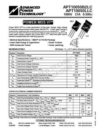
APT10050B2LC APT10050LLC 1000V 21A 0.500W B2LC TM POWER MOS VI T-MAX Power MOS VITM is a new generation of low gate charge, high voltage TO-264 N-Channel enhancement mode power MOSFETs. Lower gate charge is achieved by optimizing the manufacturing process to minimize Ciss and Crss. Lower gate charge coupled with Power MOS VITM optimized gate layout, LLC delivers exceptionally fa

Otros transistores... APT10040B2VFR , APT10040B2VR , APT10045B2FLL , APT10045B2LL , APT10045JFLL , APT10045JLL , APT1004R2KN , APT10050B2LC , MMIS60R580P , APT10050JLC , BUZ50C , APT10078BFLL , APT10078SFLL , APT10078BLL , APT10078SLL , APT10086BLC , APT10086SLC .
History: APT10045JLL | H6N70P
History: APT10045JLL | H6N70P
🌐 : EN ES РУ

Liste
Recientemente añadidas las descripciónes de los transistores:
MOSFET: AUB062N08BG | AUB060N08AG | AUB056N10 | AUB056N08BGL | AUB050N085 | AUB050N055 | AUB045N12 | AUB045N10BT | AUB039N10 | AUB034N10 | AUB033N08BG | AUB026N085 | AUA062N08BG | AUA060N08AG | AUA056N08BGL | AUA039N10
Popular searches
d2390 transistor | 2n5087 equivalent | tip147 datasheet | 2n4124 | mj15022 | toshiba c5198 | irf520n datasheet | tip107