APT5010B2FLL MOSFET Equivalente. Reemplazo. Hoja de especificaciones. Principales características
Número de Parte: APT5010B2FLL
Tipo de FET: MOSFET
Polaridad de transistor: N
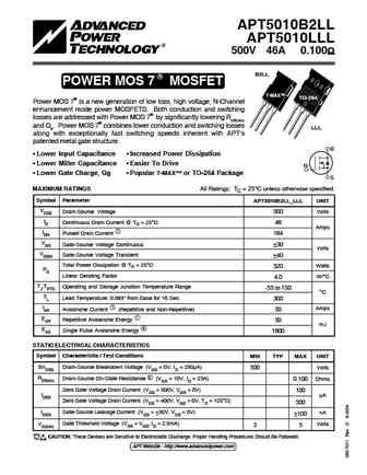
ESPECIFICACIONES MÁXIMAS
Pdⓘ - Máxima disipación de potencia: 500 W
|Vds|ⓘ - Voltaje máximo drenador-fuente: 500 V
|Vgs|ⓘ - Voltaje máximo fuente-puerta: 30 V
|Id|ⓘ - Corriente continua de drenaje: 46 A
Tjⓘ - Temperatura máxima de unión: 150 °C
CARACTERÍSTICAS ELÉCTRICAS
trⓘ - Tiempo de subida: 9 nS
Cossⓘ - Capacitancia de salida: 824 pF
RDSonⓘ - Resistencia estado encendido drenaje a fuente: 0.1 Ohm
Encapsulados: TMAX
Búsqueda de reemplazo de APT5010B2FLL MOSFET
- Selecciónⓘ de transistores por parámetros
APT5010B2FLL datasheet
apt5010b2fll.pdf
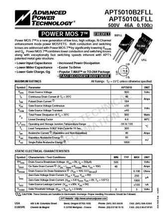
APT5010B2FLL APT5010LFLL 500V 46A 0.100W TM FREDFET POWER MOS 7 B2FLL Power MOS 7TM is a new generation of low loss, high voltage, N-Channel enhancement mode power MOSFETS. Both conduction and switching T-MAX TO-264 losses are addressed with Power MOS 7TM by significantly lowering RDS(ON) and Qg. Power MOS 7TM combines lower conduction and switching losses along with exceptiona
apt5010b2fll.pdf

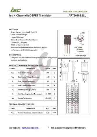
isc N-Channel MOSFET Transistor APT5010B2FLL FEATURES Drain Current I = 46A@ T =25 D C Drain Source Voltage- V =500V(Min) DSS Static Drain-Source On-Resistance R =0.1 (Max) DS(on) 100% avalanche tested Minimum Lot-to-Lot variations for robust device performance and reliable operation DESCRIPTION Designed for use in switch mode power supplies and general pur
apt5010b2fllg apt5010lfllg.pdf
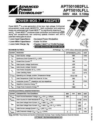
APT5010B2FLL APT5010LFLL 500V 46A 0.100 R B2FLL POWER MOS 7 FREDFET T-MAX Power MOS 7 is a new generation of low loss, high voltage, N-Channel TO-264 enhancement mode power MOSFETS. Both conduction and switching losses are addressed with Power MOS 7 by significantly lowering RDS(ON) and Qg. Power MOS 7 combines lower conduction and switching losses a
apt5010b2vfr.pdf
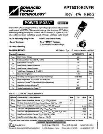
APT5010B2VFR 500V 47A 0.100 POWER MOS V FREDFET T-MAX Power MOS V is a new generation of high voltage N-Channel enhancement mode power MOSFETs. This new technology minimizes the JFET effect, increases packing density and reduces the on-resistance. Power MOS V also achieves faster switching speeds through optimized gate layout. Fast Recovery Body Diode 100% Avalanche


Otros transistores... APT30M36JLL, APT30M40B2VR, APT30M61BLL, APT30M75BLL, APT31N80JC3, APT34N80B2C3, APT4525AN, APT47N60BC3, 10N65, APT5010B2LC, APT5010B2LL, APT5010JFLL, APT5010JLC, APT5010JLL, APT5010JVRU2, APT5010JVRU3, APT5014B2LC
History: 2N7002PW | APT5010B2LC
🌐 : EN ES РУ

Liste
Recientemente añadidas las descripciónes de los transistores:
MOSFET: FTF30P35D | FTF25N35DHVT | FTF15N35D | FTE15C35G | FTP02P15G | FTE02P15G | AKF30N5P0SX | AKF30N10S | AKF20P45D | CM4407 | CM3407 | CM3400 | SVF11N65F | SVF11N65T | FKBB3105 | EHBA036R1
Popular searches
c1213 transistor | 2sc1400 replacement | 2sb817 | mn2488 datasheet | c2026 transistor | 2n3903 transistor | 2n4360 | 2n2613