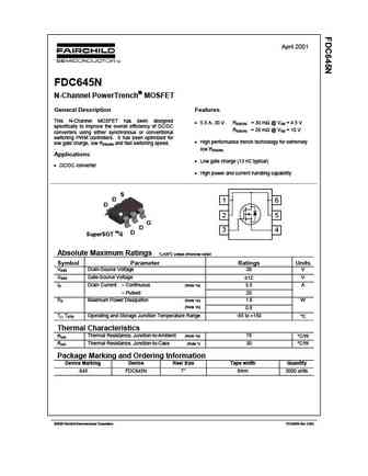
FDC645N MOSFET Equivalente. Reemplazo. Hoja de especificaciones. Principales características
Número de Parte: FDC645N
Tipo de FET: MOSFET
Polaridad de transistor: N
ESPECIFICACIONES MÁXIMAS
Pdⓘ - Máxima
disipación de potencia: 1.6 W
|Vds|ⓘ - Voltaje máximo drenador-fuente: 30 V
|Vgs|ⓘ - Voltaje máximo fuente-puerta: 12 V
|Id|ⓘ - Corriente continua
de drenaje: 5.5 A
Tjⓘ - Temperatura máxima de unión: 150 °C
CARACTERÍSTICAS ELÉCTRICAS
trⓘ - Tiempo
de subida: 9 nS
Cossⓘ - Capacitancia de salida: 227 pF
RDSonⓘ - Resistencia estado encendido drenaje a fuente: 0.03 Ohm
Encapsulados: SSOT6
Búsqueda de reemplazo de FDC645N MOSFET
- Selecciónⓘ de transistores por parámetros
FDC645N datasheet
..3. Size:191K onsemi
fdc645n.pdf 

Is Now Part of To learn more about ON Semiconductor, please visit our website at www.onsemi.com Please note As part of the Fairchild Semiconductor integration, some of the Fairchild orderable part numbers will need to change in order to meet ON Semiconductor s system requirements. Since the ON Semiconductor product management systems do not have the ability to manage part nomenclatur
9.1. Size:241K fairchild semi
fdc642p f085.pdf
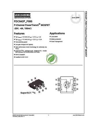
June 2009 FDC642P_F085 P-Channel PowerTrench MOSFET -20V, -4A, 100m Applications Features Load switch Typ rDS(on) = 52.5m at VGS = -4.5V, ID = -4A Battery protection Typ rDS(on) = 75.3m at VGS = -2.5V, ID = -3.2A Power management Fast switching speed Low gate charge(6.9nC typical) High performance trench technology for extremely low rDS(on) SuperSOTTM-6
9.2. Size:76K fairchild semi
fdc6401n.pdf
October 2001 FDC6401N Dual N-Channel 2.5V Specified PowerTrench MOSFET General Description Features This Dual N-Channel MOSFET has been designed 3.0 A, 20 V. RDS(ON) = 70 m @ VGS = 4.5 V specifically to improve the overall efficiency of DC/DC RDS(ON) = 95 m @ VGS = 2.5 V converters using either synchronous or conventional switching PWM controllers. It has been optimiz
9.3. Size:76K fairchild semi
fdc640p f095.pdf
January 2001 FDC640P P-Channel 2.5V PowerTrench Specified MOSFET General Description Features This P-Channel 2.5V specified MOSFET uses a rugged 4.5 A, 20 V RDS(ON) = 0.053 @ VGS = 4.5 V gate version of Fairchild s advanced PowerTrench RDS(ON) = 0.080 @ VGS = 2.5 V process. It has been optimized for power management applications with a wide r
9.5. Size:78K fairchild semi
fdc640p.pdf

January 2001 FDC640P P-Channel 2.5V PowerTrench Specified MOSFET General Description Features This P-Channel 2.5V specified MOSFET uses a rugged 4.5 A, 20 V RDS(ON) = 0.053 @ VGS = 4.5 V gate version of Fairchild s advanced PowerTrench RDS(ON) = 0.080 @ VGS = 2.5 V process. It has been optimized for power management applications with a wide r
9.6. Size:266K fairchild semi
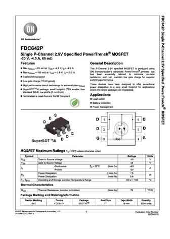
fdc642p.pdf
January 2010 FDC642P Single P-Channel 2.5V Specified PowerTrench MOSFET -20 V, -4.0 A, 65 m Features General Description Max rDS(on) = 65 m at VGS = -4.5 V, ID = -4.0 A This P-Channel 2.5V specified MOSFET is produced using Fairchild s advanced PowerTrench process that has been Max rDS(on) = 100 m at VGS = -2.5 V, ID = -3.2 A especially tailored to minimize on-state
9.7. Size:1310K onsemi
fdc642p-f085 fdc642p-f085p.pdf
MOSFET P-Channel, POWERTRENCH -20 V, -4 A, 100 mW FDC642P-F085, FDC642P-F085P www.onsemi.com Features Typ RDS(on) = 52.5 mW at VGS = -4.5 V, ID = -4 A Typ RDS(on) = 75.3 mW at VGS = -2.5 V, ID = -3.2 A Fast Switching Speed Low Gate Charge (6.9 nC Typical) TSOT23 6-Lead High Performance Trench Technology for Extremely Low RDS(on) CASE 419BL SUPERSOTt-6 P
9.8. Size:190K onsemi
fdc6401n.pdf

Is Now Part of To learn more about ON Semiconductor, please visit our website at www.onsemi.com Please note As part of the Fairchild Semiconductor integration, some of the Fairchild orderable part numbers will need to change in order to meet ON Semiconductor s system requirements. Since the ON Semiconductor product management systems do not have the ability to manage part nomenclatur
9.10. Size:1570K kexin
fdc642p.pdf
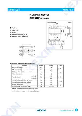
SMD Type MOSFET P-Channel MOSFET FDC642P (KDC642P) ( ) SOT-23-6 Unit mm +0.1 0.4 -0.1 6 5 4 Features VDS (V) =-20V ID =-4 A RDS(ON) 65m (VGS =-4.5V) 2 3 1 +0.02 RDS(ON) 100m (VGS =-2.5V) 0.15 -0.02 +0.01 -0.01 +0.2 -0.1 D D 6 1 D D 5 2 G S 4 3 Absolute Maximum Ratings Ta = 25 Parameter Symbol Rating Unit Drain-Source Vol
9.11. Size:1544K cn vbsemi
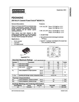
fdc6420c.pdf
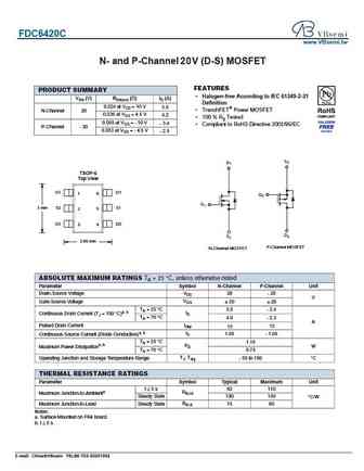
FDC6420C www.VBsemi.tw N- and P-Channel 2 V (D-S) MOSFET 0 FEATURES PRODUCT SUMMARY Halogen-free According to IEC 61249-2-21 VDS (V) RDS(on) ( )ID (A) Definition 0.024 at VGS = 10 V 5.5 TrenchFET Power MOSFET N-Channel 20 0.036 at VGS = 4.5 V 4.2 100 % Rg Tested 0.069 at VGS = - 10 V - 3.4 Compliant to RoHS Directive 2002/95/EC P-Channel - 20 0.083 at V
Otros transistores... FQB46N15
, FQI46N15
, FQP10N50CF
, FDB86366F085
, FCH077N65FF085
, FCH190N65FF085
, FQT2P25
, FQU1N80
, 20N60
, SI3457DV
, SSU1N50B
, FDP070AN06A0
, FQPF5N60C
, FQP9N50C
, FQPF9N50C
, FDD6296
, FCP16N60
.